
Negative differential transconductance device with a stepped gate dielectric for multi-valued logic circuits†
Maksim
Andreev‡
a,
Jae-Woong
Choi‡
b,
Jiwan
Koo
a,
Hyeongjun
Kim
a,
Sooyoung
Jung
a,
Kwan-Ho
Kim
a and
Jin-Hong
Park
 *ab
*ab
aDepartment of Electrical and Computer Engineering, Sungkyunkwan University, Suwon 16419, Korea. E-mail: jhpark9@skku.edu
bSKKU Advanced Institute of Nano Technology (SAINT), Sungkyunkwan University, Suwon 16419, Korea
First published on 29th July 2020
Abstract
Multi-valued logic (MVL) technology is a promising approach for improving the data-handling capabilities and decreasing the power consumption of integrated circuits. This is especially attractive as conventional complementary metal–oxide–semiconductor technology is approaching its scaling and power density limits. Here, an ambipolar WSe2 field-effect transistor with two or more negative-differential-transconductance (NDT) regions in its transfer characteristic (NDTFET) is proposed for MVL applications of various radices. The operation and charge carrier transport mechanism of the NDTFET are studied first by Kelvin probe force microscopy, electrical, and capacitance–voltage measurements. Next, strategies for increasing the number of NDT regions and engineering the NDTFET transfer characteristic are discussed. Finally, the extensibility and tunability of our concept are demonstrated by adapting NDTFETs as core devices for ternary, quaternary, and quinary MVL inverters through simulations, where only WSe2 is employed as a channel material for all devices comprising the inverters. The MVL inverter operation principle and the mechanism of the multiple logic state formation are analyzed in detail. The proposed concept is practically verified by the fabrication of a ternary inverter.
New conceptsComplementary metal–oxide–semiconductor (CMOS) technology suffers from power density limits and increasing signal propagation delay, which are dominated by interconnects. These issues can be overcome with the multi-valued logic (MVL) approach, where conventional binary systems are replaced by systems with higher radices. This work proposes an MVL unit device – a novel concept of single-material WSe2 field-effect transistors with a tunable number of threshold voltages (VTH) – to overcome the bit-density limitation of conventional binary systems. Our devices featuring a stepped gate dielectric – although structurally resembling conventional devices for binary systems – effectively combine the functionality of several devices in a single device without additional interconnects. Previously reported unit devices for MVL systems had complex heterojunction channels, which complicated fabrication and introduced an additional interface that could affect the electrical performance. Besides, they were conceptually limited to a specific number of VTH, which in turn limited their applicability to systems of only a specific radix (3 or maximum 4). Our concept enables the first demonstration of a quinary (5-state) inverter along with designing other basic MVL building blocks such as 3-state and 4-state inverters within the same concept. Moreover, we reveal that basic MVL circuits can be designed using only devices with WSe2 as a channel material. |
Introduction
Complementary metal–oxide–semiconductor (CMOS) technology has evolved over many years by downscaling the device dimensions.1 However, the increase in device density has been accompanied by growing power consumption due to parasitic capacitances and resistances of interconnect lines, whose overall length and complexity have grown with each new technological node.2 The multi-valued logic (MVL) concept has been considered as a solution to resolve the interconnect problem, because a system with similar performance can be implemented with fewer devices and interconnects owing to higher functionality of MVL circuits.3 For example, the transition from a binary system to a ternary, quaternary, or quinary system is estimated to decrease the system complexity to 63.1%, 50%, or 43.1%, respectively.4 Although various binary CMOS-based MVL circuits have been demonstrated, which could serve as a proof-of-concept for MVL systems, their realization required a large number of CMOS devices, which negated the key advantages of the MVL concept.5,6 Therefore, conceptually new devices suitable for MVL systems are required, just as the CMOS transistor is suitable for binary very large scale integration systems.A common strategy to realize a device suitable for MVL circuits is to introduce an additional threshold voltage(s) (Vth) into the current–voltage (I–V) characteristics by using the negative differential resistance (NDR) phenomenon – realized, for instance, in Esaki diodes,7–11,27 resonant tunneling diodes,12–15 Gunn diodes,16 single-electron transistors,17,18 and molecular devices19,20 – or by the negative differential transconductance (NDT) phenomenon.21–38 The NDR- and NDT-devices are designed to have I–V characteristics with region(s) where the drain current (ID) decreases when the drain-to-source voltage (for NDR) or the gate voltage (for NDT) continues to increase, consequently forming multiple Vth. When two or more Vth are present, the I–V characteristics of an MVL device and load device can be matched to provide multiple logic states. Because devices with multiple Vth often require various types of heterojunctions with high interfacial quality, van der Waals (vdW) layered materials (such as MoS2, WSe2, h-BN, etc.) with very low surface defect densities have been employed for the implementation of MVL devices and circuits in recent years.21–29 Besides, individual layers of vdW materials are coupled by weak vdW forces, thereby allowing atomically sharp junctions with high-quality interfaces by simple mechanical stacking despite a significant lattice mismatch.39
Although NDR devices with more than one Vth have been realized, implementation of a basic building block – a ternary inverter – requires at least three Vth in the case of NDR-devices, whereas only two Vth are sufficient in the case of NDT-devices.21 Moreover, in contrast to three-terminal NDT-based devices, two-terminal NDR-devices with folded I–V characteristics have inherent hysteresis when loaded with other devices for logic applications – an undesirable effect which requires additional circuitry solutions.40,41 Recently, the NDT phenomenon has also been extensively researched, and ternary and quaternary inverters which make use of NDT have been demonstrated.21–34 However, their realization commonly required heterojunction-based channels consisting of at least two materials. Besides, NDT-device concepts that can be easily extended to logic circuits of higher radices are still lacking.
Here, we report a WSe2-based NDT field-effect transistor (NDTFET) with two or more NDT regions in its transfer characteristic for MVL applications of various radices. These multiple NDT regions are induced by creating two or more electrically different regions along the transistor channel via gate dielectric engineering. We first provide detailed analysis of the operational principle and charge carrier transport mechanism using Kelvin Probe Force Microscopy (KPFM) and capacitance–voltage and electrical characteristics. Next, methods for engineering a transfer characteristic of a desired shape are proposed and studied. Finally, we show the extensibility and feasibility of the proposed concept by applying it to ternary, quaternary, and quinary MVL inverter circuits with simulations together with practical implementation of a ternary inverter.
Results and discussion
The schematic and circuit symbols of the NDTFET are shown in Fig. 1a. The WSe2 channel was mechanically transferred onto the h-BN gate dielectric with two regions having different thicknesses (th-BN and Th-BN, where th-BN and Th-BN denote the thicknesses of the parts with thinner and thicker gate dielectrics, respectively). The gate bias (VG) is applied through the back Au gate. The Ti/Au contacts deposited on the WSe2 channel serve as source and drain electrodes. The Fermi level of the low-work-function Ti contacts tends to pin near the mid-gap of WSe2,42 which enables either electron or hole injection depending on the applied VG (Fig. S1, ESI†). The ambipolarity of the channel is a crucial requirement for the induction of the NDT phenomenon, as it will be seen later. The use of the bottom-gate structure is dictated by research purposes, particularly to be able to access the top surface of the channel and evaluate the performance of each part (th-BN and Th-BN) separately by forming additional metal contacts. In this structure, the channel is inevitably bent and a small air gap is formed beneath the bent part. We confirmed its negligible effect on the NDTFET performance, which will be discussed in the following paragraphs. Here, h-BN was chosen as a gate dielectric owing to its layered structure, which favors the formation of a superior interface with layered WSe2 and minimizes the hysteresis in the transfer characteristic of the WSe2 transistor (Fig. S2, ESI†). The cross-sectional transmission electron microscopy (X-TEM) image (Fig. 1b, top image) and top-view optical image of the whole device (Fig. 1b, bottom image) show the structure of the NDTFET fabricated in the course of this study. Here, dimensional parameters such as th-BN, Th-BN, the channel length, and the channel width are selected from a wide range of values depending on the experimental purpose. In higher-magnification X-TEM images of the h-BN/h-BN and h-BN/WSe2 interfaces (Fig. 1c, top image) there are no visible polymer residues owing to our transfer technique, which utilizes the difference between the adhesion energies at different interfaces (Fig. S3, ESI†). The elemental analysis of the interfaces through high-resolution electron energy loss spectroscopy (Fig. 1c, bottom image) shows the abrupt atomic distribution.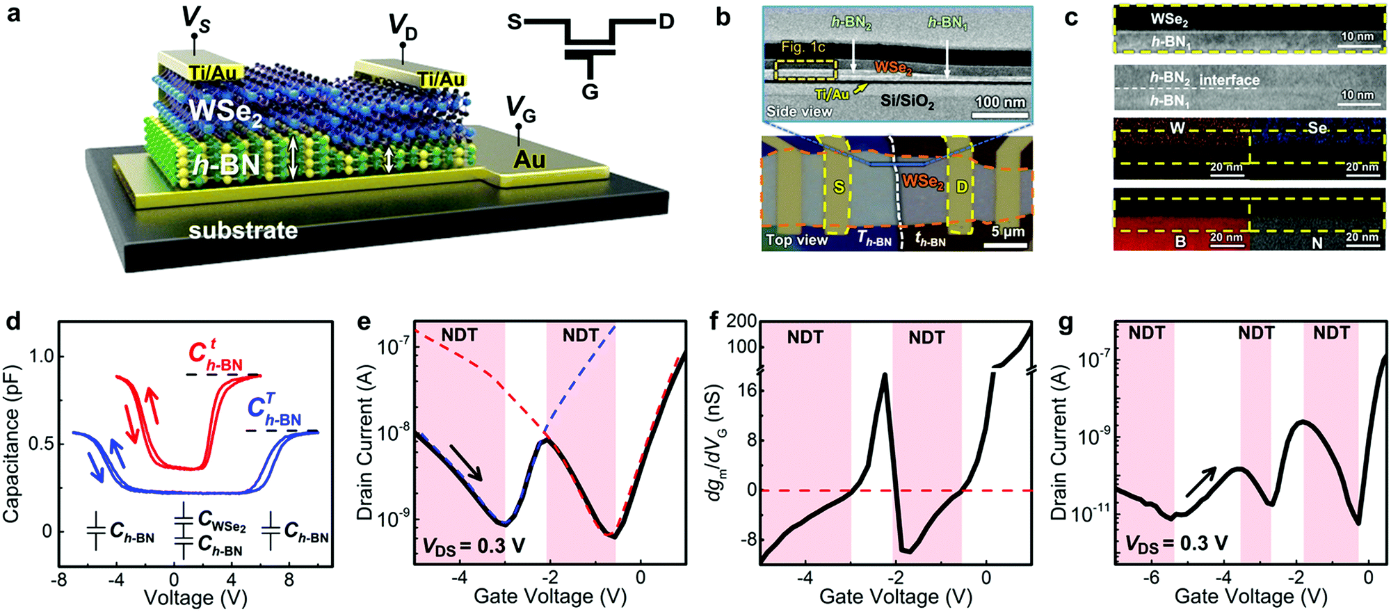 | ||
| Fig. 1 Structure and properties of the NDTFET. (a) Schematic and circuit symbols of the NDTFET. (b) Cross-sectional transmission electron microscopy image (top) and top-view optical image (bottom) of the NDTFET. (c) Higher-magnification X-TEM image of the h-BN/WSe2 and h-BN/h-BN interfaces (top) and high-resolution electron energy loss spectroscopy image of the h-BN/WSe2 interface (bottom). (d) Capacitance–voltage characteristics of the Au/h-BN/WSe2 structures for th-BN = 76 nm (red curve) and Th-BN = 230 nm (blue curve); the arrows indicate the sweep directions of the gate voltage. (e) Transfer characteristic of the NDTFET (black solid line) with highlighted NDT regions, and transfer characteristics of parts with th-BN (red dashed line) and Th-BN (blue dashed line); the arrow indicates the sweep direction of the gate voltage. (f) The differential transconductance (dgm/dVG) as a function of the gate voltage. The red dashed line indicates the zero level of dgm/dVG. (g) Two-peak transfer characteristic of the NDTFET. | ||
The high-quality of the WSe2/h-BN and h-BN/h-BN interfaces leads to minimized hysteresis in the capacitance–voltage (C–V) characteristics of the metal/insulator/semiconductor (MIS) structures consisting of Au, h-BN, and WSe2 (Fig. 1d). Particularly, although a larger thickness of the gate dielectric (Th-BN) is obtained by stacking two h-BN flakes, the hysteresis remains small. The overall capacitance of the MIS structure (CMIS) can be regarded as the capacitance of the h-BN gate dielectric (Ch-BN) in series with the capacitance of the WSe2 channel (CWSe2). Let us first consider the red C–V characteristic of the part with thinner h-BN (th-BN). For a negative VG < −2 V, the Fermi level of WSe2 is near the valence band (VB), where the injection of holes from the Ti contact is favorable. The channel accumulates holes (see Fig. S1 in the ESI†) and only a contribution from Ch-BN is observed. When VG is increased, the Fermi level of the channel approaches the mid-gap, where the hole and electron injection are hindered by high Schottky barriers. In this regime between VG = −2 and 2 V, which is referred to here and further as a quasi-insulating regime, the capacitance CWSe2 is added in series with Ch-BN, which decreases CMIS to its lowest value. Similar to the case of hole accumulation, when VG > 2 V, electrons are injected into the conduction band (CB), which leads to their accumulation and a corresponding increase in CMIS back to Ch-BN. The blue C–V characteristic corresponds to the MIS capacitor with thicker h-BN (Th-BN). Owing to the larger thickness of h-BN, the capacitance of Ch-BN (electron and hole accumulation regimes) and the capacitance of CWSe2 in series with Ch-BN (the quasi-insulating regime) are lower. With thicker h-BN, the induced electric field is weaker; therefore, more negative VG is required to deplete the channel of electrons injected from the source. This leads to a negative shift of the minimum-CMIS region, or, in other words, to different Vth for the electron and hole accumulation regimes in the part with Th-BN. The demonstrated difference in electrical properties between the two regions results in unusual device operation (Fig. 1e); the transfer characteristic of the NDTFET exhibits two drain current (ID) minima at VG = −3 V and −0.8 V, and two NDT regions (between −5 and −3 V and between −2.1 and −0.7 V) where ID decreases when VG is swept from negative to positive values. Further, we focus on the NDT in the range from −2.1 to −0.7 V, which is an abnormal characteristic of this device, whereas the NDT region from −5 to −3 V is a normal p-channel operation region of an ambipolar transfer characteristic. Here and throughout the manuscript, we intentionally show only low-current regions of the NDTFET transfer characteristics in the vicinity of current peaks and current minima, which is the operational range of our devices and circuits. Unlike a conventional binary MOSFET, our MVL NDTFETs do not operate in the fully on-state, and thereby the on-state parts of the transfer characteristics are not considered further. The blue and red dashed lines indicate transfer characteristics measured on the parts with Th-BN and th-BN, respectively, after deposition of additional Ti/Au contacts along the NDTFET channel. They show contributions to the transfer characteristic of the NDTFET from each region. The dependence of the differential transconductance (dgm/dVG) on VG, derived from the transfer characteristic in Fig. 1e, shows two NDT regions highlighted with red color (Fig. 1f). We also implemented a two-peak transfer characteristic (Fig. 1g) by expanding the NDTFET concept and fabricating an NDTFET with three regions of different h-BN thicknesses. Its transfer characteristic correspondingly has three ID minima and three NDT regions.
Kelvin probe force microscopy (KPFM) analysis is then carried out to investigate the abnormal electrical behavior through the distribution of the contact potential difference (VCPD) between the tip and surface of the NDTFET under different VG values (Fig. 2a; for details see the Experimental section). The results show an uneven surface potential distribution and the presence of a built-in electric field between the two regions (Th-BN and th-BN) strongly dependent on VG (Fig. 2b). We note that the surface potential of the bent part of the channel also shows a strong dependence on VG and follows the variations along with the rest of the channel, inferring efficient gating of the bent part and its negligible effect on the NDTFET performance. A difference in VCPD up to approximately 300 mV is observed between the two channel regions, which is minimized at VG = −7 or −2 V. The KPFM maps of VCPD over the channel surface for the two representative VG values of −2 V (VCPD is maximized) and −7 V (VCPD is minimized) are shown in Fig. 2c.
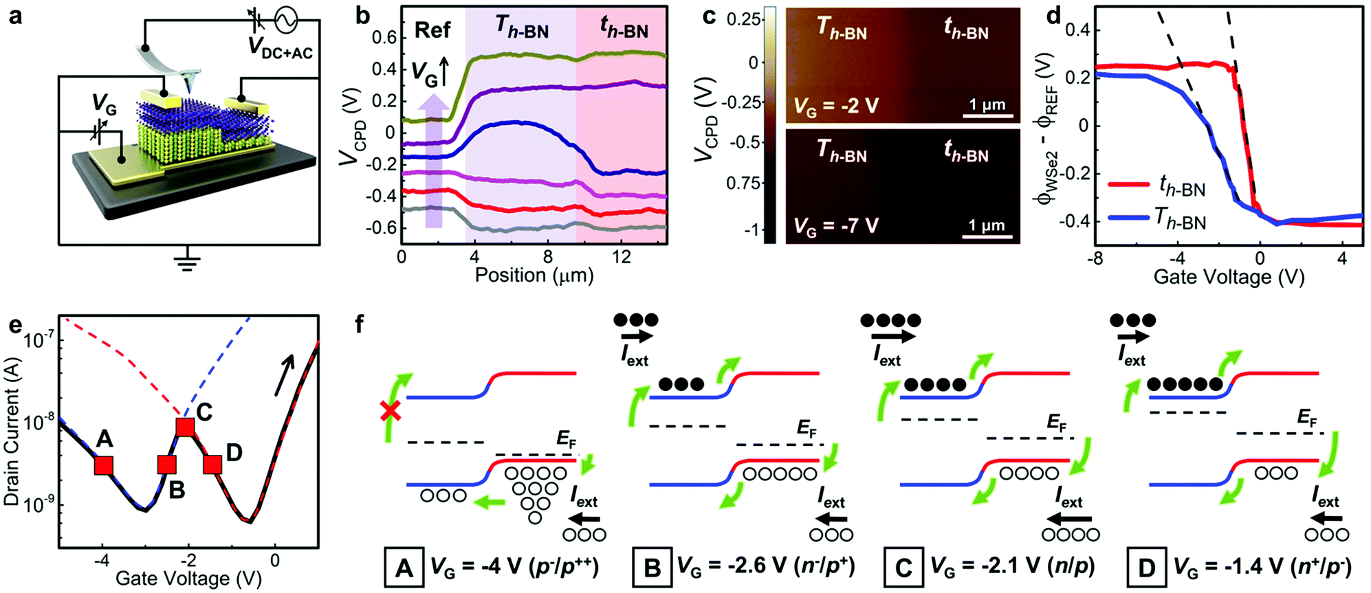 | ||
| Fig. 2 Operational principle and charge carrier transport of the NDTFET. (a) Schematic of the Kelvin probe force microscopy measurement. (b) Contact potential difference (VCPD) profiles along the NDTFET at different gate voltages (VG); the reference value of VCPD is recorded on the surface of Au. (c) Contact potential difference (VCPD) maps for gate voltages VG = −2 and −7 V, when the difference in VCPD between the regions with th-BN and Th-BN is maximized and minimized, respectively. (d) Difference between the work function of WSe2 and the reference work function of Au (ΦWSe2 − ΦRef) as a function of VG for the parts with th-BN (red curve) and Th-BN (blue curve); the black dashed lines indicate the slopes of the demonstrated dependences. (e) Typical transfer characteristic of the NDTFET (black solid line), and transfer characteristics of parts with th-BN (red dashed line) and Th-BN (blue dashed line). The arrow indicates the sweep direction of the gate voltage. The labeled red squares denote four characteristic gate biases VG = −4, −2.6, −2.1, and −1.4 V corresponding to different operational regimes of the NDTFET. (f) Representation of the charge carrier transport in the NDTFET at four characteristic gate biases VG = −4, −2.6, −2.1, and −1.4 V demonstrated with band diagrams. | ||
The difference between the work function of WSe2 (ΦWSe2) and the reference work function (ΦRef) is plotted against VG (Fig. 2d) for both parts (Th-BN and th-BN). A comparison of the slopes related to these dependences shows more rapid change of (ΦWSe2 − ΦRef) in the region with th-BN, which is consequently indicative of more efficient gate control over the channel compared to the region with Th-BN. In other words, more negative VG is needed for the region with Th-BN to reach the quasi-insulating regime. Based on the results obtained from the KPFM measurements and the previously measured current/capacitance–voltage characteristics, we infer the charge transport mechanism and suggest the following operational principle. At VG = −4 V (point A in Fig. 2e), both regions th-BN and Th-BN accumulate holes, which can be seen from the transfer characteristics of each part. However, because VG = −4 V is near the quasi-insulating regime for the region Th-BN, a comparatively smaller hole carrier concentration is expected. We denote this state as a unipolar p−/p++ junction where the hole current is limited by the potential barrier between the two regions (band diagram A in Fig. 2f). When VG exceeds −2.5 V (point B), the region Th-BN starts to accumulate electrons (its electron concentration is denoted as n−), whereas the region with th-BN still operates in the hole accumulation regime (marked as p+). Thus, the device essentially behaves as an asymmetric n−/p+ junction where the regions with Th-BN and th-BN act as n- and p-type semiconductors, respectively (band diagram B in Fig. 2f). Majority carriers from the n- and p-sides are swept across the junction under the forward bias and become minority carriers, followed by their recombination. The recombined electron–hole pairs are resupplied from the external circuit (Iext), but electrons available for recombination (n−) in the CB are fewer than holes in the VB (p+). Therefore, the number of resupplied electron–hole pairs is limited by n−. In other words, the injection of electrons from the source is a limiting factor for the current flow at point B and thus ID closely follows the branch corresponding to the electron conductivity of region Th-BN (blue dashed curve). With a further increase in VG, more electrons (marked as n) and fewer holes (p) are accumulated in regions with Th-BN and th-BN, respectively. As the electron concentration continues to increase, which thus increases ID, it remains the limiting factor until the concentrations of majority carriers in parts with Th-BN and th-BN become almost equal (VG ≈ −2.1 V, point C, band diagram C in Fig. 2f). If VG is further increased (point D), behavior opposite to that in point B is manifested, i.e., more electrons (n+) and fewer holes (p−) are accumulated in parts with Th-BN and th-BN, respectively (band diagram D in Fig. 2f). The injection of holes from the drain becomes a limiting factor, and thus ID follows the hole branch of the transfer characteristic of the part with th-BN, where ID decreases (red dashed curve). With the decrease in ID, a local ID maximum and an NDT region are formed. When VG exceeds −0.7 V, both regions are in electron accumulation regimes and behavior analogous to that in point A is observed.
Because NDT regions are crucial for generating additional logic states in NDT-based MVL circuits, control over parameters of the NDT transfer characteristic, such as the peak voltage (VPEAK), minimum voltages (Vm), and peak-to-valley current ratio (PVCR), is desirable. If the thicknesses th-BN and Th-BN are properly selected, an NDTFET with predictable Vm values can be designed. A device having three regions of different gate dielectric thickness (68 nm, 83 nm, and 134 nm) is fabricated to demonstrate the effect of the gate dielectric thickness on the transfer characteristics (Fig. 3a). The shift of Vm to more negative VG values is observed with increasing the gate dielectric thickness (Fig. 3b and c); the thickness of the h-BN flakes was measured by using atomic force microscopy (see the Experimental section). For illustration, two NDTFETs with different NDT curves (blue curve th-BN = 157 nm, Th-BN = 225 nm; red: th-BN = 83 nm, Th-BN = 134 nm) are designed and fabricated (Fig. 3d). The VPEAK values of these curves are shifted from each other by 2 V. The channel length (LCH) is another parameter that can be used for tuning and modeling the NDT characteristic curve. We note that NDTFET transfer characteristics are reproducible and remain stable under multiple cycles of measurements (Fig. S4, ESI†). For an NDTFET with two regions of different gate dielectric thicknesses, LCH can be represented as a sum of the channel lengths of the regions with thinner (Lt) and thicker (LT) gate dielectrics, LCH = Lt + LT. We formed additional electrodes to examine effect of LT on the NDTFET transfer characteristic, where LT was varied from 9 to 21 μm (Fig. 3e). As previously explained in Fig. 2f, ID of the NDTFET is limited by different channel parts (Th-BN or th-BN) depending on the applied VG. The value of VG that separates these modes is the peak voltage (VPEAK). For example, VPEAK is approximately −1.9 V for the NDTFET transfer characteristic obtained for LT = 9 μm (Fig. 3f). This implies that ID is limited by the region with th-BN for VG > −1.9 V, whereas the region with Th-BN defines ID for VG < −1.9 V. Accordingly, a variation in LT is expected to have only a small impact on ID for VG > −1.9, but a large impact on ID for VG < −1.9 V, whereas the opposite behavior is anticipated for the variation in Lt. This enables independent tuning of the NDTFET transfer characteristic for VG > VPEAK or VG < VPEAK by varying Lt or LT, respectively. We experimentally show the feasibility of the tuning by varying LT. When LT decreases, only ID for VG < −1.9 V is mostly increased. Consequently, this is accompanied by the shift of VPEAK to more negative VG values (Fig. 3g), an increase in IPEAK (Fig. 3g), and an increase in PVCR (Fig. 3h). As the current is weakly influenced by LT when VG > VPEAK, IVALLEY and VVALLEY (right-side valley) remain almost constant (Fig. S5, ESI†).
 | ||
| Fig. 3 Tunability of the NDTFET. (a) Schematic and top-view optical image of the device having three regions of different gate dielectric thickness (68 nm – Region 1, 83 nm – Region 2, and 134 nm – Region 3) with additional pairs of source and drain electrodes fabricated to analyze the tunability of the minimum voltages (Vm) with the gate dielectric thickness. (b) Transfer characteristics of each of the three regions shown in (a). The blue, red, and green curves correspond to Region 1, 2, and 3 shown in (a). (c) Vm as a function of the gate dielectric thickness. (d) Transfer characteristics of single-peak NDTFETs obtained by choosing different sets of th-BN and Th-BN (blue curve: th-BN = 157 nm, Th-BN = 225 nm; red curve: th-BN = 83 nm, Th-BN = 134 nm). (e) Schematic and top-view optical image of the NDTFET (th-BN = 65 nm, Th-BN = 198 nm) with additional source electrodes on the part with Th-BN fabricated to analyze the tunability of the NDTFET transfer characteristic with the channel length of the part with Th-BN (LT). Lt = 6 μm, LT1 = 9 μm, LT2 = 14 μm, LT3 = 21 μm. (f) Transfer characteristics of the NDTFET as a function of LT. (g) Peak voltage (VPEAK) and peak current (IPEAK) of the NDTFET transfer characteristic as function of LT extracted from (f). (h) Peak-to-valley current ratio (PVCR) as a function of LT extracted from (f). | ||
Finally, we show the application of the proposed concept for the realization of basic MVL gates such as MVL inverters through simulations and experiments. We present a detailed analysis of quinary (5 logic states) MVL inverter operation through simulations (Fig. 4 and Fig. S6, Video S1, ESI†); data related to a simulated quaternary MVL inverter (4 logic states) along with simulated and experimentally verified ternary (3 logic states) MVL inverters realized with similar principles are available in Fig. S7–S9 in the ESI.† The table-lookup-based models of the NDTFET and load devices based on experimental data are developed in the Verilog-A language and then used for the inverter simulation in the Cadence® Spectre® simulation platform. The quinary inverter consists of models of an NDTFET having four regions of different gate dielectric thicknesses (82 nm, 150 nm, 212 nm, and 238 nm) whose transfer characteristic has four ID minima and four NDT regions; the load device is represented by a WSe2 ambipolar TFT with Ti/Au contacts (Fig. 4a). Thus, all models comprising the inverter are based on experimental data obtained from devices with only WSe2 as a channel material. To produce additional logic states in this configuration, Vm of the load WSe2 device is selected to have more negative Vm than the most negative Vm among the four Vm values of the three-peak NDTFET, which is realized by using a thicker gate dielectric. The input voltage (VIN) is applied simultaneously to the gate terminals of the NDTFET and load. The output voltage (VOUT) is read across the load device. When VIN is swept from −5.25 to −1.3 V and VDD = 1.5 V, five regions of almost constant VOUT values are observed, which can function as stable logic states (Fig. 4b). Thus, we can define logic states “4” (VOUT ≈ 1.4 ± 0.02 V) for −5.25 V < VIN < −4.75 V; “3” (VOUT ≈ 0.96 ± 0.01 V) for −4.4 V < VIN < −3.9 V; “2” (VOUT ≈ 0.59 ± 0.02 V) for −3.5 V < VIN < −3 V; “1” (VOUT ≈ 0.31 ± 0.01 V) for −2.65 V < VIN < −2.2 V; and “0” (VOUT ≈ 0.02 ± 0.01 V) for −1.8 V < VIN < −1.3 V.
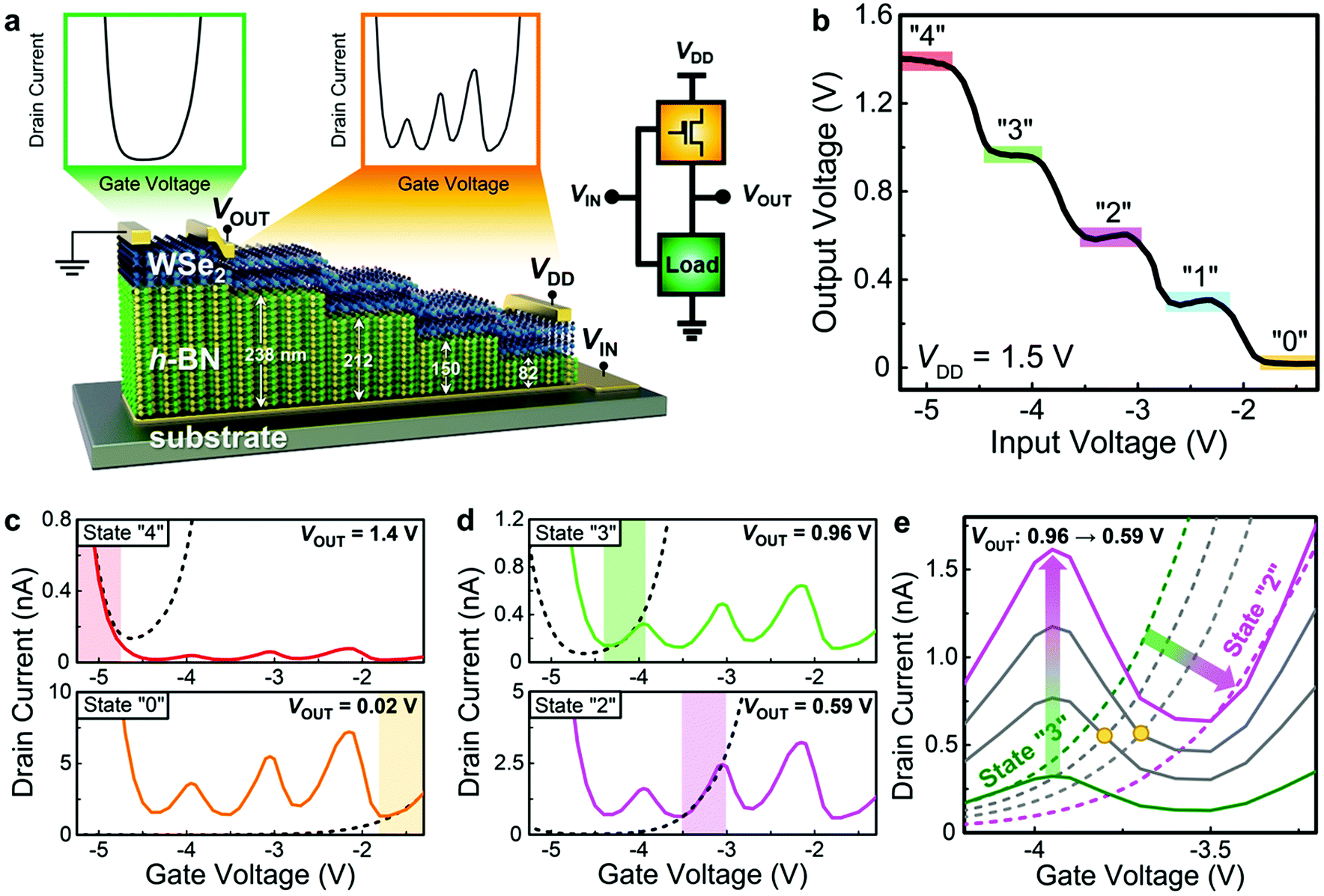 | ||
| Fig. 4 Quinary inverter. (a) Schematic representation and circuit diagram of the quinary inverter. (b) Input–output characteristic of the quinary inverter. (c and d) Transfer characteristics of the NDTFET and load for logic states “4” and “0” (c) and logic states “3” and “2” (d). (e) Evolution of the transfer characteristics of the NDTFET and load during the transition from logic state “3” to logic state “2”. The yellow circles denote the crossing points of the NDTFET and load transfer characteristics. | ||
To elucidate the operation of the quinary MVL inverter, it is convenient to analyze the transfer characteristics of the devices comprising the inverter at various drain-to-source voltages (VDS) separately. VDS is equal to VOUT for the load and VDD − VOUT for the NDTFET. During the VIN sweep, the resistances of the NDTFET and load continuously vary, which leads to a continuous redistribution of VDD between them. The load transfer curve is designed such that during the VG sweep from more negative to more positive values the ratio of the load resistance to the sum of the NDTFET and load resistances constantly decreases, which leads to a larger portion of VDD across the NDTFET and a smaller portion of VDD across the load. This continuous redistribution of VDD inevitably changes the transfer characteristics during the VG sweep (Fig. S6a and Video S1, ESI†). Thus, for −5.25 V < VIN < −4.75 V, the resistance of the load device is significantly higher than that of the NDTFET, and therefore most of VDD drops on the load, which pulls VOUT to VDD (Fig. 4c, top panel: state “4”). The opposite behavior is observed in state “0” when VOUT is pulled to the ground owing to the significantly higher resistance of the NDTFET in the VIN range for state “0” (Fig. 4c, bottom panel: state “0”). States “4” and “0” resemble the two states of conventional binary inverters when VOUT is pulled to VDD or the ground. However, our NDTFET and load devices uniquely have three VIN regions with almost equal and constant transconductances, where VOUT can be pulled partially to the ground and VDD, which keeps VOUT constant for specific VIN ranges. For example, when VIN is in the range of −4.4 V < VIN < −3.9 V, the transconductance of the load coincides with that of the positive differential transconductance (PDT) slope of the first (left) ID peak in the NDT transfer characteristic (Fig. 4d, top panel: state “3”). This enables VOUT to remain almost constant in that range. The absolute value of VOUT is determined by the ratio of the load resistance to the sum of the NDTFET and load resistances. This leads to VOUT = 0.96 V and VDD − VOUT = 0.54 V, which indicates a higher resistance of the load device for −4.4 V < VIN < −3.9 V. In the logic states “2” (Fig. 4d, bottom panel) and “1” (Fig. S6b, ESI†), the transconductances of the load device match with the PDT slopes of the second and third ID current peaks of the NDTFET, respectively. In the logic states “2” (−3.5 V < VIN < −3 V, VOUT = 0.59 V, VDD − VOUT = 0.91 V) and “1” (−2.65 V < VIN < −2.2 V, VOUT = 0.31 V, VDD − VOUT = 1.19 V), similar considerations are valid as for state “3”, except that less voltage drops across the load. During the transition from logic state “3” to logic state “2” (VIN is varied from −4.4 to −3 V), VDD constantly redistributes between the NDTFET and the load. The voltage drop across the load (NDTFET) constantly decreases (increases), which leads to the gradual change of their transfer characteristics as shown in Fig. 4e. The yellow circles denote crossing points of the NDTFET and load transfer characteristics indicating operating points for VIN values between logic states “3” and “2”. Practical implementation of the inverters presented in this work and other logic gates based on the NDTFET may require delicate optimization of the device geometry and other parameters that can affect the flow of the carriers because the performance is dependent on the matching of current levels and transconductances. A steady fabrication process and high-quality materials are desirable for further development of the NDTFET concept.
Conclusions
We have demonstrated a WSe2 NDTFET for MVL applications whose transfer characteristic exhibited one current peak and two VTH. This phenomenon was achieved by forming two regions with different gate dielectric (h-BN) thicknesses along the transistor channel. Based on KPFM, capacitive, and electrical analyses, we verified the formation of two electrically distinct regions along the transistor channel, which explained the appearance of the NDT phenomenon. In addition, the transfer characteristic of the NDTFET was tuned by selecting the h-BN thickness or channel length of each part so that transfer curves with desirable PVCR, peak current, and peak voltage could be engineered. Furthermore, by increasing the number of regions with different h-BN thicknesses, the numbers of current peaks and VTH can be increased to enable MVL applications of higher radices. By following this principle, we implemented NDT devices with up to three current peaks and four VTH. Through connection with proper load devices, such single- and multi-peak NDT devices facilitated the realization of basic MVL gates such as MVL inverters. By using the implemented three-peak NDT device and WSe2 load device, we demonstrated a quinary inverter with five stable logic states (“4”, “3”, “2”, “1”, and “0”), where only WSe2 was employed as a channel material for all devices comprising the inverter. Overall, our study provides a straightforward and flexible concept of NDT devices and circuits based on them for future energy efficient computational MVL systems with different radices.Experimental
Fabrication of the NDTFET
The back gate and alignment marks for electron-beam lithography were defined on SiO2 (90 nm)/Si substrates using optical lithography. Then, Ti/Au (5 nm/10 nm) metal layers were deposited in an electron-beam evaporation system, followed by a lift-off process in acetone. The WSe2 and h-BN flakes were mechanically exfoliated from their crystals (HQ Graphene) onto PDMS substrates using adhesive tape (224SPV, Nitto). WSe2 and h-BN flakes were stacked and transferred onto the bottom gate electrode (Fig. S3, ESI†). Next, source and drain electrodes were defined via conventional electron-beam lithography. Finally, Ti/Au (10 nm/100 nm) metal layers were deposited, followed by a lift-off process in acetone.Characterization of the NDTFET device
Transmission electron microscopy cross-sectional images of the WSe2/h-BN and h-BN/h-BN interfaces and electron energy loss spectroscopy atomic distribution images across the WSe2/h-BN and h-BN/h-BN interfaces were obtained using a transmission electron microscope, JEM-ARM200F. Top-view optical images of the devices were captured with an upright metallurgical microscope, Olympus BX53M.Measurements of transfer characteristics were carried out in the dark and in ambient conditions with a Keysight B2912A precision source/measure unit. The capacitance–voltage (C–V) characteristics of the Au/h-BN/WSe2 structures were recorded at a frequency of 1 MHz using a Keithley 4200A-SCS Parameter Analyzer in the dark and in ambient conditions. The samples for the C–V measurement were fabricated as described above in the NDTFET fabrication section, except that instead of source and drain electrodes rectangular contact pads were deposited on the two parts of the devices with th-BN and Th-BN.
An NX10 (Park Systems Corp.) AFM system was used to measure the thicknesses of WSe2 and h-BN flakes and also to obtain contact potential difference (VCPD) distributions on the sample surface at different gate biases (VG) via KPFM measurement mode. KPFM was performed in non-contact mode in the dark and in ambient conditions, where the topography was obtained during the first scan and then the VCPD distribution was recorded during the second scan. VG was applied through the back gate, and the source and drain electrodes were grounded. A platinum/iridium (Pt/Ir)-coated Si tip was used and the tip was calibrated on a highly oriented pyrolytic graphite (HOPG) surface. The surface work function of the samples was obtained from the contact potential difference (CPD) between the tip work function and the HOPG work function (Φtip − ΦHOPG = VCPD), where the standard HOPG value of 4.6 eV was used.
Conflicts of interest
There are no conflicts to declare.Acknowledgements
This study was supported by the Samsung Research Funding & Incubation Center of Samsung Electronics under Project Number SRFC-MA1701-02.Notes and references
- R. H. Dennard, F. H. Gaensslen, H.-N. Yu, V. L. Rideout, E. Bassous and A. R. LeBlanc, IEEE J. Solid-State Circuits, 1974, 9, 256 Search PubMed.
- N. Magen, A. Kolodny, U. Weiser and N. Shamir, Proceedings of the 2004 international workshop on System level interconnect prediction, ACM, New York, USA, 2004, p. 7 Search PubMed.
- K. C. Smith, IEEE Trans. Comput., 1981, 619 Search PubMed.
- S. L. Hurst, IEEE Trans. Comput., 1984, 1160 Search PubMed.
- R. C. G. da Silva, H. Boudinov and L. Carro, IEEE Trans. Electron Devices, 2006, 53, 1480 CAS.
- K.-J. Gan, C.-S. Tsai, Y.-W. Chen and W.-K. Yeh, Solid-State Electron., 2010, 54, 1637 CrossRef CAS.
- W. Y. Fung, L. Chen and W. Lu, Appl. Phys. Lett., 2011, 99, 092108 CrossRef.
- R. Yan, S. Fathipour, Y. Han, B. Song, S. Xiao, M. Li, N. Ma, V. Protasenko, D. A. Muller, D. Jena and H. G. Xing, Nano Lett., 2015, 15, 5791 CrossRef CAS PubMed.
- J. Shim, S. Oh, D.-H. Kang, S.-H. Jo, M. H. Ali, W.-Y. Choi, K. Heo, J. Jeon, S. Lee, M. Kim, Y. J. Song and J.-H. Park, Nat. Commun., 2016, 7, 13413 CrossRef CAS PubMed.
- T. Roy, M. Tosun, X. Cao, H. Fang, D.-H. Lien, P. Zhao, Y.-Z. Chen, Y.-L. Chueh, J. Guo and A. Javey, ACS Nano, 2015, 9, 2071 CrossRef CAS PubMed.
- K.-H. Kim, H.-Y. Park, J. Shim, G. Shin, M. Andreev, J. Koo, G. Yoo, K. Jung, K. Heo, Y. Lee, H.-Y. Yu, K. R. Kim, J. H. Cho, S. Lee and J.-H. Park, Nanoscale Horiz., 2020, 5, 654 RSC.
- Y.-C. Lin, R. K. Ghosh, R. Addou, N. Lu, S. M. Eichfeld, H. Zhu, M.-Y. Li, X. Peng, M. J. Kim, L.-J. Li, R. M. Wallace, S. Datta and J. A. Robinson, Nat. Commun., 2015, 6, 7311 CrossRef CAS PubMed.
- L.-N. Nguyen, Y.-W. Lan, J.-H. Chen, T.-R. Chang, Y.-L. Zhong, H.-T. Jeng, L.-J. Li and C.-D. Chen, Nano Lett., 2014, 14, 2381 CrossRef CAS PubMed.
- L. Britnell, R. Gorbachev, A. Geim, L. Ponomarenko, A. Mishchenko, M. Greenaway, T. Fromhold, K. Novoselov and L. Eaves, Nat. Commun., 2013, 4, 1794 CrossRef CAS PubMed.
- B. Fallahazad, K. Lee, S. Kang, J. Xue, S. Larentis, C. Corbet, K. Kim, H. C. Movva, T. Taniguchi, K. Watanabe, L. F. Register, S. K. Banerjee and E. Tutuc, Nano Lett., 2014, 15, 428 CrossRef PubMed.
- O. Yilmazoglu, K. Mutamba, D. Pavlidis, T. Karaduman and V. Affiliation, Electron. Lett., 2007, 43, 480 CrossRef CAS.
- H. Inokawa, A. Fujiwara and Y. Takahashi, Appl. Phys. Lett., 2001, 79, 3618 CrossRef CAS.
- C. Heij, D. Dixon, P. Hadley and J. Mooij, Appl. Phys. Lett., 1999, 74, 1042 CrossRef CAS.
- J. Chen, M. Reed, A. Rawlett and J. Tour, Science, 1999, 286, 1550 CrossRef CAS PubMed.
- E. D. Mentovich, I. Kalifa, A. Tsukernik, A. Caster, N. Rosenberg-Shraga, H. Marom, M. Gozin and S. Richter, Small, 2008, 4, 55 CrossRef CAS PubMed.
- J. Shim, S.-H. Jo, M. Kim, Y. J. Song, J. Kim and J.-H. Park, ACS Nano, 2017, 11, 6319 CrossRef CAS PubMed.
- N. T. Duong, J. Lee, S. Bang, C. Park, S. C. Lim and M. S. Jeong, ACS Nano, 2019, 13, 4478 CrossRef CAS PubMed.
- E. Wu, Y. Xie, Q. Liu, X. Hu, J. Liu, D. Zhang and C. Zhou, ACS Nano, 2019, 13, 5430 CrossRef CAS PubMed.
- J. H. Lim, J. Shim, B.-S. Kang, G. Shin, H. Kim, M. Andreev, K.-S. Jung, K.-H. Kim, J.-W. Choi, Y. Lee and J.-H. Park, Adv. Funct. Mater., 2019, 29, 1905540 CrossRef CAS.
- M. Huang, X. Wang, G. Zhao, P. Coquet and B. Tay, Appl. Sci., 2019, 9, 4212 CrossRef CAS.
- M. Huang, S. Li, Z. Zhang, X. Xiong, X. Li and Y. Wu, Nat. Nanotechnol., 2017, 12, 1148 CrossRef CAS PubMed.
- A. Nourbakhsh, A. Zubair, M. S. Dresselhaus and T. S. Palacios, Nano Lett., 2016, 16, 1359 CrossRef CAS PubMed.
- W. Lv, X. Fu, X. Luo, W. Lv, J. Cai, B. Zhang, Z. Wei, Z. Liu and Z. Zeng, Adv. Electron. Mater., 2019, 5, 1800416 CrossRef.
- R. Hu, E. Wu, Y. Xie and J. Liu, Appl. Phys. Lett., 2019, 115, 073104 CrossRef.
- K. Kobashi, R. Hayakawa, T. Chikyow and Y. Wakayama, Nano Lett., 2018, 18, 4355 CrossRef CAS PubMed.
- H. Yoo, S. On, S. B. Lee, K. Cho and J. J. Kim, Adv. Mater., 2019, 31, 1808265 CrossRef PubMed.
- S.-Y. Kim, S. Heo, K. Kim, M. Son, S.-M. Kim, H.-I. Lee, Y. Lee, H. J. Hwang, M.-H. Ham and B. H. Lee, 2019 IEEE 49th Int. Symp. Multiple-Valued Logic (ISMVL), IEEE, Fredericton, Canada, 2019, p. 25 Search PubMed.
- S. Heo, S. Kim, K. Kim, H. Lee, S.-Y. Kim, Y. J. Kim, S. M. Kim, H.-I. Lee, S. Lee, K. R. Kim, S. Kang and B. H. Lee, IEEE Electron Device Lett., 2018, 39, 1948 CAS.
- L. Lee, J. Hwang, J. W. Jung, J. Kim, H.-I. Lee, S. Heo, M. Yoon, S. Choi, N. Van Long, J. Park, J. W. Jeong, J. Kim, K. R. Kim, D. H. Kim, S. Im, B. H. Lee, K. Cho and M. M. Sung, Nat. Commun., 2019, 10, 1998 CrossRef PubMed.
- Y. Wang, W.-X. Zhou, L. Huang, C. Xia, L.-M. Tang, H.-X. Deng, Y. Li, K.-Q. Chen, J. Li and Z. Wei, 2D Mater., 2017, 4, 025097 CrossRef.
- N. Huo, S. Tongay, W. Guo, R. Li, C. Fan, F. Lu, J. Yang, B. Li, Y. Li and Z. Wei, Adv. Electron. Mater., 2015, 1, 1400066 CrossRef.
- D. Tan, X. Wang, W. Zhang, H. E. Lim, K. Shinokita, Y. Miyauchi, M. Maruyama, S. Okada and K. Matsuda, Small, 2018, 14, 1704559 CrossRef PubMed.
- Y. Balaji, Q. Smets, C. J. L. De La Rosa, A. K. A. Lu, D. Chiappe, T. Agarwal, D. H. Lin, C. Huyghebaert, I. Radu, D. Mocuta and G. Groeseneken, IEEE J. Electron Devices Soc., 2018, 6, 1048 CAS.
- Y. Liu, N. O. Weiss, X. Duan, H.-C. Cheng, Y. Huang and X. Duan, Nat. Rev. Mater., 2016, 1, 16042 CrossRef CAS.
- H. L. Chan, S. Mohan, P. Mazumder and G. I. Haddad, IEEE, J. Solid State Circ., 1996, 31, 1151 CrossRef.
- S. Mohan, P. Mazumder and G. I. Haddad, Proceedings of 1994 IEEE International Electron Devices Meeting, IEEE, San Francisco, USA, 1994, p. 229.
- P. R. Pudasaini, A. Oyedele, C. Zhang, M. G. Stanford, N. Cross, A. T. Wong, A. N. Hoffman, K. Xiao, G. Duscher, D. G. Mandrus, T. Z. Ward and P. D. Rack, Nano Res., 2018, 11, 722 CrossRef CAS.
Footnotes |
| † Electronic supplementary information (ESI) available. See DOI: 10.1039/d0nh00163e |
| ‡ These authors contributed equally. |
| This journal is © The Royal Society of Chemistry 2020 |