
Interface engineering of two-dimensional transition metal dichalcogenides towards next-generation electronic devices: recent advances and challenges
Wugang
Liao†
 *a,
Siwen
Zhao†
abc,
Feng
Li†
ab,
Cong
Wang
ab,
Yanqi
Ge
ab,
Huide
Wang
ab,
Shibo
Wang
d and
Han
Zhang
*ab
*a,
Siwen
Zhao†
abc,
Feng
Li†
ab,
Cong
Wang
ab,
Yanqi
Ge
ab,
Huide
Wang
ab,
Shibo
Wang
d and
Han
Zhang
*ab
aInstitute of Microscale Optoelectronics, Shenzhen University, Shenzhen 518060, China. E-mail: wgliao@szu.edu.cn; hzhang@szu.edu.cn
bCollaborative Innovation Centre for Optoelectronic Science & Technology, Key Laboratory of Optoelectronic Devices and Systems of Ministry of Education and Guangdong Province, College of Physics and Optoelectronic Engineering, Shenzhen Key Laboratory of Micro-Nano Photonic Information Technology, Guangdong Laboratory of Artificial Intelligence and Digital Economy (SZ), Shenzhen University, Shenzhen 518060, P. R. China
cCollege of Materials Science and Engineering, College of Electronics and Information Engineering, Guangdong Research Center for Interfacial Engineering of Functional Materials, Shenzhen University, P. R. China
dLaboratory for Optoelectronic Devices and Information Integration, School of Optical and Electronic Information, Huazhong University of Science and Technology, Wuhan, 430074, P. R. China
First published on 6th February 2020
Abstract
Over the past decade, two-dimensional (2D) transition metal dichalcogenides (TMDCs) have attracted tremendous research interest for future electronics owing to their atomically thin thickness, compelling properties and various potential applications. However, interface engineering including contact optimization and channel modulations for 2D TMDCs represents fundamental challenges in ultimate performance of ultrathin electronics. This article provides a comprehensive overview of the basic understanding of contacts and channel engineering of 2D TMDCs and emerging electronics benefiting from these varying approaches. In particular, we elucidate multifarious contact engineering approaches such as edge contact, phase engineering and metal transfer to suppress the Fermi level pinning effect at the metal/TMDC interface, various channel treatment avenues such as van der Waals heterostructures, surface charge transfer doping to modulate the device properties, and as well the novel electronics constructed by interface engineering such as diodes, circuits and memories. Finally, we conclude this review by addressing the current challenges facing 2D TMDCs towards next-generation electronics and offering our insights into future directions of this field.
1. Introduction
Over the past few decades, silicon (Si)-based electronics has greatly prompted the development of the semiconductor industry and experienced a relentless miniaturization of devices, as exemplified by Moore's law, allowing performance enhancement and cheaper computing.1,2 However, the continuous device downscaling of Si-based transistors is quickly approaching its fundamental limit due to detrimental short-channel effects and unavoidable high heat dissipation.3 Therefore, it is highly desired to explore new channel materials and/or novel device architectures which go beyond traditional Si-based electronics. Recently, two dimensional (2D) layered materials represented by graphene4 have opened up new possibilities because of their atomically thin thickness, dangling bond-free surface and extraordinary properties.5–11 Among the 2D material family, transition metal dichalcogenides (TMDCs), consisting of three atomic layers (MX2: where M and X represent the transition metal and the chalcogen, respectively),10 have been widely explored as potential channel materials to replace Si due to their appropriate band gap structures and compelling electronic properties, enabling excellent electrostatic gate controllability in future sub-5 nm transistors.Despite the rapid progress achieved in recent years, the performance of 2D TMDC based FETs still lags behind the state-of-the-art Si counterparts. Towards the realization of applying 2D TMDCs in complementary metal–oxide (CMOS) ultrathin and ultrashort electronics, it is essential to address the interface engineering of 2D TMDCs, particularly in contact optimization and property modulation. On one hand, large contact resistance at the source/drain interface would greatly restrain the drain–source current and present as a critical issue for 2D TMDCs with devices shrinking in dimensions. The contact interaction between the metal and underlying TMDCs governs the performance of TMDC FETs,12 and therefore it is highly desired to optimize this. On the other hand, traditional CMOS Si-based logic circuits are based on the doping technique to modulate the carrier type and density. Nevertheless, it may be no longer applicable for atomically thin TMDCs because such a high energy ion implantation process would inevitably lead to structural damage and accordingly performance degradation of vulnerable TMDCs. Recently, various channel engineering strategies for layered TMDCs have been explored to modulate their charge carrier concentration and type, such as electrostatic doping and surface functionalization.
Although there are several review articles on interface engineering for 2D TMDCs,13–18 a more focused review to address the rapidly developing 2D TMDCs, the boosting interface engineering approaches and novel functional nanoelectronics is highly desired. Herein, various interface engineering approaches including contact and channel engineering for TMDCs, and respective functional nanoelectronics are overviewed. In Section 2, we focus on contact engineering approaches for TMDCs, addressing the basic principles for 2D TMDCs and potential strategies. Subsequently, we summarize the channel engineering of 2D TMDCs in Section 3. Moreover, we discuss the implementation of various functional nanoelectronics of TMDCs enabled by interface engineering in Section 4. Finally, in Section 5, we highlight the challenges and opportunities of interface engineering in 2D TMDCs for future electronics.
2. Contact engineering for TMDCs
Overview of metal/semiconductor contacts
Typically, the band bending at the interface between a metal electrode and semiconductor creates a potential barrier known as a Schottky barrier. The Schottky barrier height (SBH), ΦB, determines the contact resistance (Rc) and is defined as the difference between the metal work function (ΦM) and the electron affinity (ionization potential) of the semiconductor χ(I) according to the Schottky–Mott rule| ΦBe = ΦM − χ, | (1) |
| ΦBh = I − ΦM, | (2) |
| S = |dΦB/dΦM|, | (3) |
Top contact for TMDCs
Due to the atomically thin body and delicate lattice of 2D materials, high-quality interfaces of metal/TMDC are essential to preserve the superior performance of TMDC transistors. The most commonly used configuration for the metal–semiconductor contact is the top contact geometry, where the metal is deposited on the top of the surface of the TMDC. In this part, we first discuss the FLP effect at the metal/TMDC contact. Then, we talk about the insertion of buffer layers such as oxides and 2D materials to suppress the pinning effect.In an ideal condition without considering the FLP effect, ohmic contacts can be easily realized by choosing appropriate work function metals in Fig. 1 as contacts with the Fermi level keeping above the conduction band for n-type TMDCs or below the valence band for p-type TMDCs. For instance, the commonly used low work function metal scandium (sc, Φsc = 3.5 eV) can be used as a good contact with a low SBH (∼30 meV) and contact resistance (∼0.65 kΩ μm) for MoS2.25 However, due to the existence of metal induced gap states at the interface of metals and TMDCs, the FLP effect cannot be avoided.26 In this case, taking into consideration the SBH of different metal contacts for TMDCs is indispensable. Typically, temperature-dependent I–V measurements can be employed to extract the SBHs of TMDCs by using thermionic emission equations.27 Recently, Kim et al. measured the electrical transport properties of monolayer MoS2 and MoTe2 devices and obtained their corresponding SBHs with different metal electrodes (Ti, Cr, Au and Pd).28 The experimental pinning factors of monolayer MoS2 and MoTe2 are 0.11 and −0.07, respectively, which are both smaller than the theoretical values, indicating that the SBHs are strongly pinned at the metal–semiconductor junctions caused by interfacial defects and are independent of the metal work functions.
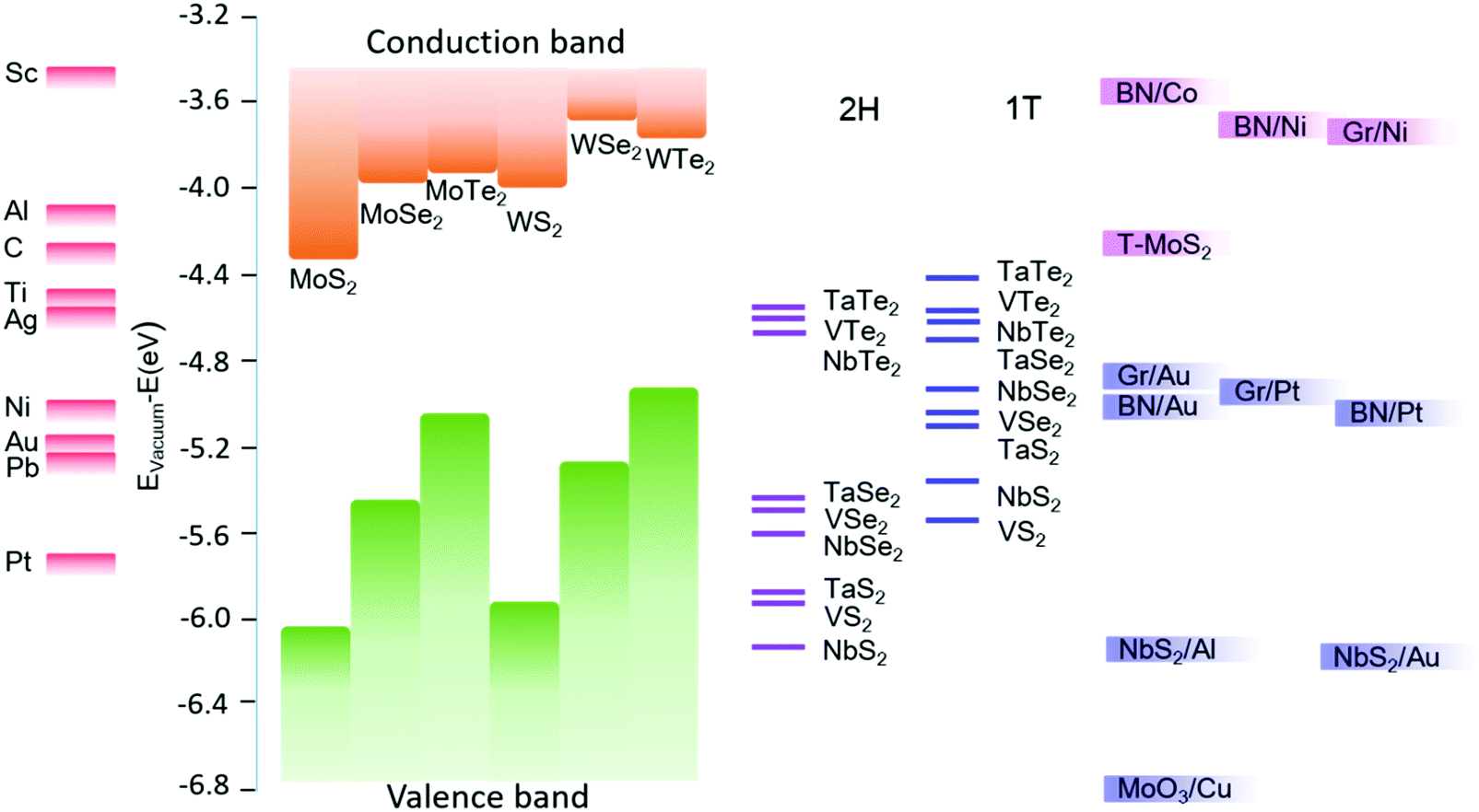 | ||
| Fig. 1 Band alignment of various TMDCs, elemental contact metals and metal/buffer contacts. The calculated work functions of p-type metal/buffer contacts are from ref. 29. The work functions of metals and the electron affinity and ionization potential of TMDCs are from ref. 30. | ||
Moreover, for the purpose of lowering the SBH and excluding the FLP effect, clean interfaces between metals and TMDCs are imperative. English et al. recently developed an ultra-high vacuum Au deposition method to obtain a high quality metal–MoS2 interface.31 The contact resistance is as low as 740 Ω μm at 300 K without intentional doping. As shown in Fig. 2a, Wang et al. demonstrated van der Waals (vdW) type bonding with no detectable chemical interactions formed between gold-capped indium (In) and monolayer MoS2 by using a standard electron-beam evaporator under a normal vacuum (<10−6 Torr) and thermal annealing at 200 °C.21 Through further characterization, the authors suggested that the procedure of depositing In and Au did not introduce any chemical reactions, distortions or strain at the metal/MoS2 interface. Undoubtedly, the excellent structural features of the vdW contacts with Au-capped In can lead to better transport performance. The extracted contact resistance of chemical vapor deposition (CVD)-grown monolayer MoS2 is about 3.3 ± 0.3 kΩ μm (at n = 5.0 × 1012 cm−2). Furthermore, by contrast, the contact resistances using pure Au deposited under an ultrahigh vacuum as electrodes are higher than In/Au at both room and low temperatures, as depicted in Fig. 2b. Besides MoS2, other 2D TMDCs such as WS2, WSe2 and NbS2 can also achieve low contact resistances by depositing In/Au. As implied by the transfer curves shown in Fig. 2c, WS2 devices with In/Au contacts exhibit lower contact resistance, larger drain currents and higher mobility compared with Ti contacts.
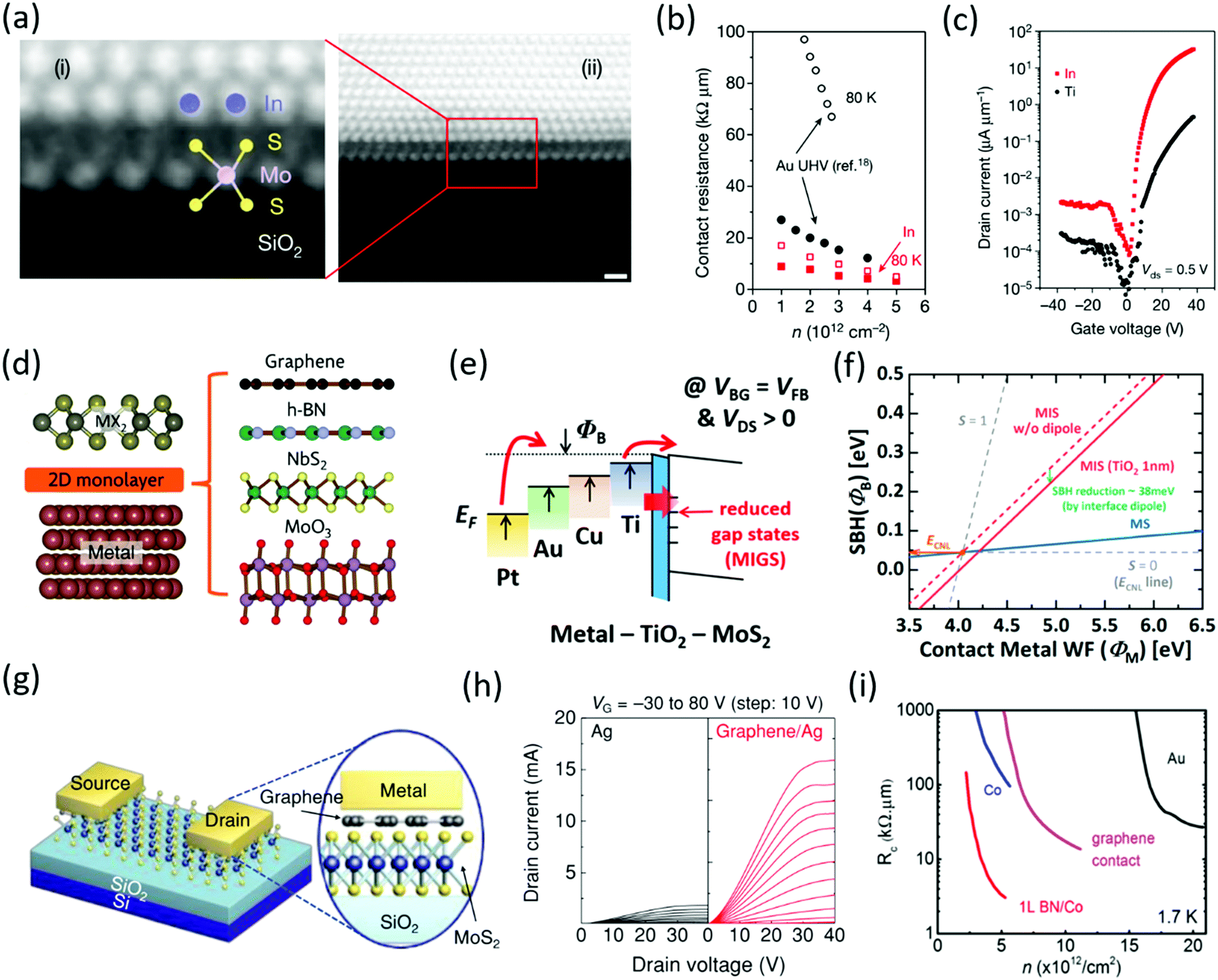 | ||
| Fig. 2 (a) Atomic-resolution images of In/Au on monolayer MoS2 (i) and a low-pass filtered ADF STEM image showing Mo, S and In/Au atoms (ii). (b) Contact resistance versus carrier concentration n for In/Au electrodes at room temperature (filled points) and at 80 K (open points). (c) Transfer characteristics of FETs with WS2 as the channel material and In/Au contacts; the length and width of the device are 1 μm and 1.2 μm at drain voltage Vds = 0.5 V. (a–c) Reproduced with permission.21 Copyright 2019, Springer Nature. (d) Side view of the metal/buffer/MX2 structure, M = Mo, W, X = S, Se, Te with possible buffer layers graphene, h-BN, NbS2, and MoO3. Reproduced with permission.29 Copyright 2016, Wiley-VCH. (e) Metal–TiO2–TMDC contact structures for four metal contacts under a flat-band bias condition. (f) Effective electron SBH under the flat-band bias condition of MS and MIS S/D structures for four metal contacts. Reproduced with permission.19 (e and f) Copyright 2018, American Chemical Society. (g) Schematic illustration of graphene interlayer-inserted MoS2 FETs with metal contacts. (h) Output characteristics of MoS2 FETs with Ag and graphene/Ag contacts. (g and h) Reproduced with permission.41 Copyright 2019, Wiley-VCH. (i) Comparison of h-BN tunneling Co contacts with different contact schemes in the literature. Reproduced with permission.43 Copyright 2017, American Chemical Society. | ||
Fermi-level depinning for TMDCs
In order to minimize the influence of interface states at the metal–TMDC interface and tune the SBH, inserting a buffer layer is a compelling way to break the interaction between the metal and TMDC layer, thus leading to Fermi level depinning and a low contact resistance. Recently, Farmanbar et al. predicted that inserting monolayer h-BN, graphene, MoO3 or NbS2 between a high work function metal such as Pt or Au and TMDCs leads to a low or zero SBH for TMDCs (Fig. 2d).29 Subsequently many researchers experimentally validated this prediction. Dankert and Chen et al. demonstrated that inserting a layer of TiO2 and MgO between Co/MoS2 contacts can significantly reduce the SBH from 120 meV to 27 meV and 60 meV to 10 meV, respectively.32,33 Likewise, Lee et al. reported that the SBH with a 1.5 nm-thick Ta2O5 inserted tunneling layer for MoS2 contacts was extracted as 29 meV, which is a significantly low value in comparison with that of ∼95 meV without the Ta2O5 inserted layer.34 As illustrated in Fig. 2e, the Fermi levels of the four contacts are strongly pinned close to the CNL of the MoS2 flake. However, when 1 nm-thick TiO2 is inserted at the interface between the metal and TMDC, the Fermi levels move closer to their ideal position by reducing interface states.19Fig. 2f shows the dependence of the effective electron SBH versus the work function of the contact metals with and without the TiO2 buffer layer. The pinning factor S of the metal–TMDC contact structures without the TiO2 buffer layer is about 0.02, suggesting that the Fermi level is strongly pinned at the interface. Inversely, the S value of the metal–insulator–TMDC contact structures with the TiO2 buffer layer is about 0.24, which indicates significant Fermi level depinning with the help of the TiO2 interlayer but still far from the Schottky–Mott rule.In addition, graphene can be introduced as a contact for 2D TMDCs due to its clean interface and high conductivity.35–37 Hong et al. demonstrated MoS2 FETs with a MoS2–graphene lateral heterostructure by the CVD method, showing improved electrical contact properties compared to their MoS2-only counterparts.38 However, the work function of graphene is typically higher than that of MoS2, leading to a higher SBH than conventional metals.39 Benefiting from the tunable Fermi level of graphene, metal–graphene–metal sandwich contacts were proposed to modulate the work function of graphene to achieve a zero SBH and low contact resistance.40 Therefore, it is expected that graphene/low work function metal structures can be employed as good contacts for 2D TMDCs. Chee et al. recently developed high-mobility MoS2 FETs with graphene/Ag contacts, as schematically illustrated in Fig. 2g.41 To further confirm the advantages of the graphene/Ag contacts, the electrical properties of the MoS2 FETs were investigated using three different contact metals (Ti/Au, Ag and graphene/Ag). The on-state current and field-effect mobility of the MoS2 FETs are significantly improved by factors of 5 and 10 using Ag contacts instead of Ti/Au owing to a lower work function of Ag and the hybridization of d-orbitals of Ag and MoS2. Moreover, when monolayer graphene was inserted between Ag and MoS2, the on/off current ratio and field-effect mobility of the MoS2 FETs are enormously enhanced from 7 × 10⁷ to 4 × 10⁸ and from 12 to 35 cm2 V−1 s−1 when compared with Ag contacts, as shown in Fig. 2h. The enhancement can be attributed to the low effective SBH between MoS2 and graphene/Ag contacts, leading to effective electron injection via graphene/Ag contacts. Besides the buffer layers mentioned above, Wang et al. suggested that inserted CVD grown 2D h-BN can reduce the SBH from 158 meV to 31 meV for Ni/MoS2 contacts.42 Cui et al. have experimentally demonstrated a robust contact scheme to the conduction band of monolayer MoS2 even at low temperatures (1.7 K) and low carrier density by inserting monolayer h-BN between Co and MoS2.43,44Fig. 2i displays the contact resistance versus carrier density at 1.7 K for the different contact methods.43 We can conclude that the inserted monolayer h-BN can significantly reduce the contact resistance of MoS2. By virtue of the low contact resistance of MoS2 at low temperatures, quantum oscillations at a carrier density as low as 3.5 × 1012 cm−2 can be clearly observed.
Edge contacts for 2D TMDCs
When the area of top contacts is restricted or limited, edge contacts can give more advantages than top contacts. In addition, the edges of multilayer TMDC flakes are exposed to form good contacts with metal electrodes because current can be injected into the layers and reduce the tunneling resistance formed by the vdW gap. It has been theoretically predicted that the orbital overlap is strong and a Schottky barrier does not exist in 1D edge contacts to TMDCs. Metal-induced gap states make the MoS2 in the vicinity of the contact metallic, thus leading to much more efficient charge carrier injection and lower contact resistance as compared to top contacts.45 Wang et al. first demonstrated a 1D edge contact to graphene by etching a stacked h-BN/graphene/h-BN heterostructure and then depositing metal on the edges of the graphene.46 However, this innovative approach seems not so effective for MoS2. Even though the current density is larger and the SHB at the edge-contact of metal–MoS2 is lower than that of top-contact, the contact resistance is larger. The main reason for the difference in contact resistance between MoS2 and graphene is that the transfer length of MoS2 is much larger than that of graphene, which causes insufficient efficiency of charge injection.47 Recently, Yang et al. have demonstrated that 1D edge contacts can give Fermi level depinning at the junction and simply control the polarity by applying low- or high-work function metal contacts without adhesion metal layers.48 The formation of the 1D edge contact was through SF6/O2 plasma etching on a h-BN/MoS2 heterojunction, as illustrated in Fig. 3a. A record high hole mobility of 432 cm2 V−1 s−1 at room temperature and an Ion/Ioff ratio exceeding 108 (Au–MoS2 1D edge contact) are successfully obtained. Furthermore, the pinning factor based on the 4 contact metals (Pb, Au, Mo and Ti) is obtained to be 0.975, which is very close to 1, indicating Fermi level depinning induced by the 1D edge contact. The reason can be given by the schematic band alignments of the 2D surface contact with large interface gap, vdW gap and 1D edge contact as shown in Fig. 3b. The physical separation between the metal and MoS2 is much smaller than the 2D surface contact, resulting in a reduction of the tunnel barrier widths and carrier transport loop. In this regard, the efficiency of carrier injection based on the 1D edge contact is higher than the 2D surface contact, which gives rise to Fermi level depinning at the metal–TMDC interface. Besides the 1D metal–TMDC edge contact, Guimaraes et al. developed a laterally stitched 1D graphene–TMDC edge contact through a scalable and patternable growth method.49Fig. 3c exhibits the comparison of the gate-dependent conductance of MoS2 using the 1D graphene–MoS2 edge contact and a conventional 2D metal–MoS2 top contact. The obvious enhancement of the two-probe conductance and field-effect mobility of MoS2 with the 1D graphene edge contact gives rise to a reduction of the contact resistance, implying a lack of a vdW gap or tunnel barrier as seen in the 2D top contact.50,51 Similarly, a 1D edge contact configuration on TMDC FETs can also be realized by direct growth of channel material from the edge of the predefined metal contact.52 The superior electrical performance of WSe2 with a 1D edge contact and density functional theory calculations indicate stronger metal–TMDC hybridization and more substantial energy gap states than the top-contact configuration.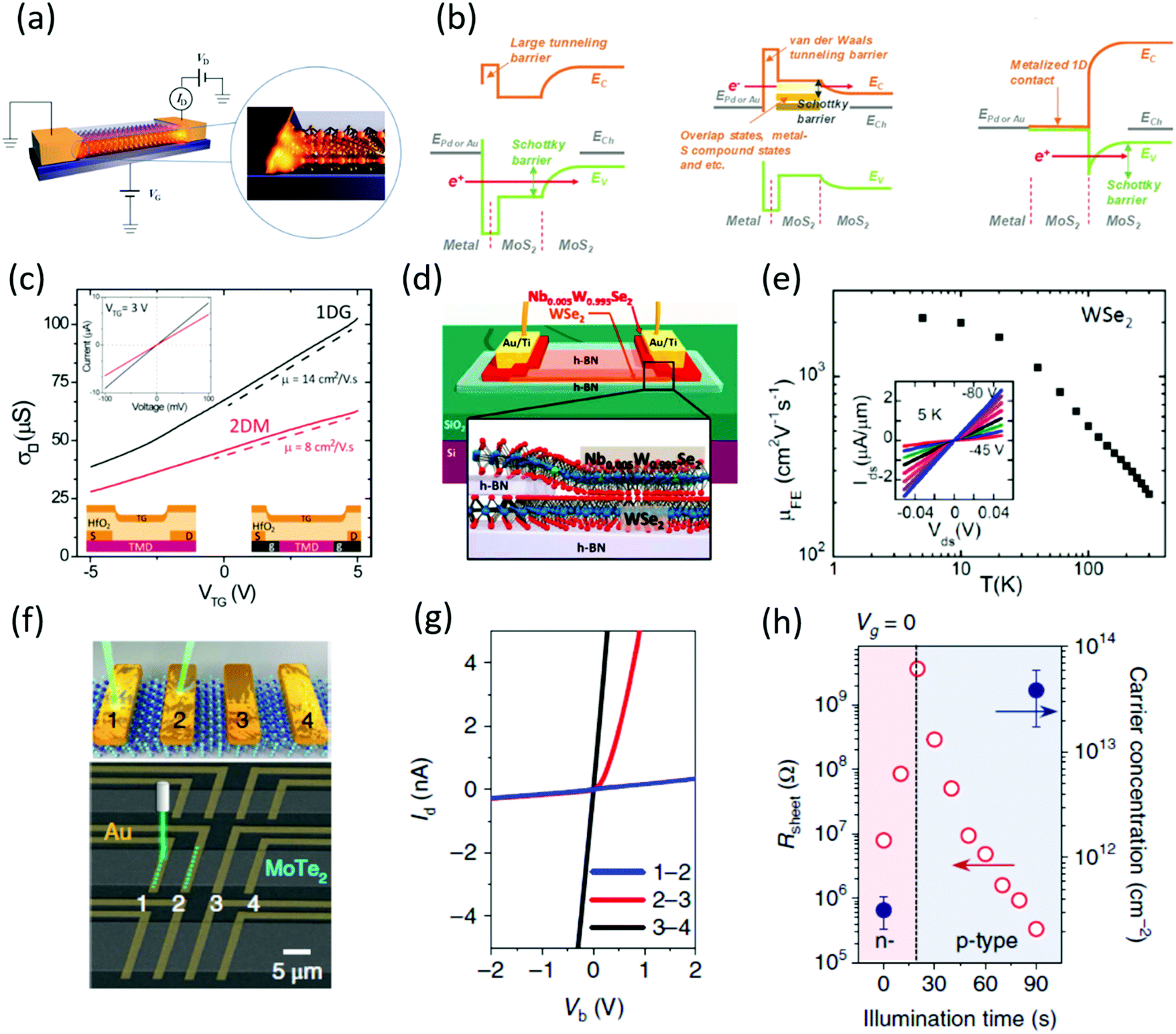 | ||
Fig. 3 (a) Schematic diagram of the 1D edge contact FET circuit with 1D edge schematic details. (b) Schematic band alignments of the 2D surface contact with large interface gap, van der Waals gap and 1D edge contact. (a and b) Reproduced with permission.48 Copyright 2018, Wiley-VCH. (c) Top gate voltage dependence of the two-terminal sheet conductance measured from MoS2 devices (length 22 μm and width 20 μm) with 1DG contacts (black curve) and with 2DM electrodes. Reproduced with permission.49 Copyright 2016, American Chemical Society. (d) Perspective side view of a WSe2 FET with degenerately p-doped WSe2 (Nb0.005W0.995Se2) contacts. (e) Two-terminal field-effect hole mobilities in WSe2 as a function of temperature. (d and e) Reproduced with permission.54 Copyright 2016, American Chemical Society. (f) SEM image of MoTe2 back-gated FET devices. (g) I–V characteristics of each channel with pairs of contacts 1-2 (blue line), 2-3 (red line) and 3-4 (black line). (h) Variation in the channel sheet resistances and carrier concentrations with illumination times from 0 to 90![[thin space (1/6-em)]](https://www.rsc.org/images/entities/char_2009.gif) s. (f–h) Reproduced with permission.55 Copyright 2018, Springer Nature. s. (f–h) Reproduced with permission.55 Copyright 2018, Springer Nature. | ||
Strong orbital overlaps, absence of a SB, and lower tunnel barriers are all advantages of edge-contact configurations compared to top contacts. Hence, edge-contact configurations have a higher capability of electron injection and thereby decrease the contact resistance. Considering the contact area (current), a mixed (top and edge) contact configuration may be better.
Doped contacts for TMDCs
Doping is another approach for contact engineering. The width of the Schottky barrier at the metal/TMDC interface can be extremely reduced by heavily doping, leading to more efficient carrier injection and low contact resistances. Fang et al. demonstrated that NO2 molecules are good candidates for degenerate p-type surface dopants of WSe2.53 A WSe2 FET using the NO2 surface strategy exhibits excellent performance with a hole mobility of ∼250 cm2 V−1 s−1, a low subthreshold swing (SS) of ∼60 mV dec−1, and an on–off current ratio higher than 106 at room temperature. Chuang et al. reported a universal method for low and ohmic contacts for TMDCs using assembly of appropriate doped TMDCs as S/D contacts as illustrated in Fig. 3d.54 The contact resistance of a few-layer WSe2 FET is as low as 0.3 kΩ μm and the on–off current ratio is as high as 109. Moreover, the contact at low temperatures is also ohmic and the field-effect hole mobility increases from 200 cm2 V−1 s−1 at room temperature to 2000 cm2 V−1 s−1 at cryogenic temperatures as presented in Fig. 3e. Recently, Seo et al. surprisingly found that a focused laser beam could also induce p-doping in MoTe2 when the light locally illuminates Au electrodes on 2H-MoTe2.55Fig. 3f shows the schematic of the device and process of doping. Through investigations of scanning tunneling microscopy and spectroscopy (STM/STS), they concluded that local light illumination induces Mo vacancies, followed by on-site chemical absorption of oxygen clusters, which results in local p-doping in 2H-MoTe2. In order to further confirm this type of p-doping, the I–V characteristics of channels with pairs of contacts 1-2, 2-3, and 3-4 were measured, which are shown in Fig. 3g. The rectifying characteristics of the I–V curves of channel 2-3 indicate the existence of p–n diodes. At the same time, the transfer curve of channel 1-2 exhibits p-type transportation as well. Since the local p-doping induced by light illumination is associated with molecule-vacancy clusters, the illumination time can simply modulate the doping profile. As plotted in Fig. 3h, the hole concentration is drastically enhanced with an increase of the illumination time until the contact becomes degenerate. Lately, Tutuc's and Ensslin's groups have developed a new method to achieve ohmic contacts for MoS2 and WSe2 even at low temperatures through drastically enhancing the concentrations of carriers of TMDCs by modulating both back and top gates of the device.56–58 With the help of excellent ohmic contacts of TMDCs at low temperatures, SdH oscillations and the quantum hall effect of TMDCs could be observed, suggesting rich, novel and unpredicted physics in the system of TMDCs.Phase engineering and metal transfer for TMDCs
It is well known that typical TMDCs usually possess both metallic and semiconducting phases. The phase transition of TMDCs from 2H to 1T can be realized by several methods, such as electrostatic doping,59 laser irradiation,60 strain,61 chemical treatment,62 and plasma treatment.63 In addition, thickness modulation owing to the strong interlayer interaction would also lead to distinct property tuning.64,65 Zhao et al. reported a layer-dependent semiconductor-to-semimetal evolution of 2D layered PtSe2, which is only dependent on the layer number.64 In 2014, Kappera et al. improved the contact performance of MoS2 by using local phase engineering.62 They employed an organolithium chemical method to obtain metallic 1T-MoS2, which is used as S/D contacts. The low contact resistance of 200–300 Ω μm at zero gate bias resulted from the 1D atomically sharp edge contact and the similar work functions of the 1T and 2H phases. In 2015, Cho et al. used laser illumination to locally transform semiconducting 2H-MoTe2 to metallic 1T′-MoTe2.60 The field-effect carrier mobility of the MoTe2 device is significantly enhanced by a factor of about 50 with contact of 1T′-MoTe2 and the SBH is greatly reduced by a factor of about 20 in comparison with the conventional 2H-MoTe2 device. Moreover, Lee et al. recently presented epitaxial vdW contacts by vertical epitaxy of metallic 1T′-WTe2 on semiconducting 2H-WSe2.66 This device possesses ambipolar transfer curves with higher mobility and on–off current compared with conventional top contacts. The SBH of epitaxial vdW contacts for WSe2 extracted from temperature-dependent transfer curves is as low as 70 meV, which indicates efficient carrier injection and low contact resistance as mentioned above. In the same way, Leong et al. epitaxially stitched metallic VS2 and semiconducting MoS2 to form lateral heterostructures through CVD growth.67 The SBH of the lateral VS2–MoS2 device extracted from the temperature-dependent electrical properties is as small as about 30 meV, giving rise to 6-fold enhanced field-effect mobility of monolayer MoS2 with top Ni contacts. In addition, the contact resistance of the lateral VS2–MoS2 device is as small as 520 Ω μm at Vg = 50 V, which is one order smaller than the conventional Ni top contact. Recently, Sung et al. introduced a CVD technique to epitaxially fabricate coplanar polymorphic heterostructures by combining with 2H-MoTe2 and metallic 1T′ MoTe2.68 The schematic illustration and the optical microscope image of the as-grown 1T′–2H–1T′ MoTe2 polymorph device are shown in Fig. 4a and b. By comparing the I–V and transfer curves as depicted in Fig. 4c and d, it can be found that not only is the conductance with the 1T′-coplanar contacts two orders of magnitude higher than the conventional Au-top contact FET, but also more effective gate modulation is obtained in the 1T′-coplanar contact FET. The reason for this is that the interface at the 1T′-coplanar contact is covalently bonded with atomic precision without forming Schottky barriers as for the Au-top contact. The experimentally extracted SBH of the 1T′-coplanar contact FET is merely 22 meV, which is approximately one order lower than the Au-top contact FET. Likewise, Zhang et al. reported a similar result of a low contact barrier in a 2H–1T′ MoTe2 in-plane heterostructure synthesized by chemical vapor deposition.69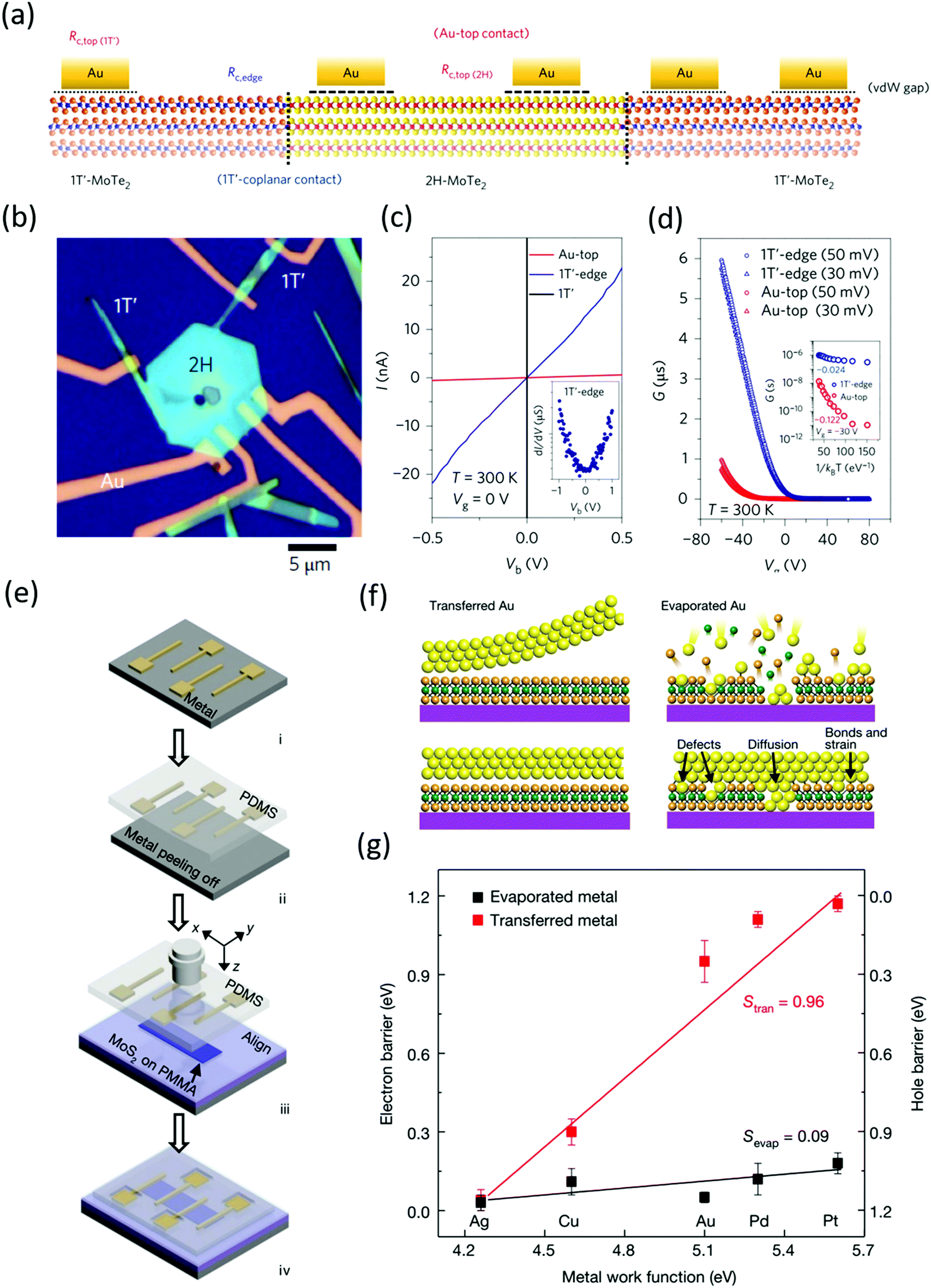 | ||
| Fig. 4 (a) Illustration of the MoTe2 polymorph device, containing three different types of contact: coplanar 1T′–2H polymorphic contact Rc,edge, Au-top contact to 2H channels Rc,top and Au-top contact to 1T′ MoTe2 metals. (b) Optical microscope image of a 1T′–2H–1T′ MoTe2 polymorph device. (c) Current–voltage (I–Vb) curves at 300 K for 1T′-coplanar contacted (blue), Au-top contacted (red) 2H MoTe2 transistors and Au-top contacted 1T′-MoTe2 (black). (d) Transfer characteristics of back-gate voltage Vg modulation of sheet conductance G for 1T′-coplanar contacted (blue), and Au-top contacted (red) 2H-MoTe2 FETs. (a–d) Reproduced with permission.68 Copyright 2017, Springer Nature. (e) Schematic illustrations of vdW integration of metal–semiconductor junctions: (i) metal deposition on a sacrificial substrate; (ii) peeling off the metal; (iii) alignment; and (iv) contact lamination and probe window opening. (f) Cross-sectional schematics of the transferred Au electrode on top of MoS2 and conventional electron-beam-deposited Au electrodes on top of MoS2. (g) For transferred metal electrodes, the majority carrier type and corresponding Schottky barrier height are strongly dependent on the metal work function with a slope (S = 0.96) approaching unity, suggesting excellent obedience to the Schottky–Mott law. With conventional evaporation-deposited metal electrodes, the devices invariably show n-type behaviour with a small electron Schottky barrier and a slope S = 0.09, indicating a strong pinning effect at the metal–semiconductor interface. (e–g) Reproduced with permission.70 Copyright 2018, Springer Nature. | ||
Conventionally depositing contacts of metal may introduce contamination at the metal/TMDC interface during lithography steps and produce physical damage to the surface of TMDCs, leading to poor contacts that eventually degrade the device performance. Recently, Liu et al. reported a technique of creating vdW metal–semiconductor junctions by transferring pre-fabricated metal electrodes onto dangling-bond-free TMDCs.70 The procedure of this method is shown in Fig. 4e. In comparison with the conventional technique of evaporating metal with top contact, this method could avoid chemical disorder and defect-induced gap states, which is schematically illustrated in Fig. 4f. As plotted in Fig. 4g, the extracted value of S for transferred metal is much larger than that for evaporated metal with top contact, indicating Fermi level depinning at the metal/TMDC interface. Moreover, the fitted value of S for the transferred metal is about 0.96, which is much larger than those of Si and GaAs and approaches the limit of the Schottky–Mott law defined by electrostatic energy alignment.71,72 In this regard, the method of transferred metal on TMDCs can definitely produce a nearly ideal interface without inevitable chemical disorder and gap states and modulate the SBH by transferring different metals. Despite Liu's method, Jung et al. also developed a similar transferred contact approach by dry transferring metal-embedded h-BN onto the surface of TMDCs.73 This approach prevents direct-metallization-induced damage and contamination during the fabrication process. Electrical measurements prove that the transferred devices have low contact resistance at both room and low temperatures without forming a Schottky barrier at the interface of metal/TMDC.
3. Channel engineering for TMDCs
2D layered TMDCs possess great potential for future channel materials in transistors. Owing to their atomic body thickness, 2D TMDCs are very sensitive to the interface properties.6,74–76 Therefore, channel interface engineering plays a predominant role in modulating the properties and improving the device performance of 2D TMDCs. Here, we review the recent developments in channel engineering of 2D TMDCs, including dielectric engineering, ion implantation treatment, surface plasma treatment and surface charge transfer doping, etc.Dielectric engineering for TMDCs
The experimental mobilities for 2D TMDC based transistors are usually lower than the theoretical values, which is partially due to the extrinsic scattering caused by defects, traps and impurities at the interface. Dielectric engineering, as an effective way to suppress extrinsic scattering, such as phonon scattering and charge impurities, can significantly improve the performance of 2D based devices.16,77,78 Commonly used dielectrics include inorganic non-metallic materials, such as SiO2, Al2O3, HfO2, etc., and some polymers, such as PMMA, PVA, PVDF, etc.79 Radisavljevic et al. adopted high-k HfO2 as the dielectric with monolayer MoS2 and achieved a high mobility of ∼200 cm2 V−1 s−1 owing to the effective screening of Coulomb scattering by the high-k HfO2.80,81 h-BN, which is one kind of 2D insulator with atomic smoothness, is widely used in TMDC devices via constructing vdW structures.82–86 Chan et al. utilized 2D h-BN to design a back-gated bilayer MoS2 FET, and suggested that the field effect mobility of the device with h-BN as the dielectric is greatly improved compared with SiO2, resulting from a lower interface trap density between MoS2 and h-BN.87 In addition, Liu et al. obtained a high field effect mobility of 1300 cm2 V−1 s−1 for monolayer MoS235 and Cui et al. 34000 cm2 V−1 s−1 for six-layer MoS2 at low temperature by using graphene electrodes and h-BN encapsulation.44 Very recently, Illarionov et al. demonstrated that epitaxial calcium fluoride (CaF2) can serve as an ultrathin dielectric for 2D TMDCs by forming a quasi vdW interface with 2D TMDCs.88 Besides TMDC based transistors, Li et al. demonstrated a p-MoTe2/graphene/n-SnS2 photodetector encapsulated by h-BN schematically shown in Fig. 5a.89 The fabricated p-MoTe2/graphene/n-SnS2 photodetector exhibits a high rectification ratio, a high photo-responsivity exceeding 2600 A W−1 and a fast light response speed (Fig. 5b and c).
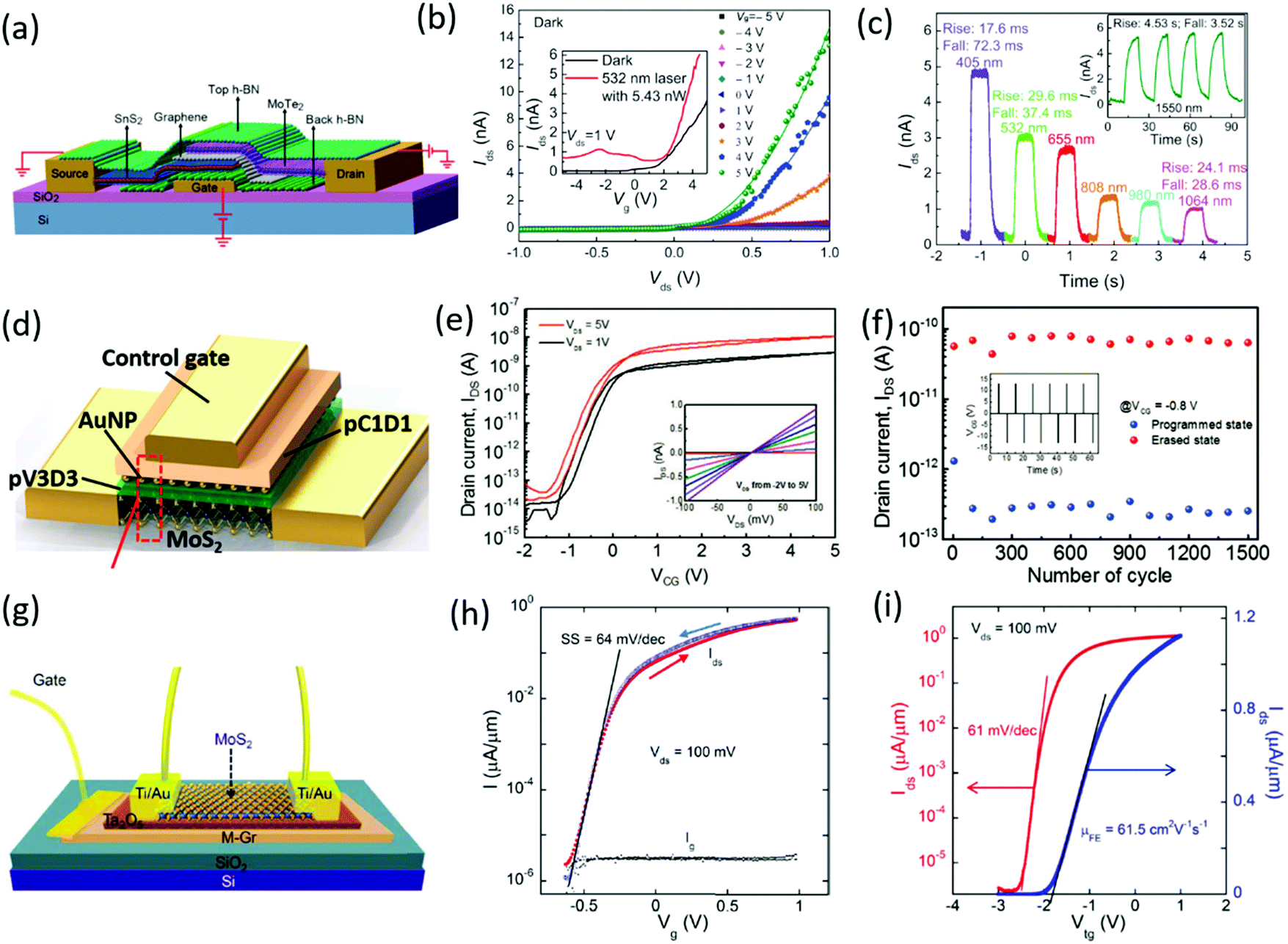 | ||
| Fig. 5 Dielectrics tuning the properties of 2D TMDCs. (a) The diagram of the device based on a p-MoTe2/graphene/n-SnS2 heterostructure. (b) I–V curves under different gate voltages of the device. (c) Light response I–t curves of the photodetector. (a–c) Reproduced with permission.89 Copyright 2019, Wiley-VCH. (d) Schematic illustration of the fabricated MoS2 based memory device. (e) Transfer curves of the MoS2 FET. (f) Cycling endurance result of a C-memory device for 1500 cycles. (d–f) Reproduced with permission.94 Copyright 2019, Wiley-VCH. (g) Schematic diagram of the Ta2O5 dielectric 2D MoS2 based FET. (h) I–V curves under different gate voltages. (i) Transfer curve of the MoS2 FET. (g–i) Reproduced with permission.95 Copyright 2017, IOP Publishing. | ||
By choosing appropriate dielectrics, the performance of TMDCs can be further engineered. Bao et al. analyzed the mobility of MoS2 transistors on different dielectrics (SiO2 and PMMA) and found that the MoS2 devices on the SiO2 substrate show an n-type transport characteristic with an electron mobility of 30–60 cm2 V−1 s−1, while the MoS2 transistors on the PMMA substrate exhibit ambipolar transport behavior with electron and hole mobility up to 470 and 480 cm2 V−1 s−1.90 Feng et al. also employed PMMA in InSe transistors and achieved a high mobility of 1055 cm2 V−1 s−1 for the device on PMMA-coated Al2O3, which is significantly improved compared with that of 64 cm2 V−1 s−1 without PMMA.91 It is found that the PMMA layer can effectively screen the hydroxyl groups, water, or other chemical absorptions of the oxidized dielectric substrates, suppressing the carrier scattering from interfacial coulomb impurities or surface polar phonons.75 In addition, organic based self-assembled monolayers (SAMs) have also attracted much attention in terms of similarly suppressing scattering effects for 2D materials.92 Recently, Kawanago et al. fabricated a 2D MoS2 FET with n-octadecylphosphonic acid (ODPA), which is a phosphonic acid-based SAM, and achieved a low SS of 69 mV dec−1.93 As illustrated in Fig. 5d, Yang et al. introduced a hybrid layer including a poly(1,3,5-trimethyl-1,3,5-trivinyl cyclotrisiloxane) (pV3D3) tunneling dielectric, Au NP floating gate, and pC1D1 (2-cyanoethyl acrylate:di(ethylene glycol)divinyl ether = 78:22 from a 1:1 flow rate ratio) blocking dielectric layer to design a MoS2 memory device.94 As shown in Fig. 5e and f, the device exhibits a high on/off ratio of 106, low operating voltages (∼13 V), stable retention times exceeding 105 s and cycling endurance exceeding 1500 cycles.
Moreover, some oxide dielectrics directly synthesized on 2D original TMDCs can also be adopted for TMDC transistors. Chamlagain et al. converted 2D TaS2 to Ta2O5 flakes by thermal oxidation and used the resultant Ta2O5 as the gate dielectric for a 7 nm-thick MoS2 transistor, as shown in Fig. 5g.95 Corresponding XPS and AFM results indicate that the Ta2O5 is uniform and the capacitance–voltage measurements suggest a high dielectric constant of ∼15.5 for Ta2O5. The device with Ta2O5 as the gate dielectric shows high performance with an electron mobility of 60 cm2 V−1 s−1, high on/off ratio of 106 and low SS of 61 mV dec−1 as exhibited in Fig. 5h and i. In addition, employing negative capacitance in 2D TMDC transistors can further lower the SS beyond the thermionic limit.96–98 Si et al. reported the first MoS2 based negative capacitance transistor using ferroelectric hafnium zirconium oxide (HZO) as the dielectric and obtained a SS lower than 60mV dec−1 at room temperature.96 Similarly, Liu et al. used the ferroelectric P(VDF-TrFE) as the dielectric and achieved a SS of 42.5mV dec−1.97
Surface treatment for TMDCs
The properties of atomically 2D materials can be further tailored via surface treatment such as electron irradiation, ion implantation, plasma treatment, etc.99–103 Ion implantation is one commonly used effective means to achieve doping for bulk semiconductors, but it is difficult to obtain a similar effect in atomically thin TMDCs. On the other hand, the use of ion beams is able to create defects and thin the thickness of 2D materials,101,104,105 which is of great importance for the preparation process and performance tuning of 2D materials. Guo et al. introduced 209Bi ions to irradiate few-layer MoS2; an increase in the O 1s component and the appearance of higher oxidized Mo6+ in XPS spectra and a blue shift of the A1g phonon mode in Raman with a dose increase of the 209Bi ion irradiation are observed, suggesting that ion irradiation induces O2 adsorption and causes decreasing electrons in MoS2, resulting in p-type doping.106 Similarly, immersing few layer MoS2 in Hg2+ ions would also produce a p-type doping effect, which can be used as a sensor to detect Hg2+.107 More visual means of characterization were also used to study the variation of 2D TMDCs under ion irradiation. For instance, an increase of atomic defects in 2D MoSe2 with increasing He+ irradiation dose was investigated by scanning transmission electron microscopy (STEM),108 and a monocrystal–amorphous transformation in He+ irradiated 2D MoS2 was observed by TEM.109Bertolazzi et al. modulated the numbers of sulfur vacancies in single-layer MoS2 transistors through low-energy argon-ion irradiation.110 The mobility of the MoS2 transistor drops from 25 to 8 cm2 V−1 s−1 with an ion fluence of 8.2 × 10¹² ions per cm2. Interestingly, a significant recovery of these created defects was demonstrated with a new chemical treatment based on vapors of short thiol-terminated molecules. Similarly, Liu et al. control the density of Se vacancies in monolayer WSe2via Ga ion irradiation, which is schematically shown in Fig. 6a.111 The atomic ratio of Se and W is significantly reduced with an increase of the Ga ion irradiation dose (Fig. 6b) and the current is increased after Ga ion irradiation (Fig. 6c). Furthermore, the photo response performance of the WSe2 device including the response speed and range was also enhanced. In addition, Cheng et al. investigated the effect of the energy of focused Ar+ ion beam irradiation on the structure and properties of MoS2 (Fig. 6d).112 The contact resistance of the device drops from 17.5 kΩ μm to 6 kΩ μm under 60 eV Ar+ ion irradiation for 3 s with an ion dose of 5.4 × 10¹² ions per cm2 (Fig. 6e). Based on the transfer curves under varying ion energy, optimal device performance was achieved under 60 eV Ar+ ion irradiation as shown in Fig. 6f. Moreover, by selective ion irradiation of a single TMDC flake, homo-junctions can be easily obtained. Previously, a homo-junction based on 2D WSe2 was constructed by using He+ ion irradiation and a significant photovoltaic effect was observed.113
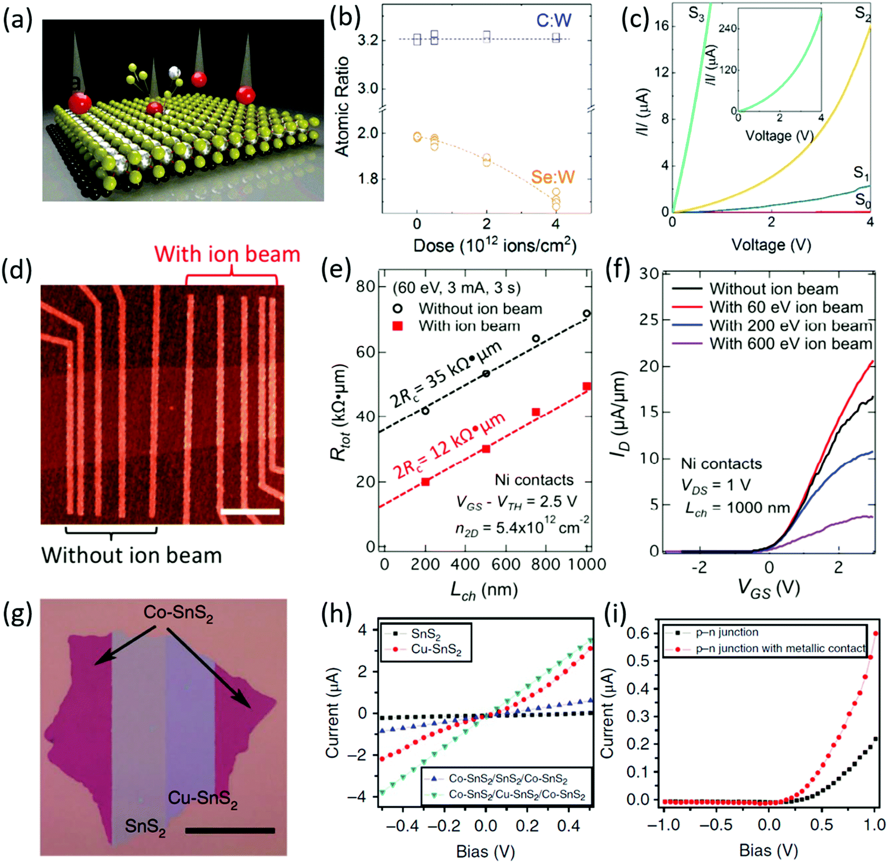 | ||
| Fig. 6 Ions modulate the transport behavior of 2D TMDCs. (a) Schematic diagram of the Ga ion irradiation of 2D WSe2. (b) The atomic ratio as a function of the Ga ion irradiation dose. (c) The ID–VD curves of the vertical graphene/WSe2 heterostructures with various irradiation time. Reproduced with permission.111 Copyright 2018, American Chemical Society. (d) AFM image of MoS2 devices with two regions. (e) The contact resistance of the device with and without ion irradiation. (f) Effect of different ion beam energies on the device performance. Reproduced with permission.112 Copyright 2019, IOP Publishing. (g) Optical image of the sample seamlessly integrating n-type SnS2, p-type Cu–SnS2 and metallic Co–SnS2. (h) I–V curves of SnS2 or Cu–SnS2 with a Ti/Au electrode. (i) Typical rectification behavior of the SnS2/Cu–SnS2 heterojunction. Reproduced with permission.114 Copyright 2018, Nature Publishing Group. | ||
Although the traditional ion implantation technique is difficult to employ in ultrathin 2D materials, similar attempts have been conducted. Lately, Gong et al. developed an ion doping method by solvent-based intercalation,114 where tetrakis (acetonitrile) copper hexafluorophosphate and dicobalt octacarbonyl acetone solution was used to dope Cu and Co ions into bilayer SnS2. Color contrast in the optical image can be observed after doping (Fig. 6g) and the intercalation of Cu and Co atoms was further confirmed by HRTEM. It is found that the Cu doped SnS2 transistor shows a p-type characteristic with a hole mobility of 40cm2 V−1 s−1, while the Co doped device shows a metallic behavior. In addition, an ohmic contact between SnS2 and Co–SnS2 was demonstrated from the I–V curves (Fig. 6h) and typical rectification behavior of the SnS2/Cu–SnS2 junction in Fig. 6i was clearly observed. Such ion doping can be used to construct p–n diode and seamless electrode contacts.
Plasma treatment, which is a commonly used method of substrate cleaning, thickness thinning and materials etching, can be adopted in assisting materials synthesis, patterning, and precisely controlling the layer number for 2D TMDCs.100,115 Layer by layer thinning of 2D TMDC flakes by Ar, N2 and O2 plasma can be achieved by controlling the plasma energy.116–118 Using such a strategy, Shim et al. demonstrated enhanced photoelectric performance of a 2D ReS2 device for a thinner sample.119 In addition, high energy plasma treatment can be used to pattern 2D TMDCs and construct heterostructures,120 while low energy plasma treatment is suitable for doping and defect engineering.121–124 Recently, Jadwiszczak et al. used O2/Ar plasma to modulate the carrier mobility of a few-layer MoS2 FET,125 and found that the treatment time plays an important role for the device performance. When the exposure time is 6 s, the current is significantly increased, while the current is almost decreased to zero when the plasma treatment is 12 s (Fig. 7a). The transfer curves in Fig. 7b demonstrate an obvious shift of the threshold voltage with varying plasma treatment. The maximum mobility is decreased with an increase of the plasma treatment time as shown in Fig. 7c, while a higher mobility in the gate bias region between −40 V and 5 V is obtained for the sample with 6 s plasma treatment. It is revealed that a transient 2D substoichiometric phase of molybdenum trioxide (2D-MoOx) can be formed in the plasma treatment process, modulating the electronic behavior of MoS2. Additionally, Cho et al. introduced O2 plasma to modulate the contact between Pt and MoTe2 (Fig. 7d).126 The exposed MoTe2 contact region was treated with 60 s O2 plasma before metal deposition, where a layer of MoOx was formed. With O2 plasma treatment, the device performance is dramatically improved, as shown in Fig. 7e and f. The mobility is as high as 63 cm2 V−1 s−1, which is significantly higher than the device without O2 plasma treatment. For some particular TMDCs, plasma treatment can be used to create a dielectric layer to improve the device performance. Lai et al. controllably converted 2D semiconducting HfS2 into insulating HfO2 by using O2 plasma treatment (Fig. 7g).127 By extending the process duration, the HfS2 can be completely oxidized to HfO2 (Fig. 7h). Based on such plasma treatment, a top-gated HfS2 FET using HfO2 as the dielectric is fabricated, showing a high on/off current ratio of 107 and an electron mobility of 10 cm2 V−1 s−1 (Fig. 7i). Such a method is of great significance in constructing the lateral junction and device integration for 2D TMDCs.128,129
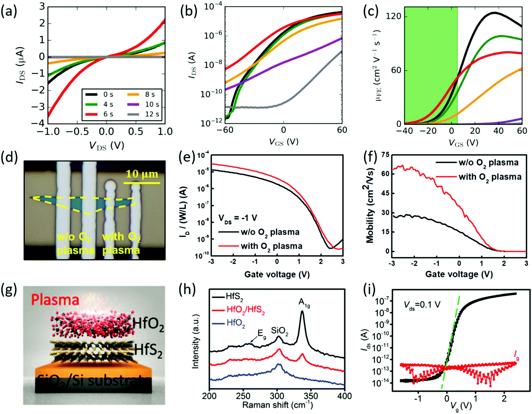 | ||
| Fig. 7 Plasma modulates the transport behavior of 2D TMDCs. (a) Effect of the O2/Ar (1:3) plasma exposure time on the I–V curves. (b) Transfer curve and (c) mobility–Vg curves of a 4L MoS2 based FET. Reproduced with permission.125 Copyright 2018, AAAS. (d) Optical image of the 2D MoS2 device with and without O2 plasma treatment. (e) The transfer curve and (f) mobility as a function of gate voltage of the device with and without O2 plasma treatment. Reproduced with permission.126 Copyright 2018, Wiley-VCH. (g) Schematic diagrams of the HfO2/HfS2 heterostructure created by O2 plasma treatment. (h) Raman spectra of the HfS2, HfO2/HfS2 and HfO2. (i) The transfer curve of the device based on the HfO2/HfS2 heterostructure. Reproduced with permission.127 Copyright 2018, Royal Society of Chemistry. | ||
Surface charge transfer doping for TMDCs
Surface charge transfer doping (SCTD), which is a commonly used non-destructive means for regulating the properties of semiconductors, has attracted tremendous attention for varying 2D materials.130–132 Park et al. investigated the interaction between DNA and MoS2 and found that the phosphate backbone (PO4−) in DNA would lead to n-doping for MoS2, while M-DNA, which is DNA slightly modified by metal ions (Zn2+, Ni2+, Co2+, and Cu2+), would result in p-doping owing to the positive dipole moments in these metal ions, which reduce the electron carrier density in MoS2.133 Tongay et al. reported over 100 times enhancement of the PL intensity of MoS2 by physical adsorption of O2 and H2O molecules, which is totally different from the case of inert gases where such an effect is not observed.134 It is suggested that the physisorbed electronegative O2 and H2O molecules on MoS2 and MoSe2 would weaken the electrostatic screening and destabilize excitons, eventually leading to the enhancement of PL. In addition, they observed the opposite effect of molecular physisorption for p-type WSe2. Kiriya et al. demonstrated the doping effect of benzyl viologen (BV), which has a high reduction potential, on MoS2 and obtained a high electron sheet density up to 1.2 × 1013 cm−2.135 Du et al. investigated the doping effect of polyethyleneimine (PEI) on multilayer MoS2 transistors and achieved a 2.6 times reduction in sheet resistance and 1.2 times reduction in contact resistance.136 In addition, surface modification with C60 and MoO3 layers, Cs2CO3 and amorphous titanium suboxide (ATO) has also been employed to realize doping for 2D MoS2.137–139 It is noteworthy that solid-state oxide doping for TMDCs via SCTD offers a promising CMOS-compatible process for applications in ICs.140Moreover, the SCTD strategy can be also applicable for other 2D materials. Li et al. employed indium layers as dopants for layered InSe transistors as shown in Fig. 8a.141 A high electron mobility of 3700 cm2 V−1 s−1 at room temperature is obtained with good stability, which can be attributed to enhanced electron-doping at the In/InSe interface (Fig. 8b and c). Lim et al. have investigated the n-doping effect of α-MoTe2via atomic-layer deposited Al2O3, as illustrated in Fig. 8d.142 The transfer curve of the pristine α-MoTe2 transistor shows a p-channel characteristic while that of the α-MoTe2 transistor with Al2O3 exhibits clear n-channel behaviors (Fig. 8e and f). They further construct a CMOS inverter based on single α-MoTe2 flake, showing a high DC voltage gain of 29 and a low static power consumption of a few nanowatts. To achieve p-doped MoS2, both Choi et al.143 and Liu et al.144 adopted an AuCl3 layer on the surface of MoS2via spin coating. A high hole mobility of 68 cm2 V−1 s−1 at room temperature of p-doped MoS2 is obtained, owing to effective electron transfer from the MoS2 to the AuCl3 layer.144 Besides, other dopants such as fluorine-rich molecules,145 and InGaZnO film146 have also been attempted to realize p-doping in 2D MoS2.
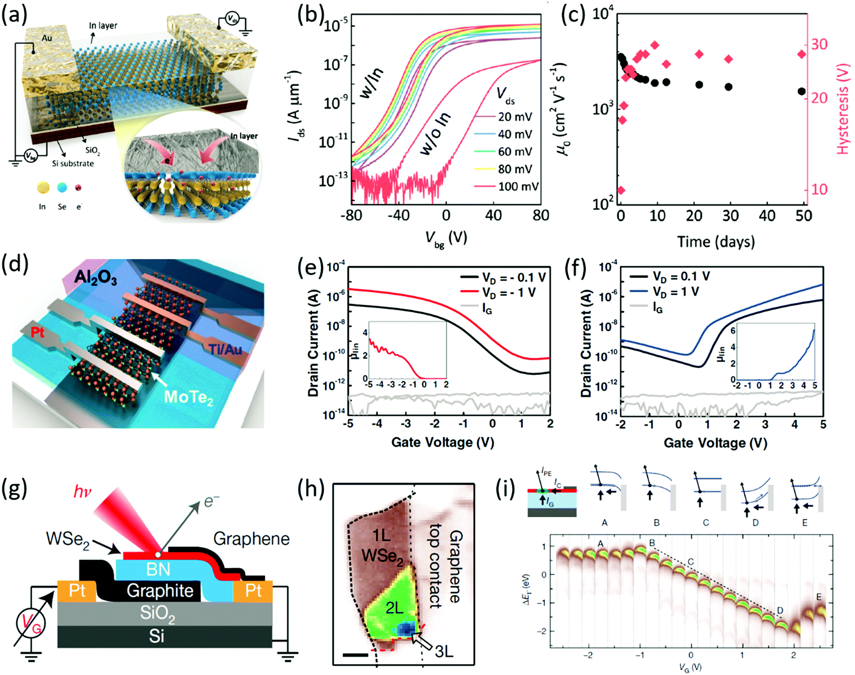 | ||
| Fig. 8 Surface charge transfer modified 2D TMDCs. (a) Schematic illustration of the back-gate InSe FET, packaged with an In layer as protective encapsulation and a surface dopant for the layered InSe channel. (b) The transfer curves of the InSe FET. (c) Time evolution of the mobility and the hysteresis of the InSe FET with an In layer. Reproduced with permission.141 Copyright 2018, Wiley-VCH. (d) Schematic illustration of a selective ALD doped MoTe2 device. (e) The transfer curves of the device covered with Al2O3. (f) The transfer curves of the device without Al2O3. Reproduced with permission.142 Copyright 2017, Wiley-VCH. (g) Diagram of a WSe2/h-BN/graphene device. (h) Scanning photoemission microscopy images of the WSe2 device. (i) The effect of the gate voltage on the Femi level and bandgap of WSe2. Reproduced with permission.148 Copyright 2019, Nature Publishing Group. | ||
In addition, some 2D TMDCs such as WSe2 often exhibit ambipolar performance, suggesting that both n- and p-doping can be achieved by simply coupling different gate voltages. Li et al. created a WSe2 p–n diode in a vertical stacked WSe2/h-BN/graphene structure with a semifloating gate field-effect transistor configuration,147 showing a good rectification ratio of 104. In regard to visualizing the SCTD behavior, Nguyen et al. recently suggested that micrometre-scale, angle resolved photoemission spectroscopy applied to vdW heterostructures enables the observation of the change of Fermi level and band structure when a gate voltage is applied.148 By using such a method, they successfully measured the changes of electronic bands during the electrostatic gating doping of monolayer WSe2 (Fig. 8g–i). Such a technique may also open up a powerful and controllable way to investigate the SCTD mechanism for 2D TMDCs.
4. Interface engineering of TMDCs for electronic devices
2D layered TMDCs with unique electronic properties have aroused tremendous interest for applications in electronic devices including diodes, transistors, circuits, memories, etc. Employing both contact and channel engineering for 2D layered TMDCs enables manipulating their properties in a controllable manner, optimizing the device performances and further fulfilling the requirements for future functional electronics.TMDC based diodes
Atomically thin TMDC based diodes are the fundamental building blocks for many advanced functional electronics. Usually, 2D layered TMDCs are hole- or electron-dominated, making it difficult to realize homogeneous electronics. Surface engineering has been emerging as an efficient method for realizing reliable doping in layered TMDCs.149–152 Zheng et al. demonstrated a homogeneous p–n MoSe2 diode via selectively MoSe2 doping through ultraviolet-ozone treatment, which effectively tunes n-type few-layer MoSe2 to p-type.149 In addition, by sequential treatment of a single MoSe2 flake with air rapid thermal annealing for p-doping and triphenylphosphine (PPh3) solution coating for n-doping, Fan et al. also successfully fabricated a lateral MoSe2 p–n homojunction, which shows a relatively high rectification ratio of 104.151 Chen et al. reported a monolayer WSe2 homojunction on the ferroelectric BiFeO3 substrate by utilizing a locally reversed ferroelectric polarization, which allows one to manipulate the carrier density.152Moreover, artificial stacking of 2D materials together allows one to create pristine interlayer gaps naturally without any lattice matching restriction, enabling the realization of unprecedented electronics. Roy et al. reported an Esaki diode based on a vertical stack of thin layer MoS2 and WSe2, whose electrostatic potential and carrier concentration are independently controlled by two separate gate electrodes (Fig. 9a–c).153 As shown in Fig. 9b, the fabricated MoS2/WSe2 device presents obvious negative differential resistance (NDR) with appropriate gate modulation and the NDR peak position and peak-to-valley ratio are adjustable through tuning the applied gate voltages. The temperature dependence of the NDR in Fig. 9c indicates that thermionic current competes with the tunneling current under forward bias. By constructing various vdW heterostructures, versatile diodes such as resonant tunneling diodes (RTD) can be achieved. Fig. 9d and e are the typical energy band diagram and I–V curves of an RTD which possesses a double potential barrier. Lin et al. first demonstrated resonant tunneling in an atomically thin synthetic stack based on graphene, MoS2, MoSe2 and WSe2, exhibiting the spectrally narrowest room temperature NDR characteristics (Fig. 9f).154 The NDR characteristics in Esaki diodes and RTDs boost novel nanoelectronic circuits such as multi-valued logics and oscillators.13
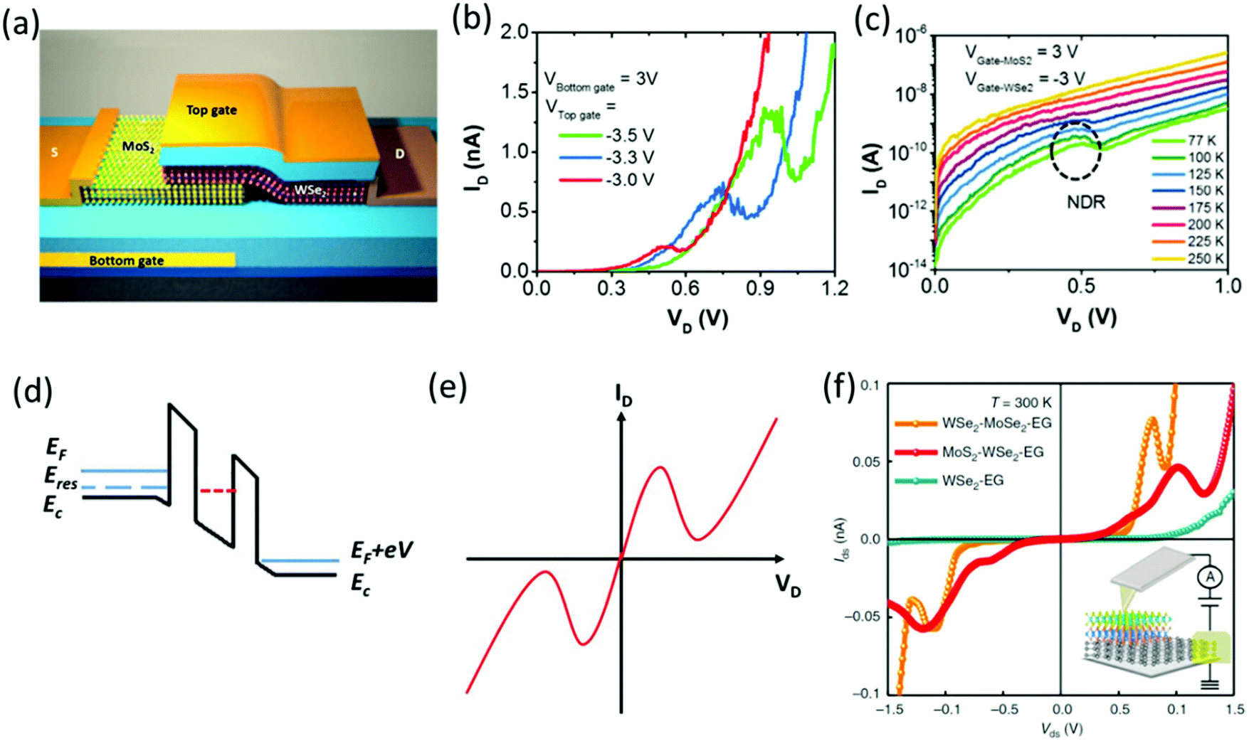 | ||
| Fig. 9 (a) Three-dimensional schematic of an Esaki diode based on a 2D heterojunction of MoS2 and WSe2. (b) ID–VD curves of the Esaki diode in (a). (c) Temperature dependence of the NDR at VGate-MoS2 = −VGate-WSe2 = 3 V. (a–c) Reproduced with permission.153 Copyright 2015, American Chemical Society. (d) Illustration of the energy band diagram of an RTD. (e) Illustration of the I–V curves of an RTD. (d and e) Reproduced with permission.13 Copyright 2019, IOP Publishing. (f) Experimental I–V curves for different combinations of TMDC–graphene interfaces. Reproduced with permission.154 Copyright 2015, Nature Publishing Group. | ||
TMDC based transistors
Traditional three-terminal transistors are usually built on bulk semiconductors such as Si, GaAs, ZnO, etc. Over the past few decades, the dimensions of these materials have been dramatically scaled down below 10 nm following Moore's law and quickly approached the thermal and quantum limits. Atomically thin 2D TMDCs have emerged to gain tremendous attention owing to their potential in creating smaller transistors. As shown in Fig. 10a and b, Desai et al. have experimentally demonstrated ultra-short MoS2 FETs with an ultimate gate length of 1 nm by using a single-walled carbon nanotube (SWCNT) as the gate electrode.155 The bilayer MoS2 transistor exhibits excellent switching performances with high on/off current ratios and a low SS of ∼65 mV per decade (Fig. 10c), which may result from the minimized parasitic gate to source–drain capacitance via introduction of a 1 nm-SWCNT gate. However, there is a thermionic limit of the SS of 60 mV per decade at room temperature for traditional metal–oxide–semiconductor FETs (MOSFETs), precluding further lowering of the overall power consumption. To address this critical issue, negative capacitance FETs (NC-FETs) have been proposed to overcome such a fundamental limit by the use of the intrinsic polarization of ferroelectric (FE) materials to amplify the channel potential, accordingly steepening the SS.156–159 As shown in Fig. 10d and e, Wang et al. recently reported a MoS2 NC-FET by introducing CuInP2S6 (CIPS) as the ferroelectric dielectric and thin h-BN layers for capacitance matching. A sub-60 mV dec−1 SS was achieved for the MoS2 NC-FET and the hysteresis is significantly suppressed by incorporating a 7.5 nm h-BN layer (Fig. 10f). Moreover, by introducing different kinds of dielectrics, advanced functional transistors of TMDCs can be readily designed. Xie et al. demonstrated coplanar-gate electric-double-layer (EDL) MoS2 neuromorphic transistors with proton-conducting poly(vinyl alcohol) electrolytes, successfully mimicking several complementary synaptic functions.160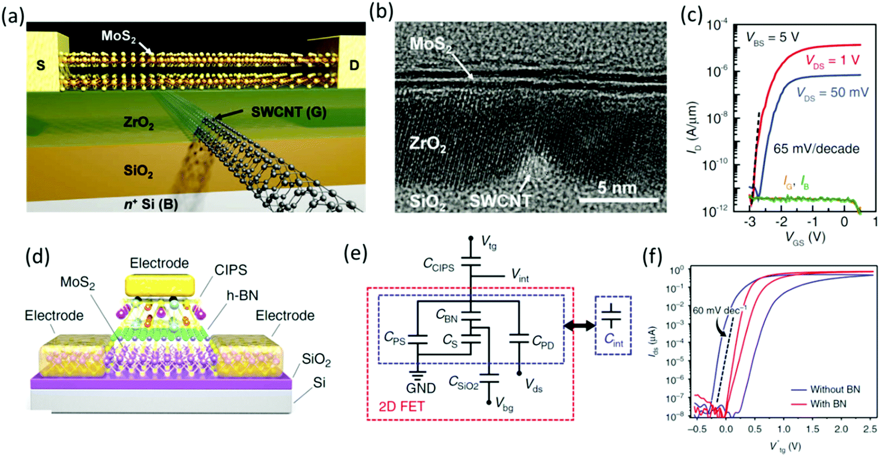 | ||
| Fig. 10 (a) Schematic of the 1 nm-gate MoS2 FET. (b) Cross-sectional TEM image of a bilayer MoS2 FET with a SWCNT gate and ZrO2 gate dielectric. (c) ID–VGS curves of the bilayer MoS2 FET. (d) Schematic diagram of a CIPS/BN/MoS2 vdW NC-FET. (a–c) Reproduced with permission.155 Copyright 2016, AAAS. (e) Equivalent capacitor network of the CIPS/BN/MoS2 vdW NC-FET in (d). (f) Top-gate transfer characteristics of vdW NC-FETs with and without an interfacial h-BN layer. (d–f) Reproduced with permission.157 Copyright 2019, Nature Publishing Group. | ||
TMDC based circuits
Within just a few years, great effort on TMDCs has been devoted to exploring their application in integrated circuits and tremendous progress has been achieved owing to their unprecedented properties. Zhang et al. have demonstrated a one-step synthesis method for fabricating MoTe2 circuits through the phase-patterned growth of ultrathin MoTe2.161 As shown in Fig. 11a, MoTe2 in an inverter configuration can serve as both the transistor channel and metallic component based on its structure of the hexagonal (2H MoTe2) or monoclinic (1T′ MoTe2) phase, respectively. The inverter exhibits excellent logic-level conservation (Fig. 11b) and high voltage gain up to ∼35 (Fig. 11c). Such a strategy of phase engineering allows one to reduce the contact resistances and meanwhile avoids structural damage for ultrathin semiconductors, facilitating the realization of high performance circuits and offering an alternative design architecture. In 2012, Wang et al. demonstrated a NAND, an SRAM and a five-stage ring oscillator based on 2D MoS2 (Fig. 11d–g).162 The ring oscillator constructed by integrating 12 bilayer MoS2 transistors together presents robust oscillation according to the output voltage curves and corresponding frequency power spectrum (Fig. 11f and g), illustrating stable operation in all five inverter stages and showing its great potential for complex integrated circuits. Moving a step forward, in 2017, Wachter et al. experimentally presented a 1-bit implementation of a microprocessor based on 115 MoS2 transistors and the NMOS logic family (Fig. 11h).163 The fabricated microprocessor on CVD synthesized MoS2 is able to deliver the correct result with good signal integrity rail-to-rail performance, demonstrating the feasibility of using a 2D TMDC for realizing a microprocessor.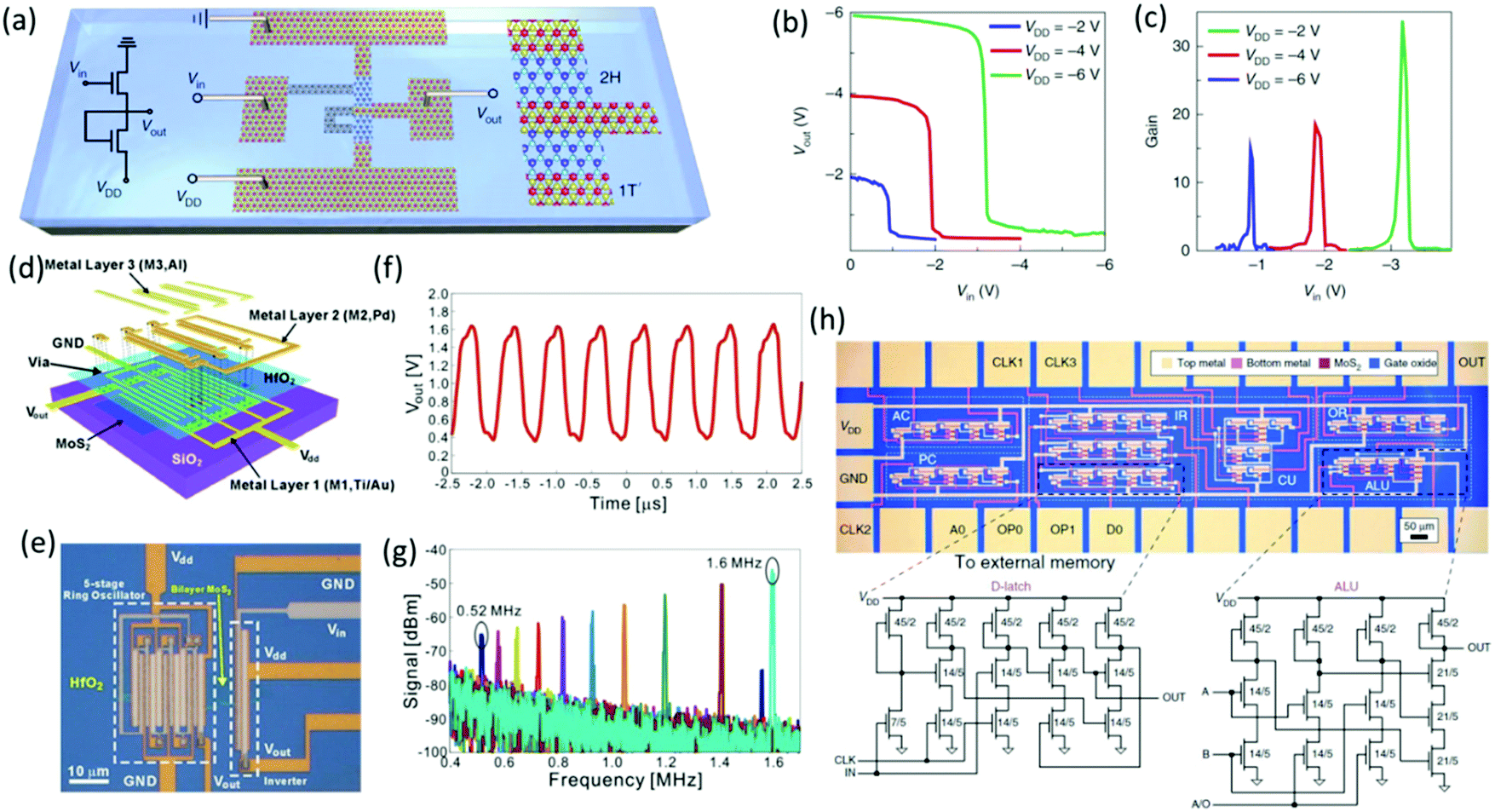 | ||
| Fig. 11 (a) Illustration of a chemically synthesized inverter, where 2H MoTe2 served as the channels and 1T′ MoTe2 as the contacts and interconnects. (b) Typical transfer characteristics of the MoTe2 inverter in (a) operating at different VDD. (c) Signal gains of the MoTe2 inverter. (a–c) Reproduced with permission.161 Copyright 2019, Nature Publishing Group. (d) Schematic illustration of an integrated five-stage ring oscillator circuit on MoS2, consisting of 12 MoS2 FETs. (e) Optical micrograph of the ring oscillator constructed on bilayer MoS2. (f) Output voltage as a function of time for the ring oscillator at Vdd = 2 V. (g) The power spectrum of the output signal as a function of Vdd. (d–g) Reproduced with permission.162 Copyright 2012, American Chemical Society. (h) Microscope image of the MoS2 microprocessor including a D-latch and ALU. Reproduced with permission.163 Copyright 2017, Nature Publishing Group. | ||
TMDC based memories
The development of current computing architectures faces obstacles such as Moore's law, the memory wall and the heat wall (Fig. 12a).164,165 Memristors have been explored for non-volatile RRAM and neuromorphic computing owing to their higher endurance, faster read/write speed and multi-bit storage in comparison with flash memory, driving new computing systems towards on-chip memory and storage, biologically inspired computing and in-memory computing (Fig. 12a). 2D layered TMDCs can help push the forefront of memories beyond the conventional hierarchy, achieving low-power intelligent systems.166–177 Wang et al. reported memristors with a structure of graphene/MoS2−xOx/graphene (GMG) (Fig. 12b),168 where the MoS2−xOx layer is obtained from oxidizing mechanically exfoliated MoS2. The GMG-based memristors show excellent bipolar resistive switching with endurance up to 107, and high thermal stability with an operating temperature of up to 340 °C (Fig. 12c), indicating potential applications in high-temperature harsh electronics. The high performance of the GMG-based memristors is believed to originate from oxidized MoS2−xOx and the atomically sharp interface formed between graphene and MoS2−xOx. Akinwande et al. reported pioneering work of vertical atomristors sandwiching a single TMDC monolayer between two inert Au electrodes, achieving forming-free and stable nonvolatile resistance switching.178,179 Moreover, the MoS2 atomristor is demonstrated to enable switching with low insertion loss and high isolation to 50 GHz, and scalable cutoff frequencies beyond 100 THz.178 Later, Xu et al. developed a MoS2 vertical memristor that sandwiches two MoS2 monolayers between an active Cu electrode and an inert Au electrode.172 In such a MoS2 memristor structure, Cu ions diffuse through the MoS2 layers to form atomic-scale filaments. Low switching voltages down to 0.1–0.2 V are realized owing to the atomic-scale thickness of the active layer and the electrochemical metallization.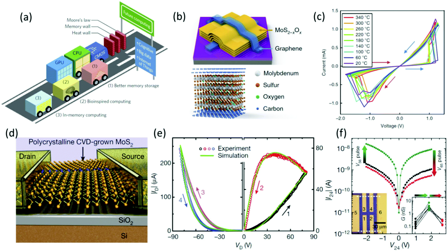 | ||
| Fig. 12 (a) The race towards future computing solutions. Reproduced with permission.164 Copyright 2018, Nature Publishing Group. (b) Top: Schematic diagram of the graphene–MoS2−xOx–graphene (GMG) devices. Bottom: Crystal structure of the GMG devices. (c) DC switching curves of a GMG device with an electroforming current compliance of 1 mA. (b and c) Reproduced with permission.168 Copyright 2018, Nature Publishing Group. (d) Schematic of a MoS2 memtransistor device. (e) ID–VD curve of a MoS2 memtransistor (L = 5 μm, W = 100 μm) at gate bias VG = 10 V. (f) I24–V24 curve between terminals 2 and 4 of a six-terminal MoS2 memtransistor. Reproduced with permission.175 Copyright 2018, Nature Publishing Group. | ||
By integrating various 2D materials, one is able to construct novel memories. Vu et al. demonstrated an array of tunneling random-access memory (TRAM) by using CVD-grown MoS2 as a channel and graphene as a trap layer with ALD-grown Al2O3 as the tunneling barrier, which shows a high on/off ratio and excellent durability.180 In addition, by using a semi-floating gate architecture and band-engineered vdW heterostructures, Liu et al. developed a quasi-non-volatile 2D RAM (where WSe2 works as the channel material, MoS2/h–BN as the semi-blocking layer, HfS2 as the floating gate and a WSe2/MoS2 heterojunction as the p–n junction switch), filling the timescale gap between volatile and non-volatile memory technologies.151 Moreover, Sangwan et al. demonstrated a multi-terminal hybrid memristor and transistor (namely memtransistor) based on polycrystalline monolayer MoS2.175Fig. 12d is the schematic of a MoS2 memtransistor device and Fig. 12e shows the typical ID–VD curve indicating LRS–HRS memtransistors. Besides a high LRS/HRS switching ratio, the 2D MoS2 memtransistor exhibits large gate tunability in individual states by 4 orders of magnitude. Gate-tunable heterosynaptic functionality, which is not achievable in 2-terminal memristors, is also demonstrated in 6-terminal MoS2 memtransistors (Fig. 12f), enabling the realization of complex neural circuits. It is revealed that the resistive switching in the polycrystalline monolayer MoS2 memtransistor is due to the bias-induced motion of MoS2 defects, which dynamically tunes the SHB.
5. Challenges and future prospects
In the past decade, interest in varying 2D layered TMDCs for future nano-electronics is remarkably growing due to their fascinating properties and great progress has been made in TMDCs from synthetic methods and characterization techniques to promising applications. However, the performance of the current 2D TMDCs devices is generally limited by their non-ideal interfaces. In this review, we summarized the recent advances in interface engineering for TMDCs and the novel electronic devices based on diverse TMDCs.Regarding the contact/TMDC interface, it is difficult to obtain ohmic contacts with low contact resistance because of the atomic-scale thickness and pristine surface of TMDCs without deliberately doping. The large surface/volume ratio of atomically thin TMDC also makes the performance of 2D FETs sensitive to interface disorder between the contacts and TMDCs. The traditional contact method gives rise to the formation of gap states and Fermi level pinning, which significantly increases the contact resistance and degrades the device performance. Therefore, new routes of contact and interface engineering must be developed in both theoretical and experimental aspects. Recently, impressive progress towards high quality electrical contacts and high device performance has been identified. However, the contact resistances of TMDCs are still 1–2 orders of magnitude higher than Si CMOS. In this regard, the devices based on 2D TMDCs have plenty more room for lowering the contact resistance and optimizing the performance. For top gated 2D-FETs, due to the absence of contact gating, the contact resistance is usually very large. Therefore, how to obtain low resistance contacts for top gated 2D-FETs is an open question for future electronic devices. In addition, even though some approaches could reduce the contact resistance of TMDCs (such as inserting h-BN as a buffer layer), they are difficult to currently apply for ultra-scaled devices.
Moreover, the implementation of electronic devices like diodes, transistors and circuits based on 2D TMDCs requires controllable channel engineering to further tune the carrier type and density. Conventional doping techniques may not work for ultrathin 2D TMDCs and meanwhile bring additional surface damage, leading to performance degradation. Deliberate defect engineering by ion implantation and plasma treatment would lead to novel physics. Introducing high-k dielectrics and h-BN with a pristine surface may be effective and promising methods to suppress the charge impurity and improve the device performance. Using negative capacitance in TMDC based transistors enables further lowering the SS beyond the thermionic limit. Although surface charge transfer doping has been identified as a non-destructive means for effectively modulating the properties of 2D TMDCs, it is highly desired to address the applicability, efficiency and stability in the future. Addressing both contact and channel engineering for 2D layered TMDCs allows constructing diverse devices to meet the requirements of future electronics.
Conflicts of interest
There are no conflicts to declare.Acknowledgements
The work was partially supported by the financial support from the Science and Technology Development Fund (No. 007/2017/A1 and 132/2017/A3), Macao Special Administration Region (SAR), China, National Natural Science Fund (Grant No. 61904110, 61875138, 61435010, and 6181101252), Natural Science Foundation of Shenzhen University (Grant No. 2019013), and Young Teachers’ Startup Fund for Scientific Research of Shenzhen University (Grant No. 860-000002110426).References
- M. Chhowalla, D. Jena and H. Zhang, Nat. Rev. Mater., 2016, 1, 16052 CrossRef CAS.
- G. Fiori, F. Bonaccorso, G. Iannaccone, T. Palacios, D. Neumaier, A. Seabaugh, S. K. Banerjee and L. Colombo, Nat. Nanotechnol., 2014, 9(10), 768–779 CrossRef CAS PubMed.
- Y. Liu, X. Duan, Y. Huang and X. Duan, Chem. Soc. Rev., 2018, 47(16), 6388–6409 RSC.
- K. S. Novoselov, A. K. Geim, S. V. Morozov, D. Jiang, Y. Zhang, S. V. Dubonos, I. V. Grigorieva and A. A. Firsov, Science, 2004, 306(5696), 666–669 CrossRef CAS PubMed.
- H. Zhang, S. B. Lu, J. Zheng, J. Du, S. C. Wen, D. Y. Tang and K. P. Loh, Opt. Express, 2014, 22(6), 7249–7260 CrossRef CAS PubMed.
- B. Wen, Y. Zhu, D. Yudistira, A. Boes, L. Zhang, T. Yidirim, B. Liu, H. Yan, X. Sun, Y. Zhou, Y. Xue, Y. Zhang, L. Fu, A. Mitchell, H. Zhang and Y. Lu, ACS Nano, 2019, 13, 5335–5343 CrossRef CAS PubMed.
- X. Wang and F. Xia, Nat. Mater., 2015, 14, 264 CrossRef CAS PubMed.
- A. K. Geim, Science, 2009, 324(5934), 1530 CrossRef CAS PubMed.
- D. Akinwande, N. Petrone and J. Hone, Nat. Commun., 2014, 5, 5678 CrossRef CAS PubMed.
- Q. H. Wang, K. Kalantar-Zadeh, A. Kis, J. N. Coleman and M. S. Strano, Nat. Nanotechnol., 2012, 7(11), 699–712 CrossRef CAS.
- J. Pei, J. Yang, T. Yildirim, H. Zhang and Y. Lu, Adv. Mater., 2019, 31(2), e1706945 CrossRef.
- A. Allain, J. Kang, K. Banerjee and A. Kis, Nat. Mater., 2015, 14(12), 1195–1205 CrossRef CAS PubMed.
- W. Zhu, T. Low, H. Wang, P. Ye and X. Duan, 2D Mater., 2019, 6(3), 032004 CrossRef CAS.
- Y. Lv, W. Qin, C. Wang, L. Liao and X. Liu, Adv. Electron. Mater., 2019, 5(1), 1800569 CrossRef.
- X. Jing, Y. Illarionov, E. Yalon, P. Zhou, T. Grasser, Y. Shi and M. Lanza, Adv. Funct. Mater., 2019, 1901971 CrossRef.
- B. Jiang, Z. Yang, X. Liu, Y. Liu and L. Liao, Nano Today, 2019, 25, 122–134 CrossRef CAS.
- D. S. Schulman, A. J. Arnold and S. Das, Chem. Soc. Rev., 2018, 47(9), 3037–3058 RSC.
- Y. Zhao, K. Xu, F. Pan, C. Zhou, F. Zhou and Y. Chai, Adv. Funct. Mater., 2017, 27(19), 1603484 CrossRef.
- G.-S. Kim, S.-H. Kim, J. Park, K. H. Han, J. Kim and H.-Y. Yu, ACS Nano, 2018, 12(6), 6292–6300 CrossRef CAS.
- R. T. Tung, Appl. Phys. Rev., 2014, 1(1), 011304 Search PubMed.
- Y. Wang, J. C. Kim, R. J. Wu, J. Martinez, X. Song, J. Yang, F. Zhao, A. Mkhoyan, H. Y. Jeong and M. Chhowalla, Nature, 2019, 568(7750), 70–74 CrossRef CAS PubMed.
- K. Sotthewes, R. Van Bremen, E. Dollekamp, T. Boulogne, K. Nowakowski, D. Kas, H. J. W. Zandvliet and P. Bampoulis, J. Phys. Chem. C, 2019, 123(9), 5411–5420 CrossRef CAS PubMed.
- R. Addou, L. Colombo and R. M. Wallace, ACS Appl. Mater. Interfaces, 2015, 7(22), 11921–11929 CrossRef CAS.
- S. McDonnell, R. Addou, C. Buie, R. M. Wallace and C. L. Hinkle, ACS Nano, 2014, 8(3), 2880–2888 CrossRef CAS.
- S. Das and J. Appenzeller, Nano Lett., 2013, 13(7), 3396–3402 CrossRef CAS.
- A. Kerelsky, A. Nipane, D. Edelberg, D. Wang, X. Zhou, A. Motmaendadgar, H. Gao, S. Xie, K. Kang, J. Park, J. Teherani and A. Pasupathy, Nano Lett., 2017, 17(10), 5962–5968 CrossRef CAS PubMed.
- S. Das, H.-Y. Chen, A. V. Penumatcha and J. Appenzeller, Nano Lett., 2013, 13(1), 100–105 CrossRef CAS PubMed.
- C. Kim, I. Moon, D. Lee, M. S. Choi, F. Ahmed, S. Nam, Y. Cho, H.-J. Shin, S. Park and W. J. Yoo, ACS Nano, 2017, 11(2), 1588–1596 CrossRef CAS PubMed.
- M. Farmanbar and G. Brocks, Adv. Electron. Mater., 2016, 2(4), 1500405 CrossRef.
- Y. Liu, P. Stradins and S.-H. Wei, Sci. Adv., 2016, 2(4), e1600069 CrossRef PubMed.
- C. D. English, G. Shine, V. E. Dorgan, K. C. Saraswat and E. Pop, Nano Lett., 2016, 16(6), 3824–3830 CrossRef CAS PubMed.
- A. Dankert, L. Langouche, M. V. Kamalakar and S. P. Dash, ACS Nano, 2014, 8(1), 476–482 CrossRef CAS.
- J.-R. Chen, P. M. Odenthal, A. G. Swartz, G. C. Floyd, H. Wen, K. Y. Luo and R. K. Kawakami, Nano Lett., 2013, 13(7), 3106–3110 CrossRef CAS.
- S. Lee, A. Tang, S. Aloni and H. S. Philip Wong, Nano Lett., 2016, 16(1), 276–281 CrossRef CAS.
- Y. Liu, H. Wu, H.-C. Cheng, S. Yang, E. Zhu, Q. He, M. Ding, D. Li, J. Guo, N. O. Weiss, Y. Huang and X. Duan, Nano Lett., 2015, 15(5), 3030–3034 CrossRef CAS PubMed.
- L. Yu, Y.-H. Lee, X. Ling, E. J. G. Santos, Y. C. Shin, Y. Lin, M. Dubey, E. Kaxiras, J. Kong, H. Wang and T. Palacios, Nano Lett., 2014, 14(6), 3055–3063 CrossRef CAS PubMed.
- Y. T. Lee, K. Choi, H. S. Lee, S.-W. Min, P. J. Jeon, D. K. Hwang, H. J. Choi and S. Im, Small, 2014, 10(12), 2356–2361 CrossRef CAS.
- W. Hong, G. W. Shim, S. Y. Yang, D. Y. Jung and S. Y. Choi, Adv. Funct. Mater., 2019, 29(6), 1807550 CrossRef.
- R. Maiti, S. Haldar, D. Majumdar, A. Singha and S. K. Ray, Nanotechnology, 2017, 28(7), 075707 CrossRef CAS PubMed.
- C. Gong, D. Hinojos, W. Wang, N. Nijem, B. Shan, R. M. Wallace, K. Cho and Y. J. Chabal, ACS Nano, 2012, 6(6), 5381–5387 CrossRef CAS PubMed.
- S.-S. Chee, D. Seo, H. Kim, H. Jang, S. Lee, S. P. Moon, K. H. Lee, S. W. Kim, H. Choi and M.-H. Ham, Adv. Mater., 2019, 31(2), 1804422 CrossRef PubMed.
- J. Wang, Q. Yao, C. W. Huang, X. Zou, L. Liao, S. Chen, Z. Fan, K. Zhang, W. Wu, X. Xiao, C. Jiang and W. W. Wu, Adv. Mater., 2016, 28, 8302–8308 CrossRef CAS PubMed.
- X. Cui, E.-M. Shih, L. A. Jauregui, S. H. Chae, Y. D. Kim, B. Li, D. Seo, K. Pistunova, J. Yin, J.-H. Park, H.-J. Choi, Y. H. Lee, K. Watanabe, T. Taniguchi, P. Kim, C. R. Dean and J. C. Hone, Nano Lett., 2017, 17(8), 4781–4786 CrossRef CAS.
- X. Cui, G. H. Lee, Y. D. Kim, G. Arefe, P. Y. Huang, C. H. Lee, D. A. Chenet, X. Zhang, L. Wang, F. Ye, F. Pizzocchero, B. S. Jessen, K. Watanabe, T. Taniguchi, D. A. Muller, T. Low, P. Kim and J. Hone, Nat. Nanotechnol., 2015, 10(6), 534–540 CrossRef CAS.
- J. H. Kang, W. Liu, D. Sarkar, D. Jena and K. Banerjee, Phys. Rev. X, 2014, 4(3), 031005 Search PubMed.
- L. Wang, I. Meric, P. Y. Huang, Q. Gao, Y. Gao, H. Tran, T. Taniguchi, K. Watanabe, L. M. Campos, D. A. Muller, J. Guo, P. Kim, J. Hone, K. L. Shepard and C. R. Dean, Science, 2013, 342(6158), 614 CrossRef CAS.
- B. H. Moon, G. H. Han, H. Kim, H. Choi, J. J. Bae, J. Kim, Y. Jin, H. Y. Jeong, M.-K. Joo, Y. H. Lee and S. C. Lim, ACS Appl. Mater. Interfaces, 2017, 9(12), 11240–11246 CrossRef CAS.
- Z. Yang, C. Kim, K. Y. Lee, M. Lee, S. Appalakondaiah, C.-H. Ra, K. Watanabe, T. Taniguchi, K. Cho, E. Hwang, J. Hone and W. J. Yoo, Adv. Mater., 2019, 31, 25 Search PubMed.
- M. H. D. Guimaraes, H. Gao, Y. Han, K. Kang, S. Xie, C.-J. Kim, D. A. Muller, D. C. Ralph and J. Park, ACS Nano, 2016, 10(6), 6392–6399 CrossRef CAS PubMed.
- A. Allain, J. H. Kang, K. Banerjee and A. Kis, Nat. Mater., 2015, 14(12), 1195–1205 CrossRef CAS.
- X. Ling, Y. Lin, Q. Ma, Z. Wang, Y. Song, L. Yu, S. Huang, W. Fang, X. Zhang, A. L. Hsu, Y. Bie, Y.-H. Lee, Y. Zhu, L. Wu, J. Li, P. Jarillo-Herrero, M. Dresselhaus, T. Palacios and J. Kong, Adv. Mater., 2016, 28(12), 2322–2329 CrossRef CAS.
- C. H. Chu, H. C. Lin, C. H. Yeh, Z. Y. Liang, M. Y. Chou and P. W. Chiu, ACS Nano, 2019, 13(7), 8146–8154 CrossRef CAS.
- H. Fang, S. Chuang, T. C. Chang, K. Takei, T. Takahashi and A. Javey, Nano Lett., 2012, 12(7), 3788–3792 CrossRef CAS.
- H.-J. Chuang, B. Chamlagain, M. Koehler, M. M. Perera, J. Yan, D. Mandrus, D. Tomanek and Z. Zhou, Nano Lett., 2016, 16(3), 1896–1902 CrossRef CAS PubMed.
- S.-Y. Seo, J. Park, J. Park, K. Song, S. Cha, S. Sim, S.-Y. Choi, H. W. Yeom, H. Choi and M.-H. J. N. E. Jo, Nat. Electron., 2018, 1(9), 512 CrossRef CAS.
- R. Pisoni, A. Kormanyos, M. Brooks, Z. Lei, P. Back, M. Eich, H. Overweg, Y. Lee, P. Rickhaus, K. Watanabe, T. Taniguchi, A. Imamoglu, G. Burkard, T. Ihn and K. Ensslin, Phys. Rev. Lett., 2018, 121(24), 247701 CrossRef CAS PubMed.
- B. Fallahazad, H. C. P. Movva, K. Kim, S. Larentis, T. Taniguchi, K. Watanabe, S. K. Banerjee and E. Tutuc, Phys. Rev. Lett., 2016, 116(8), 086601 CrossRef PubMed.
- H. C. P. Movva, A. Rai, S. Kang, K. Kim, B. Fallahazad, T. Taniguchi, K. Watanabe, E. Tutuc and S. K. Banerjee, ACS Nano, 2015, 9(10), 10402–10410 CrossRef CAS PubMed.
- Y. Wang, J. Xiao, H. Zhu, Y. Li, Y. Alsaid, K. Y. Fong, Y. Zhou, S. Wang, W. Shi, Y. Wang, A. Zettl, E. J. Reed and X. Zhang, Nature, 2017, 550(7677), 487–491 CrossRef CAS PubMed.
- S. Cho, S. Kim, J. H. Kim, J. Zhao, J. Seok, D. H. Keum, J. Baik, D.-H. Choe, K. J. Chang, K. Suenaga, S. W. Kim, Y. H. Lee and H. Yang, Science, 2015, 349(6248), 625–628 CrossRef CAS PubMed.
- S. Song, D. H. Keum, S. Cho, D. Perello, Y. Kim and Y. H. Lee, Nano Lett., 2016, 16(1), 188–193 CrossRef CAS PubMed.
- R. Kappera, D. Voiry, S. E. Yalcin, B. Branch, G. Gupta, A. D. Mohite and M. Chhowalla, Nat. Mater., 2014, 13(12), 1128–1134 CrossRef CAS PubMed.
- J. Q. Zhu, Z. C. Wang, H. Yu, N. Li, J. Zhang, J. L. Meng, M. Z. Liao, J. Zhao, X. B. Lu, L. J. Du, R. Yang, D. Shi, Y. Jiang and G. Y. Zhang, J. Am. Chem. Soc., 2017, 139(30), 10216–10219 CrossRef CAS PubMed.
- Y. Zhao, J. Qiao, Z. Yu, P. Yu, K. Xu, S. P. Lau, W. Zhou, Z. Liu, X. Wang and W. Ji, Adv. Mater., 2017, 29(5), 1604230 CrossRef.
- Y. Zhao, J. Qiao, P. Yu, Z. Hu, Z. Lin, S. P. Lau, Z. Liu, W. Ji and Y. Chai, Adv. Mater., 2016, 28(12), 2399–2407 CrossRef CAS.
- C.-S. Lee, S. J. Oh, H. Heo, S.-Y. Seo, J. Kim, Y. H. Kim, D. Kim, O. F. N. Okello, H. Shin, J. H. Sung, S.-Y. Choi, J. S. Kim, J. K. Kim and M.-H. Jo, Nano Lett., 2019, 19(3), 1814–1820 CrossRef CAS.
- W. S. Leong, Q. Ji, N. Mao, Y. Han, H. Wang, A. J. Goodman, A. Vignon, C. Su, Y. Guo, P.-C. Shen, Z. Gao, D. A. Muller, W. A. Tisdale and J. Kong, J. Am. Chem. Soc., 2018, 140(39), 12354–12358 CrossRef CAS.
- J. H. Sung, H. Heo, S. Si, Y. H. Kim, H. R. Noh, K. Song, J. Kim, C.-S. Lee, S.-Y. Seo, D.-H. Kim, H. K. Kim, H. W. Yeom, T.-H. Kim, S.-Y. Choi, J. S. Kim and M.-H. Jo, Nat. Nanotechnol., 2017, 12(11), 1064 CrossRef CAS.
- X. Zhang, Z. Jin, L. Wang, J. A. Hachtel, E. Villarreal, Z. Wang, T. Ha, Y. Nakanishi, C. S. Tiwary, J. Lai, L. Dong, J. Yang, R. Vajtai, E. Ringe, J. C. Idrobo, B. I. Yakobson, J. Lou, V. Gambin, R. Koltun and P. M. Ajayan, ACS Appl. Mater. Interfaces, 2019, 11(13), 12777–12785 CrossRef CAS.
- Y. Liu, J. Guo, E. Zhu, L. Liao, S.-J. Lee, M. Ding, I. Shakir, V. Gambin, Y. Huang and X. Duan, Nature, 2018, 557(7707), 696–700 CrossRef CAS PubMed.
- S. M. Sze and K. K. Ng, Physics of semiconductor devices, John Wiley & Sons, 2006 Search PubMed.
- W. A. Saidi, J. Chem. Phys., 2014, 141(9), 094707 CrossRef PubMed.
- Y. Jung, M. S. Choi, A. Nipane, A. Borah, B. Kim, A. Zangiabadi, T. Taniguchi, K. Watanabe, W. J. Yoo and J. J. N. E. Hone, Nat. Electron., 2019, 2(5), 187–194 CrossRef.
- W. Liao, W. Wei, Y. Tong, W. K. Chim and C. Zhu, Appl. Phys. Lett., 2017, 111(8), 082105 CrossRef.
- F. Gao, H. Yang and P. Hu, Small Methods, 2018, 2(6), 1700384 CrossRef.
- Y. Jeong, J. H. Park, J. Ahn, J. Y. Lim, E. Kim and S. Im, Adv. Mater. Interfaces, 2018, 5(19), 1800812 CrossRef.
- B. Cheng, M. Cao, R. Rao, A. Inani, P. V. Voorde, W. M. Greene, J. M. C. Stork, Y. Zhiping, P. M. Zeitzoff and J. C. S. Woo, IEEE Trans. Electron Devices, 1999, 46(7), 1537–1544 CrossRef CAS.
- D. Jena and A. Konar, Phys. Rev. Lett., 2007, 98(13), 136805 CrossRef PubMed.
- B. Wang, W. Huang, L. Chi, M. Al-Hashimi, T. J. Marks and A. Facchetti, Chem. Rev., 2018, 118(11), 5690–5754 CrossRef CAS PubMed.
- B. Radisavljevic and A. Kis, Nat. Mater., 2013, 12(9), 815–820 CrossRef CAS PubMed.
- B. Radisavljevic, A. Radenovic, J. Brivio, I. V. Giacometti and A. Kis, Nat. Nanotechnol., 2011, 6(3), 147–150 CrossRef CAS PubMed.
- K. K. Kim, H. S. Lee and Y. H. Lee, Chem. Soc. Rev., 2018, 47(16), 6342–6369 RSC.
- W. Liao, Y. Huang, H. Wang and H. Zhang, Appl. Mater. Today, 2019, 16, 435–455 CrossRef.
- M. Yankowitz, Q. Ma, P. Jarillo-Herrero and B. J. LeRoy, Nat. Rev. Phys., 2019, 1(2), 112–125 CrossRef.
- J. Shim, D.-H. Kang, Y. Kim, H. Kum, W. Kong, S.-H. Bae, I. Almansouri, K. Lee, J.-H. Park and J. Kim, Carbon, 2018, 133, 78–89 CrossRef CAS.
- M. W. Iqbal, M. Z. Iqbal, M. F. Khan, M. A. Shehzad, Y. Seo, J. H. Park, C. Hwang and J. Eom, Sci. Rep., 2015, 5, 10699 CrossRef CAS PubMed.
- M. Y. Chan, K. Komatsu, S.-L. Li, Y. Xu, P. Darmawan, H. Kuramochi, S. Nakaharai, A. Aparecido-Ferreira, K. Watanabe, T. Taniguchi and K. Tsukagoshi, Nanoscale, 2013, 5(20), 9572–9576 RSC.
- Y. Y. Illarionov, A. G. Banshchikov, D. K. Polyushkin, S. Wachter, T. Knobloch, M. Thesberg, L. Mennel, M. Paur, M. Stöger-Pollach, A. Steiger-Thirsfeld, M. I. Vexler, M. Waltl, N. S. Sokolov, T. Mueller and T. Grasser, Nat. Electron., 2019, 2(6), 230–235 CrossRef CAS.
- A. Li, Q. Chen, P. Wang, Y. Gan, T. Qi, P. Wang, F. Tang, J. Z. Wu, R. Chen, L. Zhang and Y. Gong, Adv. Mater., 2019, 31(6), e1805656 CrossRef PubMed.
- W. Bao, X. Cai, D. Kim, K. Sridhara and M. S. Fuhrer, Appl. Phys. Lett., 2013, 102(4), 042104 CrossRef.
- W. Feng, W. Zheng, W. Cao and P. Hu, Adv. Mater., 2014, 26(38), 6587–6593 CrossRef CAS PubMed.
- X. Wang, J. B. Xu, C. Wang, J. Du and W. Xie, Adv. Mater., 2011, 23(21), 2464–2468 CrossRef CAS PubMed.
- T. Kawanago and S. Oda, Appl. Phys. Lett., 2016, 108(4), 041605 CrossRef.
- S. C. Yang, J. Choi, B. C. Jang, W. Hong, G. W. Shim, S. Y. Yang, S. G. Im and S. Y. Choi, Adv. Electron. Mater., 2019, 5(5), 1800688 CrossRef.
- B. Chamlagain, Q. Cui, S. Paudel, M. M.-C. Cheng, P.-Y. Chen and Z. Zhou, 2D Mater., 2017, 4(3), 031002 CrossRef.
- M. Si, C.-J. Su, C. Jiang, N. J. Conrad, H. Zhou, K. D. Maize, G. Qiu, C.-T. Wu, A. Shakouri and M. A. Alam, Nat. Nanotechnol., 2018, 13(1), 24 CrossRef CAS PubMed.
- X. Liu, R. Liang, G. Gao, C. Pan, C. Jiang, Q. Xu, J. Luo, X. Zou, Z. Yang, L. Liao and Z. L. Wang, Adv. Mater., 2018, 30(28), 1800932 CrossRef PubMed.
- X. Wang, P. Wang, J. Wang, W. Hu, X. Zhou, N. Guo, H. Huang, S. Sun, H. Shen, T. Lin, M. Tang, L. Liao, A. Jiang, J. Sun, X. Meng, X. Chen, W. Lu and J. Chu, Adv. Mater., 2015, 27(42), 6575–6581 CrossRef CAS.
- Y. Tan, X. Liu, Z. He, Y. Liu, M. Zhao, H. Zhang and F. Chen, ACS Photonics, 2017, 4(6), 1531–1538 CrossRef CAS.
- A. Chang, C. Zhang, Y. Yu, Y. Yu and B. Zhang, ACS Appl. Mater. Interfaces, 2018, 10(49), 41861–41865 CrossRef CAS PubMed.
- Z. Li and F. Chen, Appl. Phys. Rev., 2017, 4(1), 011103 Search PubMed.
- A. Sharma, B. Wen, B. Liu, Y. W. Myint, H. Zhang and Y. Lu, Small, 2018, 14(16), 1704556 CrossRef.
- S. Zheng, Y. Zeng and Z. Chen, IEEE Access, 2019, 7, 79989–79996 Search PubMed.
- D. Wang, Y. Wang, X. Chen, Y. Zhu, K. Zhan, H. Cheng and X. Wang, Nanoscale, 2016, 8(7), 4107–4112 RSC.
- W. Li, X. Zhan, X. Song, S. Si, R. Chen, J. Liu, Z. Wang, J. He and X. Xiao, Small, 2019, 15(31), 1901820 CrossRef.
- H. Guo, Y. Sun, P. Zhai, H. Yao, J. Zeng, S. Zhang, J. Duan, M. Hou, M. Khan and J. Liu, Appl. Phys. A: Mater. Sci. Process., 2016, 122(4), 375 CrossRef.
- S. Jiang, R. Cheng, R. Ng, Y. Huang and X. Duan, Nano Res., 2015, 8(1), 257–262 CrossRef CAS.
- V. Iberi, L. Liang, A. V. Ievlev, M. G. Stanford, M.-W. Lin, X. Li, M. Mahjouri-Samani, S. Jesse, B. G. Sumpter, S. V. Kalinin, D. C. Joy, K. Xiao, A. Belianinov and O. S. Ovchinnikova, Sci. Rep., 2016, 6, 30481 CrossRef CAS PubMed.
- D. S. Fox, Y. Zhou, P. Maguire, A. O’Neill, C. Ó’Coileáin, R. Gatensby, A. M. Glushenkov, T. Tao, G. S. Duesberg, I. V. Shvets, M. Abid, M. Abid, H.-C. Wu, Y. Chen, J. N. Coleman, J. F. Donegan and H. Zhang, Nano Lett., 2015, 15(8), 5307–5313 CrossRef CAS.
- S. Bertolazzi, S. Bonacchi, G. Nan, A. Pershin, D. Beljonne and P. Samorì, Adv. Mater., 2017, 29(18), 1606760 CrossRef PubMed.
- Y. Liu, Z. Gao, Y. Tan and F. Chen, ACS Nano, 2018, 12(10), 10529–10536 CrossRef CAS PubMed.
- Z. Cheng, H. Abuzaid, Y. Yu, F. Zhang, Y. Li, S. G. Noyce, N. X. Williams, Y.-C. Lin, J. L. Doherty, C. Tao, L. Cao and A. D. Franklin, 2D Mater., 2019, 6(3), 034005 CrossRef CAS.
- M. G. Stanford, P. R. Pudasaini, A. Belianinov, N. Cross, J. H. Noh, M. R. Koehler, D. G. Mandrus, G. Duscher, A. J. Rondinone, I. N. Ivanov, T. Z. Ward and P. D. Rack, Sci. Rep., 2016, 6, 27276 CrossRef CAS PubMed.
- Y. Gong, H. Yuan, C.-L. Wu, P. Tang, S.-Z. Yang, A. Yang, G. Li, B. Liu, J. van de Groep, M. L. Brongersma, M. F. Chisholm, S.-C. Zhang, W. Zhou and Y. Cui, Nat. Nanotechnol., 2018, 13(4), 294–299 CrossRef CAS PubMed.
- Z. J. Han, A. T. Murdock, D. H. Seo and A. Bendavid, 2D Mater., 2018, 5(3), 032002 CrossRef.
- J. Jadwiszczak, G. Li, C. P. Cullen, J. J. Wang, P. Maguire, G. S. Duesberg, J. G. Lunney and H. Zhang, Appl. Phys. Lett., 2019, 114(9), 091103 CrossRef.
- T. Lin, B. Kang, M. Jeon, C. Huffman, J. Jeon, S. Lee, W. Han, J. Lee, S. Lee, G. Yeom and K. Kim, ACS Appl. Mater. Interfaces, 2015, 7(29), 15892–15897 CrossRef CAS PubMed.
- Y. Liu, H. Nan, X. Wu, W. Pan, W. Wang, J. Bai, W. Zhao, L. Sun, X. Wang and Z. Ni, ACS Nano, 2013, 7(5), 4202–4209 CrossRef CAS PubMed.
- J. Shim, A. Oh, D.-H. Kang, S. Oh, S. K. Jang, J. Jeon, M. H. Jeon, M. Kim, C. Choi, J. Lee, S. Lee, G. Y. Yeom, Y. J. Song and J.-H. Park, Adv. Mater., 2016, 28(32), 6985–6992 CrossRef CAS PubMed.
- X. Chen, Y. J. Park, T. Das, H. Jang, J.-B. Lee and J.-H. Ahn, Nanoscale, 2016, 8(33), 15181–15188 RSC.
- S. Wi, H. Kim, M. Chen, H. Nam, L. J. Guo, E. Meyhofer and X. Liang, ACS Nano, 2014, 8(5), 5270–5281 CrossRef CAS PubMed.
- P. K. Chow, R. B. Jacobs-Gedrim, J. Gao, T.-M. Lu, B. Yu, H. Terrones and N. Koratkar, ACS Nano, 2015, 9(2), 1520–1527 CrossRef CAS PubMed.
- M. Chen, H. Nam, S. Wi, G. Priessnitz, I. M. Gunawan and X. Liang, ACS Nano, 2014, 8(4), 4023–4032 CrossRef CAS PubMed.
- M. Chen, H. Nam, S. Wi, L. Ji, X. Ren, L. Bian, S. Lu and X. Liang, Appl. Phys. Lett., 2013, 103(14), 142110 CrossRef.
- J. Jadwiszczak, C. O’Callaghan, Y. Zhou, D. S. Fox, E. Weitz, D. Keane, C. P. Cullen, I. O’Reilly, C. Downing, A. Shmeliov, P. Maguire, J. J. Gough, C. McGuinness, M. S. Ferreira, A. L. Bradley, J. J. Boland, G. S. Duesberg, V. Nicolosi and H. Zhang, Sci. Adv., 2018, 4(3), eaao5031 CrossRef PubMed.
- Y. Cho, J. H. Park, M. Kim, Y. Jeong, J. Ahn, T. Kim, H. Choi, Y. Yi and S. Im, Adv. Funct. Mater., 2018, 28(39), 1801204 CrossRef.
- S. Lai, S. Byeon, S. K. Jang, J. Lee, B. H. Lee, J.-H. Park, Y.-H. Kim and S. Lee, Nanoscale, 2018, 10(39), 18758–18766 RSC.
- N. Choudhary, M. R. Islam, N. Kang, L. Tetard, Y. Jung and S. I. Khondaker, J. Phys.: Condens. Matter, 2016, 28(36), 364002 CrossRef PubMed.
- A. N. Hoffman, M. G. Stanford, M. G. Sales, C. Zhang, I. N. Ivanov, S. J. McDonnell, D. G. Mandrus and P. D. Rack, 2D Mater., 2019, 6(4), 045024 CrossRef CAS.
- S. Mouri, Y. Miyauchi and K. Matsuda, Nano Lett., 2013, 13(12), 5944–5948 CrossRef CAS PubMed.
- W. Liao, L. Wang, L. Chen, W. Wei, Z. Zeng, X. Feng, L. Huang, W. C. Tan, X. Huang, K. W. Ang and C. Zhu, Nanoscale, 2018, 10(36), 17007–17014 RSC.
- Z. Guo, S. Chen, Z. Wang, Z. Yang, F. Liu, Y. Xu, J. Wang, Y. Yi, H. Zhang, L. Liao, P. K. Chu and X.-F. Yu, Adv. Mater., 2017, 29(42), 1703811 CrossRef PubMed.
- H.-Y. Park, S. R. Dugasani, D.-H. Kang, J. Jeon, S. K. Jang, S. Lee, Y. Roh, S. H. Park and J.-H. Park, ACS Nano, 2014, 8(11), 11603–11613 CrossRef CAS PubMed.
- S. Tongay, J. Zhou, C. Ataca, J. Liu, J. S. Kang, T. S. Matthews, L. You, J. Li, J. C. Grossman and J. Wu, Nano Lett., 2013, 13(6), 2831–2836 CrossRef CAS PubMed.
- D. Kiriya, M. Tosun, P. Zhao, J. S. Kang and A. Javey, J. Am. Chem. Soc., 2014, 136(22), 7853–7856 CrossRef CAS PubMed.
- Y. Du, H. Liu, A. T. Neal, M. Si and P. D. Ye, IEEE Electron Device Lett., 2013, 34(10), 1328–1330 CAS.
- J. Lin, J. Zhong, S. Zhong, H. Li, H. Zhang and W. Chen, Appl. Phys. Lett., 2013, 103(6), 063109 CrossRef.
- J. D. Lin, C. Han, F. Wang, R. Wang, D. Xiang, S. Qin, X.-A. Zhang, L. Wang, H. Zhang, A. T. S. Wee and W. Chen, ACS Nano, 2014, 8(5), 5323–5329 CrossRef CAS PubMed.
- A. Rai, A. Valsaraj, H. C. P. Movva, A. Roy, R. Ghosh, S. Sonde, S. Kang, J. Chang, T. Trivedi, R. Dey, S. Guchhait, S. Larentis, L. F. Register, E. Tutuc and S. K. Banerjee, Nano Lett., 2015, 15(7), 4329–4336 CrossRef CAS PubMed.
- C. Zhou, Y. Zhao, S. Raju, Y. Wang, Z. Lin, M. Chan and Y. Chai, Adv. Funct. Mater., 2016, 26(23), 4223–4230 CrossRef CAS.
- M. Li, C.-Y. Lin, S.-H. Yang, Y.-M. Chang, J.-K. Chang, F.-S. Yang, C. Zhong, W.-B. Jian, C.-H. Lien, C.-H. Ho, H.-J. Liu, R. Huang, W. Li, Y.-F. Lin and J. Chu, Adv. Mater., 2018, 30(44), 1803690 CrossRef PubMed.
- J. Y. Lim, A. Pezeshki, S. Oh, J. S. Kim, Y. T. Lee, S. Yu, D. K. Hwang, G. H. Lee, H. J. Choi and S. Im, Adv. Mater., 2017, 29(30), 1701798 CrossRef PubMed.
- M. S. Choi, D. Qu, D. Lee, X. Liu, K. Watanabe, T. Taniguchi and W. J. Yoo, ACS Nano, 2014, 8(9), 9332–9340 CrossRef CAS PubMed.
- X. Liu, D. Qu, J. Ryu, F. Ahmed, Z. Yang, D. Lee and W. J. Yoo, Adv. Mater., 2016, 28(12), 2345–2351 CrossRef CAS PubMed.
- D. M. Sim, M. Kim, S. Yim, M.-J. Choi, J. Choi, S. Yoo and Y. S. Jung, ACS Nano, 2015, 9(12), 12115–12123 CrossRef CAS PubMed.
- S.-W. Min, M. Yoon, S. J. Yang, K. R. Ko and S. Im, ACS Appl. Mater. Interfaces, 2018, 10(4), 4206–4212 CrossRef CAS PubMed.
- D. Li, M. Chen, Z. Sun, P. Yu, Z. Liu, P. M. Ajayan and Z. Zhang, Nat. Nanotechnol., 2017, 12, 901–906 CrossRef CAS PubMed.
- P. V. Nguyen, N. C. Teutsch, N. P. Wilson, J. Kahn, X. Xia, A. J. Graham, V. Kandyba, A. Giampietri, A. Barinov, G. C. Constantinescu, N. Yeung, N. D. M. Hine, X. Xu, D. H. Cobden and N. R. Wilson, Nature, 2019, 572(7768), 220–223 CrossRef CAS PubMed.
- X. Zheng, Y. Wei, J. Liu, S. Wang, J. Shi, H. Yang, G. Peng, C. Deng, W. Luo, Y. Zhao, Y. Li, K. Sun, W. Wan, H. Xie, Y. Gao, X. Zhang and H. Huang, Nanoscale, 2019, 11(28), 13469–13476 RSC.
- P. Paletti, R. Yue, C. Hinkle, S. K. Fullerton-Shirey and A. Seabaugh, npj 2D Mater. Appl., 2019, 3(1), 1–7 CrossRef CAS.
- S. Fan, W. Shen, C. An, Z. Sun, S. Wu, L. Xu, D. Sun, X. Hu, D. Zhang and J. Liu, ACS Appl. Mater. Interfaces, 2018, 10(31), 26533–26538 CrossRef CAS PubMed.
- J. W. Chen, S. T. Lo, S. C. Ho, S. S. Wong, T. H. Vu, X. Q. Zhang, Y. D. Liu, Y. Y. Chiou, Y. X. Chen, J. C. Yang, Y. C. Chen, Y. H. Chu, Y. H. Lee, C. J. Chung, T. M. Chen, C. H. Chen and C. L. Wu, Nat. Commun., 2018, 9(1), 3143 CrossRef PubMed.
- T. Roy, M. Tosun, X. Cao, H. Fang, D.-H. Lien, P. Zhao, Y.-Z. Chen, Y.-L. Chueh, J. Guo and A. Javey, ACS Nano, 2015, 9(2), 2071–2079 CrossRef CAS PubMed.
- Y. C. Lin, R. K. Ghosh, R. Addou, N. Lu, S. M. Eichfeld, H. Zhu, M. Y. Li, X. Peng, M. J. Kim, L. J. Li, R. M. Wallace, S. Datta and J. A. Robinson, Nat. Commun., 2015, 6, 7311 CrossRef CAS PubMed.
- S. B. Desai, S. R. Madhvapathy, A. B. Sachid, J. P. Llinas, Q. Wang, G. H. Ahn, G. Pitner, M. J. Kim, J. Bokor and C. Hu, Science, 2016, 354(6308), 99–102 CrossRef CAS PubMed.
- N. Zagni, P. Pavan and M. A. Alam, Appl. Phys. Lett., 2019, 114(23), 233102 CrossRef.
- X. Wang, P. Yu, Z. Lei, C. Zhu, X. Cao, F. Liu, L. You, Q. Zeng, Y. Deng, C. Zhu, J. Zhou, Q. Fu, J. Wang, Y. Huang and Z. Liu, Nat. Commun., 2019, 10(1), 3037 CrossRef PubMed.
- J. Íñiguez, P. Zubko, I. Luk’yanchuk and A. Cano, Nat. Rev. Mater., 2019, 4(4), 243–256 Search PubMed.
- H. Agarwal, P. Kushwaha, Y. Lin, M. Kao, Y. Liao, A. Dasgupta, S. Salahuddin and C. Hu, IEEE Electron Device Lett., 2019, 40(3), 463–466 CAS.
- D. Xie, W. Hu and J. Jiang, Org. Electron., 2018, 63, 120–128 CrossRef CAS.
- Q. Zhang, X.-F. Wang, S.-H. Shen, Q. Lu, X. Liu, H. Li, J. Zheng, C.-P. Yu, X. Zhong, L. Gu, T.-L. Ren and L. Jiao, Nat. Electron., 2019, 2(4), 164–170 CrossRef.
- H. Wang, L. Yu, Y. H. Lee, Y. Shi, A. Hsu, M. L. Chin, L. J. Li, M. Dubey, J. Kong and T. Palacios, Nano Lett., 2012, 12(9), 4674–4680 CrossRef CAS PubMed.
- S. Wachter, D. K. Polyushkin, O. Bethge and T. Mueller, Nat. Commun., 2017, 8, 14948 CrossRef CAS PubMed.
- M. A. Zidan, J. P. Strachan and W. D. Lu, Nat. Electron., 2018, 1(1), 22–29 CrossRef.
- D. Ielmini and H. S. P. Wong, Nat. Electron., 2018, 1(6), 333–343 CrossRef.
- C. Liu, X. Yan, X. Song, S. Ding, D. W. Zhang and P. Zhou, Nat. Nanotechnol., 2018, 13, 404–410 CrossRef CAS PubMed.
- J. Li, L. Liu, X. Chen, C. Liu, J. Wang, W. Hu, D. W. Zhang and P. Zhou, Adv. Mater., 2019, 31(11), e1808035 CrossRef PubMed.
- M. Wang, S. Cai, C. Pan, C. Wang, X. Lian, Y. Zhuo, K. Xu, T. Cao, X. Pan, B. Wang, S.-J. Liang, J. J. Yang, P. Wang and F. Miao, Nat. Electron., 2018, 1(2), 130–136 CrossRef CAS.
- M. Huang, S. Li, Z. Zhang, X. Xiong, X. Li and Y. Wu, Nat. Nanotechnol., 2017, 12(12), 1148–1154 CrossRef CAS PubMed.
- A. A. Bessonov, M. N. Kirikova, D. I. Petukhov, M. Allen, T. Ryhanen and M. J. Bailey, Nat. Mater., 2015, 14(2), 199–204 CrossRef CAS PubMed.
- S. Bertolazzi, D. Krasnozhon and A. Kis, ACS Nano, 2013, 7(4), 3246–3252 CrossRef CAS PubMed.
- R. Xu, H. Jang, M. H. Lee, D. Amanov, Y. Cho, H. Kim, S. Park, H. J. Shin and D. Ham, Nano Lett., 2019, 19(4), 2411–2417 CrossRef CAS PubMed.
- L. Wang, W. Liao, S. L. Wong, Z. G. Yu, S. Li, Y. F. Lim, X. Feng, W. C. Tan, X. Huang, L. Chen, L. Liu, J. Chen, X. Gong, C. Zhu, X. Liu, Y. W. Zhang, D. Chi and K. W. Ang, Adv. Funct. Mater., 2019, 29(25), 1901106 CrossRef.
- Y. Shi, X. Liang, B. Yuan, V. Chen, H. Li, F. Hui, Z. Yu, F. Yuan, E. Pop, H. S. P. Wong and M. Lanza, Nat. Electron., 2018, 1(8), 458–465 CrossRef.
- V. K. Sangwan, H.-S. Lee, H. Bergeron, I. Balla, M. E. Beck, K.-S. Chen and M. C. Hersam, Nature, 2018, 554(7693), 500 CrossRef CAS PubMed.
- D. Li, B. Wu, X. Zhu, J. Wang, B. Ryu, W. D. Lu, W. Lu and X. Liang, ACS Nano, 2018, 12(9), 9240–9252 CrossRef CAS PubMed.
- Y.-J. Huang and S.-C. Lee, Sci. Rep., 2017, 7, 9679 CrossRef PubMed.
- M. Kim, R. Ge, X. Wu, X. Lan, J. Tice, J. C. Lee and D. Akinwande, Nat. Commun., 2018, 9(1), 2524 CrossRef PubMed.
- R. Ge, X. Wu, M. Kim, J. Shi, S. Sonde, L. Tao, Y. Zhang, J. C. Lee and D. Akinwande, Nano Lett., 2018, 18(1), 434–441 CrossRef CAS PubMed.
- Q. A. Vu, H. Kim, V. L. Nguyen, U. Y. Won, S. Adhikari, K. Kim, Y. H. Lee and W. J. Yu, Adv. Mater., 2017, 29(44), 1703363 CrossRef PubMed.
Footnote |
| † These authors contributed equally to this paper. |
| This journal is © The Royal Society of Chemistry 2020 |