
A mixed-dimensional 1D Se–2D InSe van der Waals heterojunction for high responsivity self-powered photodetectors†
Huiming
Shang
 ab,
Hongyu
Chen
*bc,
Mingjin
Dai
bd,
Yunxia
Hu
bd,
Feng
Gao
bd,
Huihui
Yang
bd,
Bo
Xu
b,
Shichao
Zhang
ab,
Biying
Tan
ab,
Xin
Zhang
ab and
PingAn
Hu
*bd
ab,
Hongyu
Chen
*bc,
Mingjin
Dai
bd,
Yunxia
Hu
bd,
Feng
Gao
bd,
Huihui
Yang
bd,
Bo
Xu
b,
Shichao
Zhang
ab,
Biying
Tan
ab,
Xin
Zhang
ab and
PingAn
Hu
*bd
aSchool of Chemistry and Chemical Engineering, Harbin Institute of Technology, Harbin 150080, China
bKey Laboratory of Micro-systems and Micro-structures Manufacturing of Ministry of Education, Harbin Institute of Technology, Harbin 150080, China. E-mail: hupa@hit.edu.cn
cDepartment of Physics, Harbin Institude of Technology, Harbin 150080, China
dSchool of Material Science and Engineering, Harbin Institute of Technology, Harbin 150080, China
First published on 17th December 2019
Abstract
Mixed-dimension van der Waals (vdW) p–n heterojunction photodiodes have inspired worldwide efforts to combine the excellent properties of 2D materials and traditional semiconductors without consideration of lattice mismatch. However, owing to the scarcity of intrinsic p-type semiconductors and insufficient optical absorption of the few layer 2D materials, a high performance photovoltaic device based on a vdW heterojunction is still lacking. Here, a novel mixed-dimension vdW heterojunction consisting of 1D p-type Se nanotubes and a 2D flexible n-type InSe nanosheet is proposed by a facile method, and the device shows excellent photovoltaic characteristics. Due to the superior properties of the hybrid p–n junction, the mix-dimensional van der Waals heterojunction exhibited high on/off ratios (103) at a relatively weak light intensity of 3 mW cm−2. And a broadband self-powered photodetector ranging from the UV to visible region is achieved. The highest responsivity of the device could reach up to 110 mA W−1 without an external energy supply. This value is comparable to that of the pristine Se device at 5 V and InSe device at 0.1 V, respectively. Furthermore, the response speed is enhanced by one order of magnitude over the single Se or InSe device even at a bias voltage. This work paves a new way for the further development of high performance, low cost, and energy-efficient photodetectors by using mixed-dimensional vdW heterostructures.
New conceptsTraditional low dimensional semiconductor heterojunctions have been widely used for fabricating photodetectors benefiting from their unique merits, such as low-cost, small size, high surface-to-volume ratio, etc. However, many tough issues including lattice mismatch, smaller effective junction area, surface state, etc. have hindered the further development of next generation photodetectors with small size. Fortunately, 2D layered materials with dangling bond-free surfaces enable them to integrate different dimensioned materials into mixed-dimensional vdW heterostructures. Herein, we proposed a p-1D Se/n-2D InSe mixed-dimension vdW heterojunction photodetector by a facile method. At zero bias voltage, the device exhibited a broadband photoresponse from the UV-visible region. And the comprehensive performance of our p-1D Se/n-2D InSe self-powered photodetector is significantly better than that of pristine Se and InSe photodetectors. It is believed that the p-1D Se/n-2D InSe mixed-dimensional heterojunctions will provide a novel building block for high integrated density photoelectric devices. |
Introduction
To meet the great demand of medical diagnosis, underwater communications, flame sensing, and environmental monitoring, self-powered photodetectors with small volume operating without any external energy supply, are attracting much more attention nowadays.1–3 Although various self-powered photodetectors in terms of homojunction, heterojunction, and Schottky junction based on the photovoltaic effect have been explored, most of these devices with high performance usually need a sophisticated epitaxial growth technique and (or) an electron beam lithography technique.4–9 In addition, homogeneous epitaxial growth and a single Schottky junction have been difficult to realize to date. Therefore, much effort has been carried out to explore low dimensional semiconductor heterojunctions with high surface-to-volume ratio, which are established as promising building blocks for next-generation cost-effective photodetectors with high performance (e.g. large responsivity and high photoconductive gain) and small size.10–13 However, there are still many tough issues including lattice mismatch, smaller effective junction area, surface state, etc. hindering the further development of these kinds of devices.Fortunately, since the discovery of graphene, 2D layered materials such as hexagonal boron nitride, black phosphorus, transition metal dichalcogenides (TMDs), and post-transition metal dichalcogenides have been extensively explored, which provided us new opportunities for further developing nanoscale optoelectronic devices due to their many unique excellent properties.14–18 Briefly, the nature of dangling bond-free surfaces enables them to integrate differently dimensioned materials including 0D quantum dots, 1D nanowires, thin films or bulk, into mixed-dimensional vdW heterostructures without consideration of crystal lattice mismatch.19–21 Moreover, owing to their excellent mechanical properties, the flexible 2D layered materials can be integrated with other materials at the atomic scale by versatile facile exfoliation and transfer technologies. Therefore, although monolayer 2D semiconductors are not regarded as suitable for actual flexible photodetectors due to their insufficient optical absorption, injunction of traditional semiconductors into vdW heterojunction systems is a promising pathway to simplify and modify the whole fabrication process of present traditional integrated photodetection systems.
However, until now, most of the present vdW heterojunctions are mainly constructed by all 2D layered materials, such as p-black phosphorus/n-MoS2,22 n-MoS2/p-WSe2,23 p-GaSe/n-InSe,24 p-GaSe/n-MoS2,25 MoS2/h-BN/graphene,26 p-black phosphorus/n-InSe,27 MoSe2/WSe2,28etc. And the study of 2D/non 2D hybrid vdW heterojunctions is mainly limited to employing n-type traditional semiconductors such as ZnO,29 Si,30 CdS,31 and Sb2Se332 due to the lack of unintentional doping of p-type semiconductors in nature. Although, n-type InSe shows very competitive optoelectrical properties and excellent stability among these 2D materials in our and other previous works.33–36 In spite of this, InSe has a smaller electron effective mass (m* = 0.143 m0) compared with MoS2 (m* = 0.45 m0) and high mobility over 103 cm2 V−1 s−1 at room temperature.37,38 Well-performing photodetectors constructed by mixed-dimensional vdW heterojunctions based on 2D layered InSe and p-type traditional semiconductors are still lacking.
As a p-type semiconductor, Se with the bandgap of 1.67 eV exhibits many excellent properties such as high photoconductivity (8 × 10⁴ S cm−1), high conductivity (≈0.85 S cm−1) and a relatively low melting point (≈490 K).39,40 In spite of this, Se has huge potential in the construction of photodetectors ranging from the UV to visible region in our and other previous works.41 Because of the chain-like molecular structure, Se spontaneously delivers 1D morphologies such as 1D nanotubes. Therefore, inspired by the architecture of WSe2/MoS2 nanoscroll integration42 and carbon nanotube–graphene,43 we demonstrate a novel p-type semiconductor/n-type 2D hybrid vdW heterojunction based on 1D p-type Se nanotubes and 2D n-type InSe nanosheets with a rectification ratio of ≈102. To enhance the junction area and absorption, the flexible InSe nanosheet was coated on the surface of Se nanotubes (Fig. 1a). The self-powered photodetector displays high responsivity from the UV to visible region. And the highest responsivity of the device can reach 110 mA W−1 under illumination (40 μW cm−2) without any power supply. The value is the same magnitude compared to the pristine Se device at 5 V and pristine InSe device at 0.1 V. Moreover, the device exhibited a fast speed of 30 ms, which is one order faster than the single Se or InSe device under a bias voltage. And the following band-diagram is proposed to explain the underlying mechanism of the self-powered photodetector. Our results not only open up new avenues for constructing high-performance self-powered photodetectors by 1D–2D hybrid building blocks, but also pave the way for exploring novel mixed-dimensional vdW junctions.
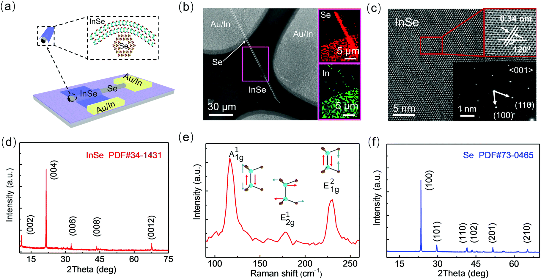 | ||
| Fig. 1 Crystal structure and characterization of InSe nanosheets and Se nanotubes. (a) Schematic diagram of the Se/InSe p–n heterojunction device. Inset: The atomic structure for the cross-section of the heterojunction. (b) SEM image of the InSe/Se heterojunction device and EDX mapping of the Se and In elements. (c) HRTEM image of the InSe nanosheets. Inset: The corresponding reverse Fourier transform pattern and SAED pattern with an orientation along the [001] zone axis. (d) XRD spectrum of the InSe nanosheets. (e) Raman spectrum of the InSe nanosheets. (f) XRD spectrum of the Se nanotubes. | ||
Results and discussion
Fig. 1a demonstrates the schematic configuration of the 1D Se–2D InSe hybrid van der Waals p–n heterojunctions, which was constructed by the polydimethylsiloxane (PDMS)-assisted dry alignment transfer method. In this configuration, 2D InSe nanosheets were synthesized by Bridgeman and mechanical exfoliation methods.33 And 1D Se nanotubes were synthesized by the chemical vapor deposition (CVD) method. The device fabrication process is shown in Fig. S1 and S2 (ESI†), and detailed descriptions of the fabrication process are given in the methods section. Scanning electron microscopy (SEM) images and energy dispersive spectra (EDS) maps of each element (Fig. 1b and Fig. S3, S4, ESI†) demonstrate that the 2D nanosheets and 1D nanotubes were InSe and Se, respectively with a smooth neat surface and a uniform diameter. The lateral size of the InSe nanosheets and the length of the Se nanotubes are about 50 and 100 μm, respectively. SEM and AFM measurement demonstrates that the height of the nanotube is around 1 μm and the thickness of the InSe nanosheet is about 30 nm (Fig. S4 and S5, ESI†). The InSe crystal has mainly three different phases, which are γ, ε, and β based on stacking the primitive layers in different sequences.44 Therefore, it is necessary to determine the crystallographic phase of the synthesized InSe samples. And the structure of the synthesized InSe was first identified and characterized by transmission electron microscopy (TEM). Fig. 1c is the TEM (HRTEM) image and selected area electron diffraction (SAED) pattern. It can be found that in Fig. 1c, the synthesized InSe sample has a hexagonal lattice structure with the [001] zone axis. The lattice constant along the [100] direction is 0.40 nm, the d-spacing of the {100} plane family is 0.34 nm, and the angle between the (100) and (010) crystallographic planes is 120°. Our synthesized InSe samples possess the same hexagonal lattice (a = b = 4.05 Å, c = 16.93 Å) as that of β or ε-InSe. Then, we further characterized the structural characterizations of the InSe sample by X-ray diffraction (XRD). As shown in Fig. 1d, there are only five peaks in the XRD pattern of the prepared InSe sample (10.84°, 21.56°, 32.47°, 43.7°, 67.7°), which is consistent with the crystal faces (002, 004, 006, 008, 0012) of the hexagonal crystal structure of β or ε-InSe corresponding of the standard database (PDF# 34-1431). In order to confirm the phase of our InSe samples, Raman spectroscopy was characterized to further determine the lattice vibration modes of the InSe nanosheets. As shown in Fig. 1e, three peaks located at 116.6 cm−1, 117.6 cm−1, and 228.1 cm−1 agreed well with the phonon modes of A11g, E12g and A21g. It is worth pointing out that these typical Raman modes only appear in the centrosymmetric structure of β-InSe.35 At the same time, the phases of the as prepared Se nanotubes are also confirmed by XRD. As shown in Fig. 1f, the peaks located at 23.4°, 29.5°, 41.4°, 43.6°, 51.6°, and 65.2° agreed well with the crystal faces (100, 101, 110, 102, 201, 210) of the t-Se (PDF# 06-0362). In addition, the sharp diffraction peaks demonstrate good crystallinity of our Se samples.In order to explore the usefulness of the p-Se/n-InSe heterojunction in high-performance self-powered photodetectors, the I–V curve of the p-Se/n-InSe heterojunction was characterized ranging from −5 V to 5 V at first. The inset of Fig. 2a is the optical microscope image of the p-Se/n-InSe heterojunction with In electrodes. It can be found that the I–V curve in Fig. 2a exhibited a significant rectification characteristic indicating a typical photodiode behavior. Because two types of junctions (Schottky junction and p–n junction) might exist in this vdW heterojunction device, more information is needed to get an insight into the operating mechanism. Therefore, I–V curves of both pure Se and pure InSe samples were measured under dark conditions. As shown in Fig. 2b, the linear characteristic of the dark I–V curve indicating Se–In is an excellent ohmic contact. Fig. 2c shows the I–V plots from In–InSe–In contact; a lower current is found and it exhibits smaller symmetric back-to-back Schottky contact properties. The above results suggested that the large rectifying property in Fig. 2a is mainly originated from the p–n heterojunction between Se and InSe instead of the metal–semiconductor contacts. And the diode possesses a high rectification factor of ∼102 under |voltage| = 5 V (23 nA @ 5 V; 20 pA @ −5 V).
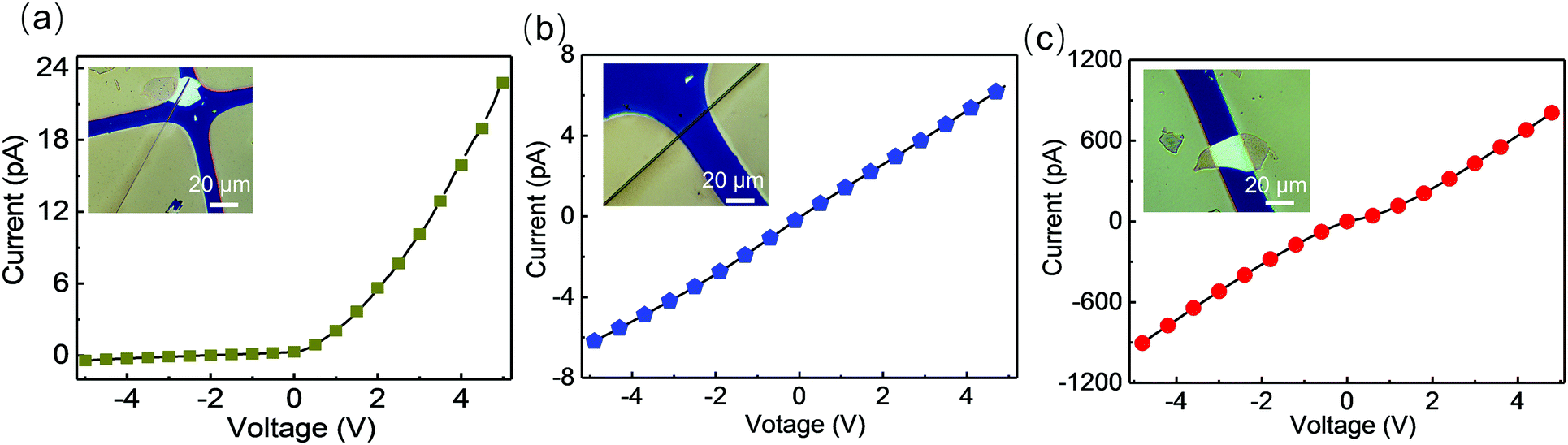 | ||
| Fig. 2 Design of the Se/InSe mixed-dimensional heterojunction, Se and InSe devices with In electrodes. (a) I–V curve of the Se/InSe p–n heterojunction. (b) The I–V curve of the Se device. (c) The I–V curve of the InSe device. Inset: The corresponding optical microscope images of the Se/InSe mixed-dimensional heterojunction, Se and InSe devices. | ||
To examine the photovoltaic property of this diode, on/off cycles of the Se/InSe hybrid p–n junction device were characterized under different illuminations in the UV-visible region at 0 V. As shown in Fig. 3a, the currents of the diode could change immediately with good reproducibility and highly stability (an amplificatory dark current of the Se/InSe hybrid p–n junction diode is shown in Fig. S6, ESI†) when the light switched between on and off. In particular, the photo-dark current ratio could reach up to 2 orders of magnitude at the wavelength of 450 nm. To further explore the signal-to-noise ratio of the diode, linear dynamic range (LDR, typically quoted in dB) could be obtained from the equation:
LDR = 20![[thin space (1/6-em)]](https://www.rsc.org/images/entities/char_2009.gif) log(Ip/Id) log(Ip/Id) | (1) |
| Ip = Iillumination − Idark | (2) |
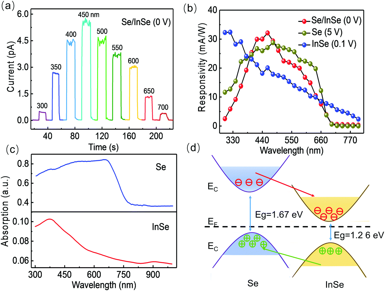 | ||
| Fig. 3 Optoelectronic characterization and energy band structure of the Se/InSe heterojunction. (a) Time-dependent photocurrent of the Se/InSe photodetector under 300–700 nm light illumination (P = 1.05 mW cm−2) at zero bias voltage. (b) Spectra responsivity of Se/InSe at 0 V, Se at 5 V and InSe at 0.1 V under 300–800 nm light illumination with P = 1.05 mW cm−2. (c) Absorption spectra of InSe nanosheets and Se nanotubes. (d) Energy band diagram of the Se/InSe heterojunction under light illumination. | ||
It is the difference between the illumination current and dark current. The calculated LDR (63 dB) obtained at a wavelength of 450 nm (3 mW cm−2) is comparable to InGaAs based photodetectors (66 dB).
In order to explore the working wavelength range of the p–n junction self-powered photodetector, the responsivity (Rλ) was calculated by the equation:
| Rλ = Ip/P | (3) |
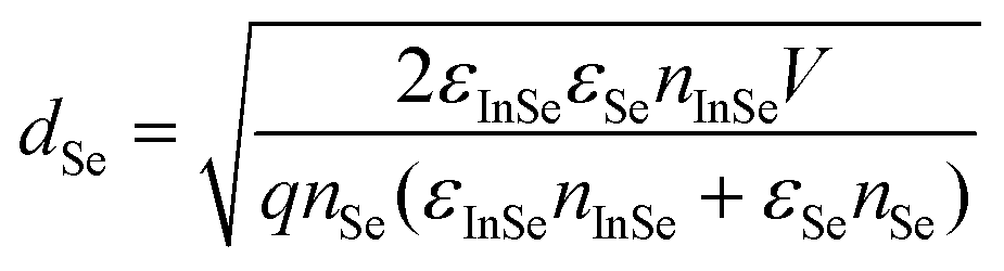
As shown in Fig. 3b, the photodetector displays a broadband photoresponse in the UV-visible region at zero bias voltage. It can be found that the maximum responsivity could reach up to 35 mA W−1 at 460 nm, which is comparable to that of the pristine Se device at 5 V and InSe device at 0.1 V, respectively. However, unlike the broadband responsivity of the Se/InSe p–n junction and pristine Se device, the responsivity of the pristine InSe device decreased dramatically in the visible region. However, the photoluminescence (PL) results of the Se and InSe samples (Fig. S7, ESI†) correspond well with the band gap of InSe (1.26 eV) and Se (1.67 eV), respectively. To get further insights into this abnormal phenomenon of the pristine InSe photodetector, the absorption curves of both the InSe nanosheets and Se nanotubes were characterized as well. As shown in Fig. 3c, the absorption of InSe decreases dramatically with increasing wavelength, which indicates the lower absorption coefficients in the long-wavelength region of 550–950 nm. Hence, the abnormal spectral responsivity of the pristine InSe device may arise from the intrinsic absorption properties of InSe nanosheets. And the same phenomena were also observed in our and other previous reports.33 To further explore the main factors for the range of spectrum response and working mechanism of the Se/InSe mix-dimensional p–n junction device, the Se and InSe depletion regions (dSe and dInSe) can be determined as45
 | (4) |
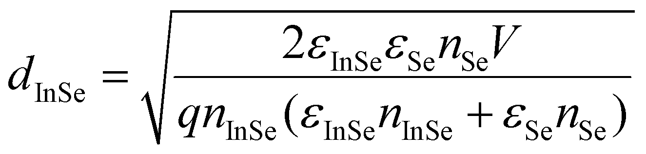 | (5) |
Here, ε is the dielectric constant (εInSe is 7.6 × 8.85 × 10−12 F m−1 and εSe is 6.3 × 8.85 × 10−12 F m−1),46,47q is the elementary charge and V is the built-in voltage (∼0.9 V). The carrier concentrations of Se and InSe are about 1014 cm−3 and 1017 cm−3, respectively.48,49 Therefore, the calculated dSe and dInSe are ∼2.5 μm and ∼2.5 nm, respectively. Therefore, the photocurrent of the Se/InSe p–n junction in this work may be mainly originating from the photocarriers of the Se nanotubes. Although the photocarriers can be generated in InSe depletion, the photocurrent of the Se/InSe p–n junction in this work mainly originates from the photocarriers of the Se nanotube. Therefore, the working wavelength of the Se/InSe photodetector is similar to that of the pristine Se device instead of the pristine InSe device. As shown in the energy-band diagram of Fig. 3d, the electron affinities (χ) of Se and InSe are 3.2 eV and 4.02 eV,33,50 and the corresponding band gaps are 1.67 and 1.26 eV, respectively.
Considering the dangling bond-free surface of the 2D layered flexible InSe nanosheets, InSe nanosheets are fabricated on the upper layer of our mixed-dimensional heterojunction (Fig. 1a). This architecture not only can isolate Se from the outside environment, but also can enhance the area of the p–n junction. Therefore, after the InSe nanosheet was coated on the surface of the Se nanotube, the built-in electric field was formed at the interface of the Se and InSe semiconductors. And a typical type-II p–n junction is formed as well. Under light illumination, the photogenerated electron–hole pairs could be separated efficiently by built-in electric field, the electrons move towards the InSe conduction band and the holes move towards the Se valence band, leading to the formation of photovoltages at the interface, and the responsivity can be enhanced. Therefore, the self-powered Se/InSe photodetector exhibits high photocurrent, large on/off ratio, and broadband response. Such broadband photodetectors would satisfy the requirements of broadband light communication, imaging sensing, etc.
In addition, photoswitching characteristics of the p-Se/n-InSe heterojunction self-powered photodetectors were systematically investigated under different light intensities at the wavelength of 400 nm, 500 nm and 460 nm, respectively. As shown in Fig. 4a–c, a steadily increasing photocurrent response with increasing light intensity is observed for the aforementioned three wavelengths. It is consistent with the fact that the number of photogenerated carrier is proportional to the absorbed photon flux. Benefiting from the excellent hybrid p–n junction, the device exhibited a high on/off ratio of 103 at the wavelength of 460 nm with a relatively weak light intensity (3 mW cm−2). The relation between photocurrent and light power density is often fitted with a power function. It can be usually expressed as Iph ∝ APα,39,51 where A is a constant for a certain wavelength, and the exponent (0.5 < θ < 1) determines the response of the photocurrent to light intensity. As shown in Fig. 4d–f, α of the p–n junction device was calculated to be 0.66, 0.72 and 0.68 at the wavelength of 400 nm, 500 nm and 460 nm, respectively. This fractional power dependence indicates that there may be a complex electron–hole generation, trapping, and recombination process in the mixed-dimensional p–n junction device.52
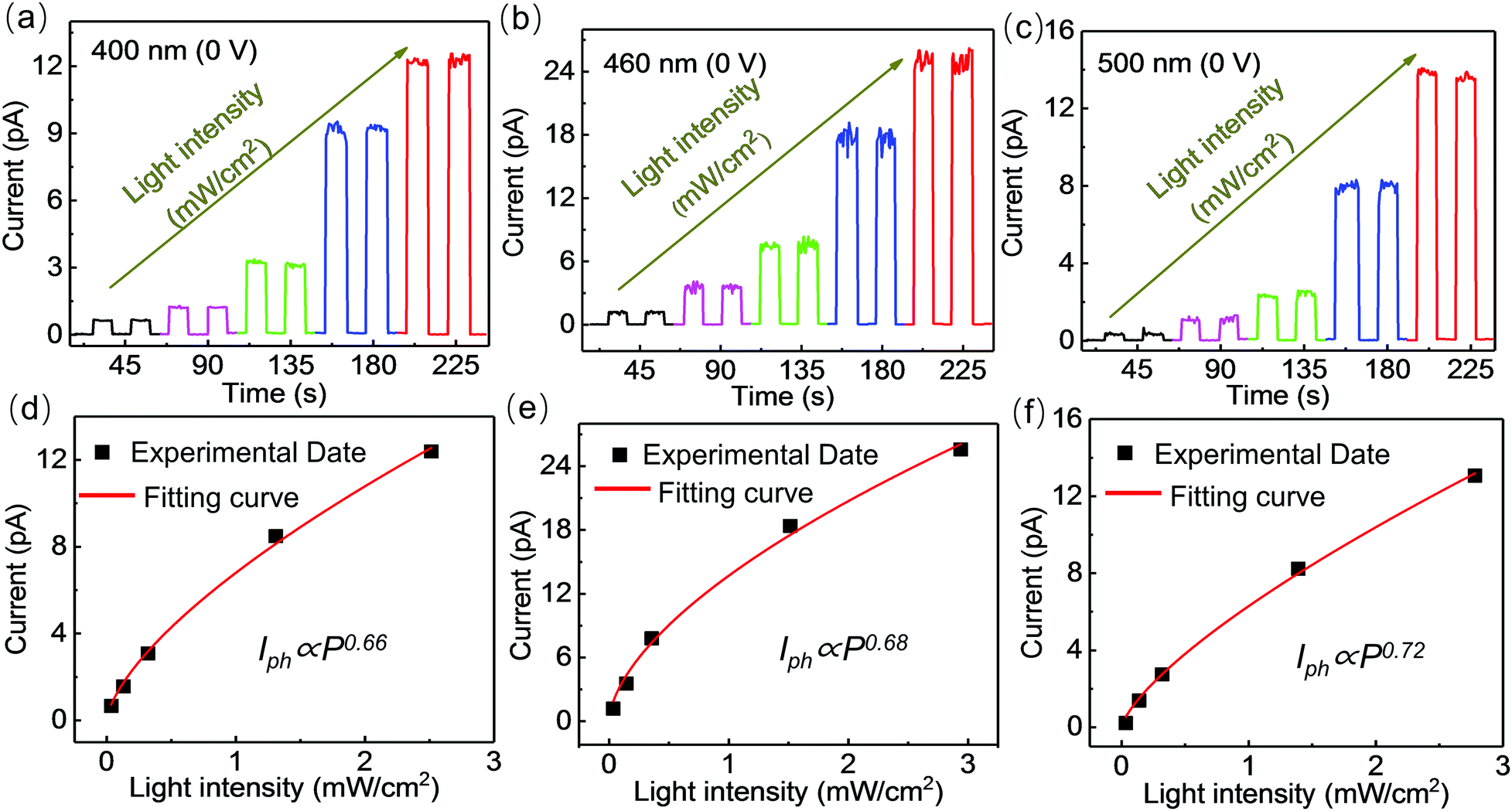 | ||
| Fig. 4 Photoresponse of the Se/InSe heterojunction under different light intensities. (a–c) Time-dependent photocurrent of the Se/InSe photodetector under 400 nm, 460 nm and 500 nm light illumination at zero bias voltage with different light intensities. (d–f) The corresponding fitting curves for the relationship between the photocurrents and the light intensities. | ||
In order to further study the impact of light intensity on the mixed-dimensional self-powered photodetector, the responsivity and associated external quantum efficiency (EQE) as a function of light intensity at the wavelength of 460 nm were also recorded. As shown in Fig. 5a and b, values of the responsivity (Rλ) and EQE decrease nonlinearly as the illumination power (P) increases. And they can reach up to 110 mA W−1 and 51% under light intensity P = 40 μW cm−2 at zero bias voltage. Then, it gradually declined from 110 to 28 mA W−1 with the light power density rising from 0.04 to 3 mW cm−2. In addition, due to our monochromator of 68 × 68 mm slit and 2.3 nm mm−1 reciprocal dispersion at the slit, the used light power range can be converted to irradiance range from 0.03 to 3 mW cm−2, corresponding with the common sunlight irradiance reaching the earth's surface.53
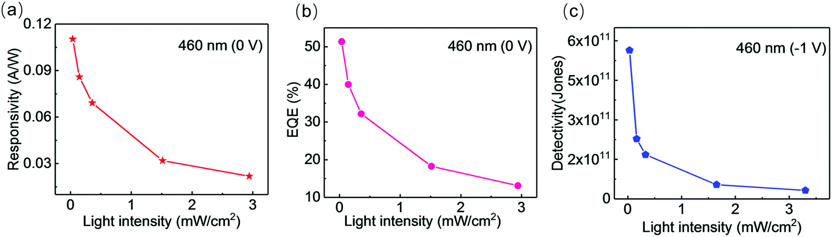 | ||
| Fig. 5 High performance of the self-powered Se/InSe photodetector. (a) The calculated responsivity of the Se/InSe photodetector under 460 nm light illumination with different light intensities at zero bias voltage. (b) The calculated EQE of the Se/InSe photodetector under 460 nm light illumination with different light intensities at zero bias voltage. (c) The calculated detectivity of the Se/InSe photodetector under 460 nm light illumination with different light intensities at −1 V. | ||
The detectivity (D*) is another key figure-of-merit for a photodetector, which is defined as the ability of detecting the smallest signal. As the shot noise is considered as the major component in total noise, D* could be expressed as54
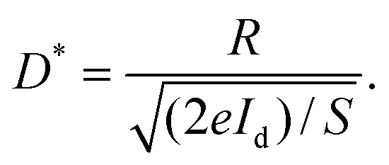 | (6) |
In order to investigate the stability of the p–n junction self-powered photodetector, reproducible on/off switching of Se/InSe p–n junction photodetector at 0 V, pristine Se device under a bias of 5 V, and pristine InSe device under a bias of 0.1 V was characterized upon 460 nm (3 mW cm−2) light, respectively. As shown in Fig. 6a, the current of the Se/InSe p–n junction photodetector rapidly increased and maintained a stable state under illumination. A switching cycle in a high time resolution mode is shown in Fig. 6b, the rise time in which the photocurrent increased from 10% to 90% is 30 ms, and the fall time in which it decreased from 90% to 10% is 37 ms, indicating that the self-powered photodetector has a fast response speed. These values are one order of magnitude faster than that of the pristine InSe and Se device even at a bias voltage (Fig. 6c–f). Therefore, in addition to the built-in electric field of the p–n junction, the photoexcited electron–hole pairs could be separated more efficiently. The fast speed of the mixed-dimensional p–n junction device may also be attributed to the upper surface dangling-bond-free surface of the two dimensional InSe materials, and O2 or H2O molecules are hindered to adhere to the Se surface. And the persistent photoconductivity effect would be avoided in this case,55 and the response time can be faster.
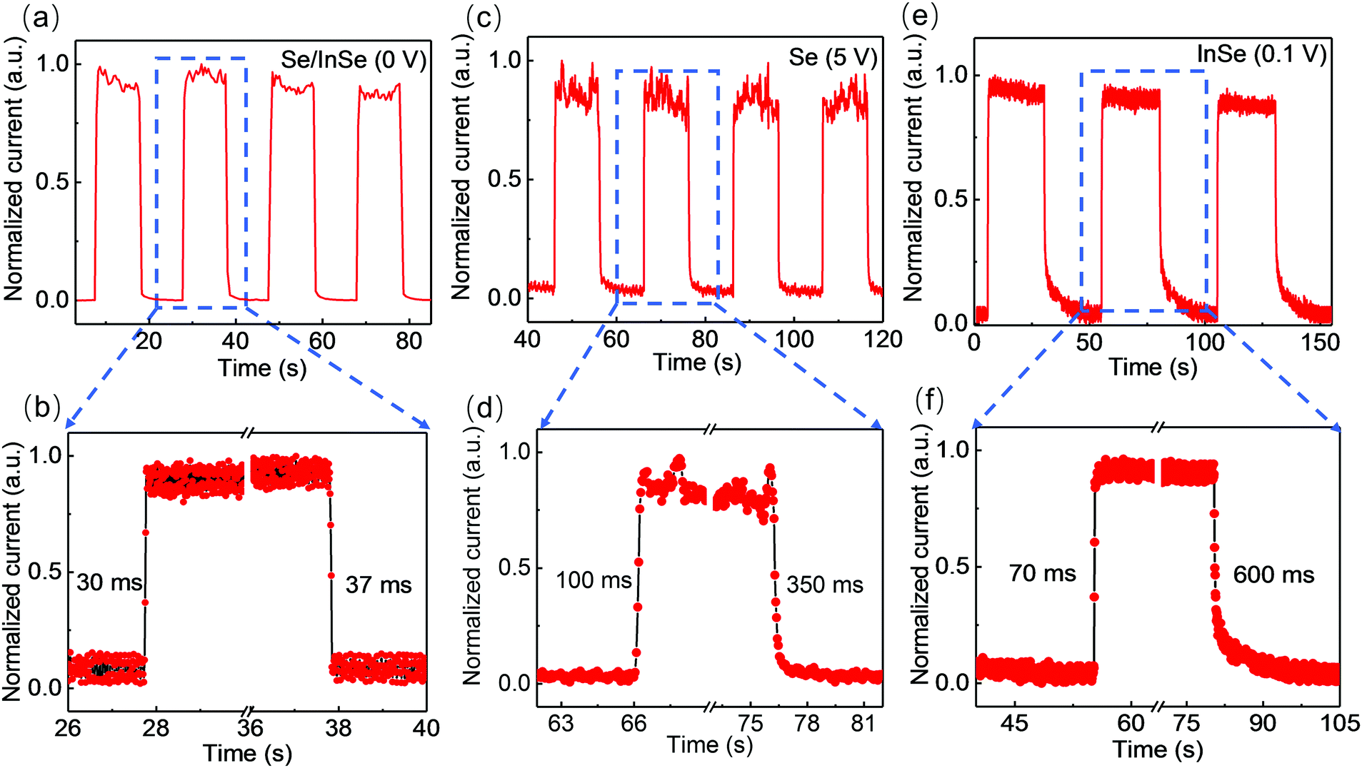 | ||
| Fig. 6 Photoresponse speed of Se/InSe, Se and InSe photodetector. (a) Time-dependent photocurrent of Se/InSe under 460 nm light illumination at 0 V. (b) One cycle of the photoresponse to a wavelength of 460 nm for estimating both the rise and fall time of (a). (c) Time-dependent photocurrent of Se under 460 nm light illumination at 5 V. (d) One cycle of the photoresponse to a wavelength of 460 nm for estimating both the rise and fall time of (c). (e) Time-dependent photocurrent of InSe under 460 nm light illumination at 0.1 V. (f) One cycle of the photoresponse to a wavelength of 460 nm for estimating both the rise and fall time of (e). | ||
In order to show the excellent performance of the Se/InSe self-powered photodetector more intuitively, comparison between the mix-dimensional p–n heterojunction photodetector in this work and other previous devices is proposed. As shown in Table 1, the comprehensive performance of our Se/InSe self-powered photodetector is significantly better than that of other Se or InSe based traditional heterojunction photodetectors (e.g. Se/PEDOT, Se/n-Si, BP/InSe, InSe/GaTa).27,50,56,57 And the responsivities, and on/off ratios (Ilight/Idark) are also larger than that of 1D–2D mixed-dimensional structure devices (ZnO/WSe2, CdS/MoTe2).29,58
| Photodetector | Dimensionality | Wavelength | V ds (V) | R (mA W−1) | D* (Jones) | On/off | EQE (%) | τ r/τd (ms) | Ref. |
|---|---|---|---|---|---|---|---|---|---|
| InSe/Se | 2D/1D | 460 nm, 1 mW cm−2 | 0 | 32 | 1.7 × 10¹¹ | 500 | 8.7 | 30/37 | This work |
| Se/PEDOT | 1D/1D | 450 nm, 1.03 mW cm−2 | 0 | ≈3 | 50 | ≈1 | 1/10 | 50 | |
| Se/n-Si | 1D/3D | 500 nm, 1.71 mW cm−2 | −2 | 25 | 1011 | ≈100 | 7 | 0.2/1.8 | 56 |
| BP/InSe | 2D/2D | 455 nm, 12.8 W mm−2 | 0.5 | 11.7 | 60 | 3.2 | 24/32 | 27 | |
| InSe/GaTa | 2D/2D | 405 nm, 0.16 mW cm−2 | 0 | 13.8 | 4.2 | 0.02 | 57 | ||
| MoTe2/CdS | 2D/1D | 470 nm, 0.5 mW cm−2 | 0 | ≈11 | 50 | 58 | |||
| WSe2/ZnO | 2D/1D | 470 nm, 2.6 mW cm−2 | −5 | 530 | 29 |
Conclusions
In summary, a mixed-dimensional heterojunction was fabricated by a p-Se nanotube and n-InSe nanosheet, and the heterojunction can work as a self-powered photodetector with a high responsivity range from the UV to visible region. In addition, the mixed-dimensional van der Waals heterojunction exhibited high on/off ratios (103) at a relatively weak light intensity of 3 mW cm−2. Under 460 nm illumination, the responsivity can reach up to 110 mA W−1 without any power supply, which is higher than that of other mix-dimensional photodetectors based on similar materials or structure. And this value is comparable to that of the pristine Se device at 5 V and the InSe device at 0.1 V, respectively. The mixed-dimension heterojunction not only expands the selectivity of the materials for constructing photodetectors, but also increases the opportunities of two-dimensional material applications. It is believed that the 1D–2D mixed-dimensional heterojunctions proposed herein would provide a novel pathway for fabricating high resolution, flexibility and transparent photovoltaics/photoelectric devices.Experimental
Device fabrication
InSe nanosheets were fabricated by the Bridgeman and mechanical exfoliation methods. Se nanotubes were fabricated by the chemical vapor deposition method. The process of fabricating InSe nanosheets and Se nanotubes is demonstrated in our previous papers,33,41 and the construction of InSe/Se heterojunction photodetectors is detailed below. Se nanotubes were transferred on to the SiO2/Si substrate assisted by ethanol solution, and then they were annealed at 120 °C for 0.5 h in an argon protected environment to remove any residual solutions. Subsequently, the InSe nanosheet was transferred directionally onto the target Se nanotube assisted by a PDMS film under an optical microscope. Finally, two Au/In (10 nm/30 nm) electrodes were fabricated by thermal evaporation with a shadow mask.Characterization
SEM (Hitachi S-4200) and AFM (Bruker Dimension Icon) were performed to characterize the morphology and structure of the samples. The composition of the InSe and Se samples was determined by EDS. The structure and optical properties of the samples were identified by XRD (DIFFRACTOMETER-6000), TEM (Tacnai-G2 F30), confocal Raman spectroscopy (LabRAM XploRA, laser wavelength is 532 nm for InSe, 638 nm for Se), and a UV-vis spectrophotometer (Hitachi U-4100). The electrical and photoelectric properties of the photodetector were evaluated using a program-controlled semiconductor characterization system (Keithley 4200-PA SCS), a xenon lamp (Gloria-X150A), a probe station (Lakeshore), and a monochromator (Zolix, Omni-λ300i), respectively. All the measurements were performed at room temperature.Conflicts of interest
The authors declare no conflicts of interest.Acknowledgements
This work is supported by the National Natural Science Foundation of China (No. 61390502, 61874037, 61505033, and 21825103), the Foundation for Innovative Research Groups of the National Natural Science Foundation of China (No. 51521003), the National Postdoctoral Science Foundation of China (No. 2017M621254, 2018T110280), Heilongjiang Provincial Postdoctoral Science Foundation (No. LBH-TZ1708), Self-Planned Task of State Key Laboratory of Robotics and System (HIT) (No. SKLRS201607B), Key Laboratory of Microsystems and Microstructures Manufacturing of Ministry of Education (HIT) (No. 2017KM003), and Fundamental Research Funds for the Central Universities (No. HIT.NSRIF.2019060).Notes and references
- L. Su, W. Yang, J. Cai, H. Chen and X. Fang, Small, 2017, 13, 1701687 CrossRef PubMed.
- Z. Xu, S. Lin, X. Li, S. Zhang, Z. Wu, W. Xu, Y. Lu and S. Xu, Nano Energy, 2016, 23, 89–96 CrossRef CAS.
- Y. Zhang, W. Xu, X. Xu, W. Yang, S. Li, J. Chen and X. Fang, Nanoscale Horiz., 2019, 4, 452–456 RSC.
- M. Kumar, M. Patel, H.-S. Kim, J. Kim and J. Yi, ACS Appl. Mater. Interfaces, 2017, 9, 38824–38831 CrossRef CAS PubMed.
- W. Wu, Q. Zhang, X. Zhou, L. Li, J. Su, F. Wang and T. Zhai, Nano Energy, 2018, 51, 45–53 CrossRef CAS.
- P. Luo, F. Zhuge, Q. Zhang, Y. Chen, L. Lv, Y. Huang, H. Li and T. Zhai, Nanoscale Horiz., 2019, 4, 26–51 RSC.
- Y. Zhang, W. Xu, X. Xu, J. Cai, W. Yang and X. Fang, J. Phys. Chem. Lett., 2019, 10, 836–841 CrossRef CAS PubMed.
- R. Dong, C. Lan, F. Li, S. Yip and J. C. Ho, Nanoscale Horiz., 2019, 4, 1342–1352 RSC.
- H. Wang, H. Chen, L. Li, Y. Wang, L. Su, W. Bian, B. Li and X. Fang, J. Phys. Chem. Lett., 2019, 10, 6850–6856 CrossRef CAS PubMed.
- H. Fang and W. Hu, Adv. Sci., 2017, 4, 1700323 CrossRef PubMed.
- L. Shi, F. Wang, B. Li, X. Chen, B. Yao, D. Zhao and D. Shen, J. Mater. Chem. C, 2014, 2, 5005–5010 RSC.
- K. Kim, J. Kang, M. Lee, C. Yoon, K. Cho and S. Kim, Jpn. J. Appl. Phys., 2010, 49, 06GG05 Search PubMed.
- D. Wu, Y. Jiang, X. Yao, Y. Chang, Y. Zhang, Y. Yu, Z. Zhu, Y. Zhang, X. Lan and H. Zhong, J. Mater. Chem. C, 2014, 2, 6547–6553 RSC.
- M. Z. Bellus, Z. Yang, P. Zereshki, J. Hao, S. P. Lau and H. Zhao, Nanoscale Horiz., 2019, 4, 236–242 RSC.
- C. Mu, J. Xiang and Z. Liu, J. Mater. Res., 2017, 32, 4115–4131 CrossRef CAS.
- Z. Yin, H. Li, H. Li, L. Jiang, Y. Shi, Y. Sun, G. Lu, Q. Zhang, X. Chen and H. Zhang, ACS Nano, 2011, 6, 74–80 CrossRef PubMed.
- D.-H. Kwak, P. Ramasamy, Y.-S. Lee, M.-H. Jeong and J.-S. Lee, ACS Appl. Mater. Interfaces, 2019, 11, 29041–29046 CrossRef CAS PubMed.
- S. C. Dhanabalan, J. S. Ponraj, H. Zhang and Q. Bao, Nanoscale, 2016, 8, 6410–6434 RSC.
- D. Kufer, I. Nikitskiy, T. Lasanta, G. Navickaite, F. H. Koppens and G. Konstantatos, Adv. Mater., 2015, 27, 176–180 CrossRef CAS PubMed.
- P. Xiao, J. Mao, K. Ding, W. Luo, W. Hu, X. Zhang, X. Zhang and J. Jie, Adv. Mater., 2018, 30, 1801729 CrossRef PubMed.
- D.-S. Um, Y. Lee, S. Lim, S. Park, H. Lee and H. Ko, ACS Appl. Mater. Interfaces, 2016, 8, 33955–33962 CrossRef CAS PubMed.
- L. Ye, H. Li, Z. Chen and J. Xu, ACS Photonics, 2016, 3, 692–699 CrossRef CAS.
- R. Cheng, D. Li, H. Zhou, C. Wang, A. Yin, S. Jiang, Y. Liu, Y. Chen, Y. Huang and X. Duan, Nano Lett., 2014, 14, 5590–5597 CrossRef CAS PubMed.
- F. Yan, L. Zhao, A. Patanè, P. Hu, X. Wei, W. Luo, D. Zhang, Q. Lv, Q. Feng and C. Shen, Nanotechnology, 2017, 28, 27LT01 CrossRef PubMed.
- A. Islam, J. Lee and P. X.-L. Feng, ACS Photonics, 2018, 5, 2693–2700 CrossRef CAS.
- Q. A. Vu, J. H. Lee, V. L. Nguyen, Y. S. Shin, S. C. Lim, K. Lee, J. Heo, S. Park, K. Kim and Y. H. Lee, Nano Lett., 2016, 17, 453–459 CrossRef PubMed.
- S. Zhao, J. Wu, K. Jin, H. Ding, T. Li, C. Wu, N. Pan and X. Wang, Adv. Funct. Mater., 2018, 28, 1802011 CrossRef.
- H. Xue, Y. Wang, Y. Dai, W. Kim, H. Jussila, M. Qi, J. Susoma, Z. Ren, Q. Dai and J. Zhao, Adv. Funct. Mater., 2018, 28, 1804388 CrossRef.
- Y. T. Lee, P. J. Jeon, J. H. Han, J. Ahn, H. S. Lee, J. Y. Lim, W. K. Choi, J. D. Song, M. C. Park and S. Im, Adv. Funct. Mater., 2017, 27, 1703822 CrossRef.
- L. Wang, J. Jie, Z. Shao, Q. Zhang, X. Zhang, Y. Wang, Z. Sun and S. T. Lee, Adv. Funct. Mater., 2015, 25, 2910–2919 CrossRef CAS.
- P. Lin, L. Zhu, D. Li, L. Xu and Z. L. Wang, Nanoscale, 2018, 10, 14472–14479 RSC.
- G. Sun, B. Li, J. Li, Z. Zhang, H. Ma, P. Chen, B. Zhao, R. Wu, W. Dang and X. Yang, Nano Res., 2019, 12, 1139–1145 CrossRef CAS.
- M. Dai, H. Chen, R. Feng, W. Feng, Y. Hu, H. Yang, G. Liu, X. Chen, J. Zhang and C.-Y. Xu, ACS Nano, 2018, 12, 8739–8747 CrossRef CAS PubMed.
- S. R. Tamalampudi, Y.-Y. Lu, R. Kumar U, R. Sankar, C.-D. Liao, K. Moorthy B, C.-H. Cheng, F. C. Chou and Y.-T. Chen, Nano Lett., 2014, 14, 2800–2806 CrossRef CAS PubMed.
- M. Dai, H. Chen, F. Wang, Y. Hu, S. Wei, J. Zhang, Z. Wang, T. Zhai and P. Hu, ACS Nano, 2019, 13, 7291–7299 CrossRef CAS PubMed.
- S. Lei, F. Wen, L. Ge, S. Najmaei, A. George, Y. Gong, W. Gao, Z. Jin, B. Li and J. Lou, Nano Lett., 2015, 15, 3048–3055 CrossRef CAS PubMed.
- W. Feng, W. Zheng, W. Cao and P. Hu, Adv. Mater., 2014, 26, 6587–6593 CrossRef CAS PubMed.
- C. Habenicht, M. Knupfer and B. Büchner, Phys. Rev. B: Condens. Matter Mater. Phys., 2015, 91, 245203 CrossRef.
- L. Zheng, K. Hu, F. Teng and X. Fang, Small, 2017, 13, 1602448 CrossRef PubMed.
- J. Qin, G. Qiu, J. Jian, H. Zhou, L. Yang, A. Charnas, D. Y. Zemlyanov, C.-Y. Xu, X. Xu and W. Wu, ACS Nano, 2017, 11, 10222–10229 CrossRef CAS PubMed.
- K. Hu, H. Chen, M. Jiang, F. Teng, L. Zheng and X. Fang, Adv. Funct. Mater., 2016, 26, 6641–6648 CrossRef CAS.
- W. Deng, C. You, X. Chen, Y. Wang, Y. Li, B. Feng, K. Shi, Y. Chen, L. Sun and Y. Zhang, Small, 2019, 15, 1901544 CrossRef PubMed.
- Y. Liu, F. Wang, X. Wang, X. Wang, E. Flahaut, X. Liu, Y. Li, X. Wang, Y. Xu and Y. Shi, Nat. Commun., 2015, 6, 8589 CrossRef CAS PubMed.
- Z. Yang, W. Jie, C.-H. Mak, S. Lin, H. Lin, X. Yang, F. Yan, S. P. Lau and J. Hao, ACS Nano, 2017, 11, 4225–4236 CrossRef CAS PubMed.
- L. Su, Q. Zhang, T. Wu, M. Chen, Y. Su, Y. Zhu, R. Xiang, X. Gui and Z. Tang, Appl. Phys. Lett., 2014, 105, 072106 CrossRef.
- D. Errandonea, A. Segura, V. Munoz and A. Chevy, Phys. Rev. B: Condens. Matter Mater. Phys., 1999, 60, 15866 CrossRef CAS.
- A. Lakatos and M. Abkowitz, Phys. Rev. B: Solid State, 1971, 3, 1791 CrossRef.
- J. Heleskivi, T. Stubb and T. Suntola, J. Appl. Phys., 1969, 40, 2923–2927 CrossRef CAS.
- M. Parlak, C. Ercelebi, I. Günal, Z. Salaeva and K. Allakhverdiev, Thin Solid Films, 1995, 258, 86–90 CrossRef CAS.
- P. Yu, K. Hu, H. Chen, L. Zheng and X. Fang, Adv. Funct. Mater., 2017, 27, 1703166 CrossRef.
- Q. Hong, Y. Cao, J. Xu, H. Lu, J. He and J.-L. Sun, ACS Appl. Mater. Interfaces, 2014, 6, 20887–20894 CrossRef CAS PubMed.
- H. Kind, H. Yan, B. Messer, M. Law and P. Yang, Adv. Mater., 2002, 14, 158–160 CrossRef CAS.
- H. Chen, K. Liu, L. Hu, A. A. Al-Ghamdi and X. Fang, Mater. Today, 2015, 18, 493–502 CrossRef CAS.
- W. Y. Kong, G. A. Wu, K. Y. Wang, T. F. Zhang, Y. F. Zou, D. D. Wang and L. B. Luo, Adv. Mater., 2016, 28, 10725–10731 CrossRef CAS PubMed.
- N. Zhou, R. Wang, X. Zhou, H. Song, X. Xiong, Y. Ding, J. Lü, L. Gan and T. Zhai, Small, 2018, 14, 1702731 CrossRef PubMed.
- W. Yang, K. Hu, F. Teng, J. Weng, Y. Zhang and X. Fang, Nano Lett., 2018, 18, 4697–4703 CrossRef CAS PubMed.
- W. Feng, Z. Jin, J. Yuan, J. Zhang, S. Jia, L. Dong, J. Yoon, L. Zhou, R. Vajtai and J. M. Tour, 2D Mater., 2018, 5, 025008 CrossRef.
- M. Y. Lu, Y. T. Chang and H. J. Chen, Small, 2018, 14, 1802302 CrossRef PubMed.
Footnote |
| † Electronic supplementary information (ESI) available. See DOI: 10.1039/c9nh00705a |
| This journal is © The Royal Society of Chemistry 2020 |