DOI:
10.1039/C9NH00431A
(Communication)
Nanoscale Horiz., 2020,
5, 144-149
Transfer printing of polymer light-emitting devices with a small molecular seeding layer featuring thermally activated delayed fluorescence for triplet harvesting†
Received
1st July 2019
, Accepted 23rd August 2019
First published on 24th August 2019
Abstract
Transfer printing (TP) technology is capable of fabricating arbitrary thin-films on desired seeding layers or substrates. Here, we employed the TP scheme on a small molecule based hole transporting layer (HTL) as well as a seeding layer to demonstrate a multilayered structure for polymer light-emitting diodes (PLEDs), without the requirement of an orthogonal spin-coating process. To enhance the electroluminescence performance of the fluorescent polymer, poly(para-phenylene vinylene) (Super Yellow, SY), a thermally activated delayed fluorescence (TADF) molecule, 10,10′-(4,4′-sulfonylbis(4,1-phenylene))bis(9,9-dimethyl-9,10-dihydroacridine) (DMAC-DPS), was utilized as the TP seeding layer, which resulted in preferential triplet harvesting and hole transporting, and alleviated exciton quenching, simultaneously. Without the interfacial mixing effect of the small molecular HTL and TP-SY, the state-of-the-art PLED with the fluorescent polymer acquired a considerably high current efficiency of 16.6 cd A−1, which exhibited an almost two-fold enhancement with respect to the standard device with spin-coated SY (8.5 cd A−1). Such TP devices open a new door for developing solution-processed devices with unlimited design of multilayered architectures which are usually restricted by the interfacial mixing effect and the choice of the orthogonal solution.
New concepts
Transfer printing (TP) is of intrinsic superiority in the multilayered solution process of organic optoelectronic devices, which overcomes the interfacial mixing effect without applying complicated cross-linking and orthogonal solvent strategies. We managed to construct a multilayered state-of-the-art polymer light-emitting device based on TP technology. A small molecule based hole transporting layer (HTL), which is typically not feasible beneath the polymer due to the intermixing effect in a non-orthogonal solvent, was used as the seeding layer to deposit the light-emitting polymer. Because of the nature of thermally activated delayed fluorescence of the HTL, it could reduce the interfacial quenching and harvest triplet excitons via reverse intersystem crossing and subsequently transfer singlet excitons via Förster resonant energy transfer to the polymer processed by TP. The surface energy and work of adhesion dominating the TP process were precisely controlled, which resulted in a distinct interface between the HTL and the polymer. Therefore, an almost two-fold enhancement of the electroluminescence efficiency was realized compared with the reference with a single-layered spin-coating polymer. This strategy opens up a new route to develop multilayered device architectures via a full solution process approach.
|
Introduction
Organic light-emitting diodes (OLEDs) with high-resolution in flat screen displays, low power consumption, small thickness and light weight, and excellent capability of folding, bending and stretching,1–3 have attracted extensive attention. Nevertheless, the high cost of manufacturing via thermal evaporation in high vacuum systems remains an obstacle in the commercialization of OLED products. Compared with vacuum evaporation, solution-process techniques, including spin-coating (SC),4,5 inkjet printing,6–12 brush coating,13 screen printing,14 blade coating,15etc., are promising for mass production with the fascinating features of low cost and production of large area materials. However, there is still a huge challenge regarding multilayered fabrication by a solution process due to the interfacial mixing effects, e.g., the underlying layer tends to be dissolved by the solvent used in the following layer.16 In order to overcome this problem, cross-linking17–21 and orthogonal solvent strategies22–29 have been developed. Unfortunately, these methods still require the synthesis of specific compounds featuring linkability, solvent compatibility, and well matched energy levels. It is hard to guarantee all the above-mentioned properties concurrently.
Transfer printing (TP) technology has been developed to overcome the difficulty in developing multilayered thin-film structures via solution processes, which successfully avoids redissolution and diffusion. In the field of organic solar cells, this technique has been used to construct multilayered devices30–33 and regulate vertical phase segregation.32,34,35 Owing to the critical demand for film uniformity and smoothness, TP used in OLEDs is challenging but meaningful. In 2007, Yim et al. first proposed the idea of employing TP to fabricate the bilayer structures of polymer hole-transporting layer (HTL)/polymer emitting layer (EML) to solve the problem of non-ideal orthogonal solvents for poly[(9,9-dioctylfluorenyl-2,7-diyl)-co-(4,4′-(N-(4-sec-butylphenyl)diphenylamine))] (TFB).36 In 2009, Lee's group demonstrated that TP polymer light-emitting diodes (PLEDs) were superior to the SC ones, especially in terms of device lifetime.37 Then the same group utilized an interlayer and TP method to realize white PLEDs.38,39 However, the EMLs in these studies were mainly the conventional fluorescence emitters, which are hardly able to utilize the triplet excitons under electrical excitation. In 2011, Park et al. improved device efficiency by transferring the phosphorescent EML onto the wide bandgap material, tris(4-carbazoyl-9-ylphenyl)amine (TcTa), compared with the SC ones.40 But the EML was directly spin-coated on PDMS, whose surface is chemically incompatible with organic solvents, causing swelling of PDMS and a non-uniform EML film.41
Recently, TADF materials have attracted widespread interest in OLEDs owing to a small energy gap (ΔEST) between triplet excited states (T1) and singlet excited states (S1), which can promote reverse intersystem crossing (RISC) from T1 to S1 and achieve 100% exciton utilization.42,43 A common and accessible method is to utilize a TADF material as a triplet harvester to sensitize the conventional fluorescence emitter, realizing high exciton utilization combined with high photoluminescence quantum yields (PLQYs) of fluorescence dopants to achieve highly efficient electroluminescence (EL). Since Adachi's and Duan's group proposed this idea of TADF-sensitized fluorescence in 2014,44,45 many researchers have followed their steps to realize dual improvements of EL efficiency and device stability.46–50 However, in the conventional devices, the host and guest were mixed in the same EML, which may activate Dexter energy transfer (DET) from the host to guest because DET depends on the short-range electron exchange.51 In order to alleviate DET, large steric hindrance has been introduced into the host45,46,52 or guest49,53 which prevents strong intermolecular interactions. Furthermore, Han et al. have proved that spatial separation of the TADF host and fluorescence guest can improve the EL performances because of DET control.50
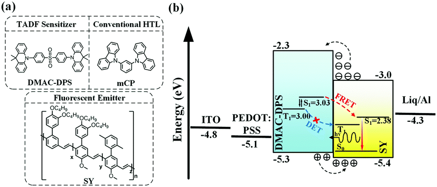
In this contribution, we present a new approach to sensitizing neat TP fluorescent polymer emitters, via the long-range Förster energy transfer from the underlying layer, i.e., a SC-HTL, 10,10′-(4,4′-sulfonylbis(4,1-phenylene))bis(9,9-dimethyl-9,10-dihydroacridine) (DMAC-DPS),54 which is a blue TADF emitter with a considerably high PLQY. In comparison, the reference SC-HTL, 1,3-di(9H-carbazol-9-yl)benzene (mCP), was also fabricated. The molecular structures of the compounds used in this work are shown in Fig. 1a. The device structure and energy level alignment are schematically illustrated in Fig. 1b. We successfully transfer-printed the fluorescent polymer, poly(para-phenylene vinylene) (Super Yellow, SY), onto small molecular HTLs as seeding layers, which were not achievable by consecutive SC processes as the small molecule-based HTLs could be washed away completely in this manner. The SC-HTL can effectively reduce the exciton quenching by the adjacent PEDOT:PSS.17 As shown in Fig. 1b, for the TADF sensitizer DMAC-DPS, the triplet excitons can be upconverted to the singlet states because of its small ΔEST. The singlet excitons could be resonantly transferred to SY via Förster energy transfer. Although some previous studies have proved that DMAC-DPS is a sensitizer in the mixed EML,57,58 it is tricky to handle the non-radiative Dexter energy transfer in host–guest doped systems as they are not well spatially separated. In contrast, the sensitizing DMAC-DPS beneath the TP-SY could preferably guarantee the long-range Förster energy transfer and restrict the short-range Dexter energy transfer, which is schematically illustrated in Fig. 1b.
 |
| | Fig. 1 (a) The molecular structures of DMAC-DPS, mCP and SY, (b) energy level alignment of the device and the EL mechanism. The singlet and triplet states, highest occupied molecular orbital (HOMO), lowest unoccupied molecular orbital (LUMO), and work function of the materials are obtained from the literature.5,59 | |
Results and discussion
First of all, the TP mechanism of SY on the small molecular HTL should be carefully handled. The thin film transfer from one substrate to the other layer is mainly dominated by the difference in the work of adhesion (T) between these two layers, which depends on the surface energy of each layer. In order to achieve the uniform TP-EML from the sacrificing glass substrate to the seeding SC-HTL (see Fig. 3(a)–(c)), the work of adhesion between the elastomeric polydimethylsiloxane (PDMS) stamp and SY should be larger than that between the glass substrate and SY, i.e., T (WPDMS/SY–WSY/glass) > 0. Meanwhile, the work of adhesion between the PDMS stamp and SY should be less than that between SY and the seeding layer, i.e., T (WPDMS/SY–WSY/DMAC-DPS) < 0. The formula used to calculate the work of adhesion between layers 1 and 2 by surface energy is described as follows:60| | 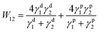 | (1) |
where superscripts d and p represent the dispersion and polar components of the surface energy. Therefore, the two components (γd and γp) of each surface are calculated by the geometric mean method:61| | (1 + cos![[thin space (1/6-em)]](https://www.rsc.org/images/entities/char_2009.gif) θt)γt = 2{(γdtγds)1/2 + (γptγps)1/2} θt)γt = 2{(γdtγds)1/2 + (γptγps)1/2} | (2) |
where θt is the contact angle of the testing droplet on the surface, γdt and γpt represent the dispersion and polar components of the testing droplet, and γds and γps represent the two calculative components of films or substrates, shown in Table 1. All the surface energies and the calculated work of adhesion are shown in Table 2. Because the glass substrate without any treatment has a negative T value (WPDMS/SY–WSY/glass < 0), the SY film cannot be detached from the sacrificing substrate easily. Therefore, we used (3-methacryloxypropyl)trimethoxysilane (MPTS) self-assembled monolayer (SAM) to reduce surface energy of the glass substrate and thus satisfy a positive T value (WPDMS/SY–WSY/glass (MPTS treatment) > 0) combined with the formation of the smooth and uniform film. Once the PDMS stamp with SY atop was conformably brought into contact with the SC-HTL, it is obvious that the film SY tended to be printed successfully on the seeding SC-HTL due to the high T value of up to −42.7 and −41.1 mJ m−2, respectively, for the cases with mCP and DMAC-DPS. The photos and contact angles of two kinds of testing droplet including water and ethylene glycol on various surfaces are shown in Fig. 2.
Table 1 The testing droplet surface energies of water and ethylene glycol
| Testing droplet |
γ (γp + γd) (mN m−1) |
γ
d (mN m−1) |
γ
p (mN m−1) |
| Water |
26.0 |
46.8 |
72.8 |
| Ethylene glycol |
26.4 |
21.3 |
47.7 |
Table 2 Surface energies of glass with and without MPTS treatment, PDMS, SY, and two seeding layers, and the work of adhesion (W) between SY and the other surfaces, the difference of work of adhesion (T) between the PDMS/SY interface and SY/substrate or HTL interface (WPDMS/SY − WSY/substrate or HTL)
| Substrate or film |
γ (γp + γd) (mN m−1) |
γ
d (mN m−1) |
γ
p (mN m−1) |
W
SY/substrate&film (mJ m−2) |
T
|
| Glass (no treatment) |
114.1 |
1.7 |
112.4 |
14.3 |
−1.4 |
| Glass (MPTS treatment) |
60.4 |
0.2 |
60.2 |
8.9 |
4.0 |
| PDMS |
7.9 |
1.9 |
6.1 |
12.9 |
0 |
| SY |
15.7 |
13.6 |
2.1 |
— |
— |
| mCP |
382.4 |
90.7 |
291.7 |
55.6 |
−42.7 |
| DMAC-DPS |
342.5 |
71.0 |
271.5 |
54.0 |
−41.1 |
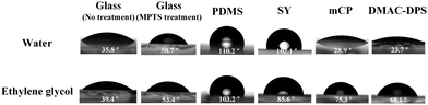 |
| | Fig. 2 The photos and contact angles of droplets including water and ethylene glycol on various surfaces. | |
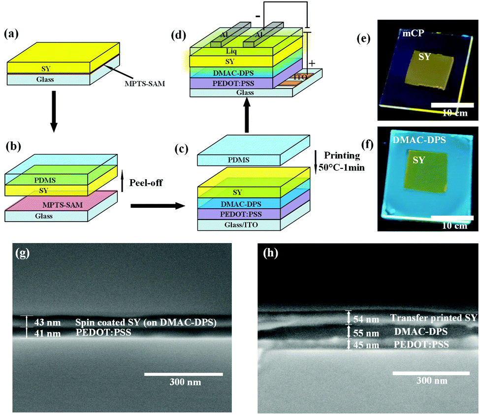
Fig. 3(a)–(d) schematically describe the preparation of the films and the EL devices. The SY suspended in chlorobenzene was spin-coated on the MPTS-treated glass and subsequently the film was stripped by PDMS. The SY film on PDMS was printed onto DMAC-DPS or mCP spin-coated directly onto poly(3,4-ethylenedioxythiophene) polystyrene sulfonate (PEDOT:PSS). To aid the detachment, a thermal treatment at 50 °C for 1 min was conducted and then the PDMS stamp was removed very carefully. The uniform SY film remained on the SC-HTL because of the satisfactory work of adhesion (see more details in Experimental section in ESI†). Fig. 3e and f illustrate the fluorescence photos of TP-SY on spin-coated mCP and DMAC-DPS, respectively. In order to verify the dissolution effect when the chlorobenzene solution with SY was spin-coated on the HTL, the SEM images of the cross-sections were taken for comparison (Fig. 3g and h). It is very obvious that the small molecular HTL was almost completely washed away by SY in chlorobenzene. In contrast, TP-SY has an intimate contact with DMAC-DPS with a distinct interface.
 |
| | Fig. 3 Schematic diagram for the transfer printing procedures and the device structure. (a) Spin-coating the EML on the MPTS-treated glass. (b) Peeling off the EML quickly from glass by using PDMS. (c) Printing the EML onto DMAC-DPS or mCP carefully followed with 50 °C heating for 1 min. (d) Liq and Al are thermally evaporated sequentially on the EML to constitute the device. Fluorescence photos of the TP-SY on (e) mCP and (f) DMAC-DPS under 365 nm UV-light. The thicknesses of these films are almost the same in the devices. Scanning electron microscopy (SEM) pictures of SC-SY (g) and TP-SY (h) on DMAC-DPS on top of PEDOT:PSS on the silicon substrates, respectively. | |
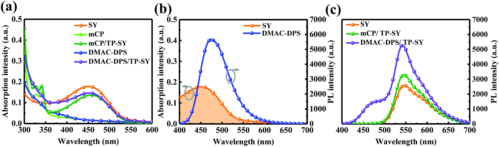
Fig. 4a shows the absorption spectra of SY, the seeding layers and TP-SY on the seeding HTLs. It is clear that the absorption spectrum of TP-SY on either seeding layer is basically the superposition of the two layers. As we can easily see, the spectral overlapping between the PL spectrum of DMAC-DPS and the absorption of SY is preferable (see Fig. 4b), which indicates the potentially effective Förster energy transfer from DMAC-DPS to SY.44 Meanwhile, Fig. 4c presents the PL spectra of SY with and without the seeding layers under 380 nm excitation. The intensity of mCP/TP-SY is slightly higher than that of neat SY. Furthermore, since SY can harvest the excitons from DMAC-DPS, the photoluminescence intensity of TP-SY is dramatically promoted compared with that of mCP/TP-SY, and thus the internal quantum efficiency is evidently enhanced.
 |
| | Fig. 4 (a) Absorption spectra of SY, mCP, DMAC-DPS, mCP/TP-SY and DMAC-DPS/TP-SY films. (b) The overlapping of the absorption of the SY film and the PL of the DMAC-DPS film. (c) PL spectra of SY, mCP/TP-SY and DMAC-DPS/TP-SY films observed from the side of SY. The thicknesses of these films are almost the same in the devices. | |
To disclose the energy transfer mechanism, the PL transient decays of SY, DMAC-DPS, mCP/TP-SY and DMAC-DPS/TP-SY are acquired in Fig. 5a and b. As we can see in Fig. 5a, in order to avoid the residual emission from DMAC-DPS, the PL transient decay curves of the films with the different seeding layers were observed at 650 nm. The PL lifetime of SY slightly increases from 2.35 ns for the neat film to 2.45 ns for mCP/TP-SY, and to 2.87 ns for DMAC-DPS/TP-SY. This means that the additional decay channels exist when utilizing mCP or DMAC-DPS as the seeding layer. Because the SY utilizes the singlet excitons from DMAC-DPS, which withstands a process of reverse intersystem crossing (RISC), the PL lifetime increases markedly. At the same time, as shown in Fig. 5b, the prompt fluorescence and delay fluorescence lifetimes of DMAC-DPS decrease respectively from 16.64 ns and 2.99 μs to 14.96 ns and 2.73 μs. Now, it is confirmed that TP-SY adjacent to DMAC-DPS can easily quench the emission of DMAC-DPS and thus harvest the singlet excitons partially via RISC of DMAC-DPS.
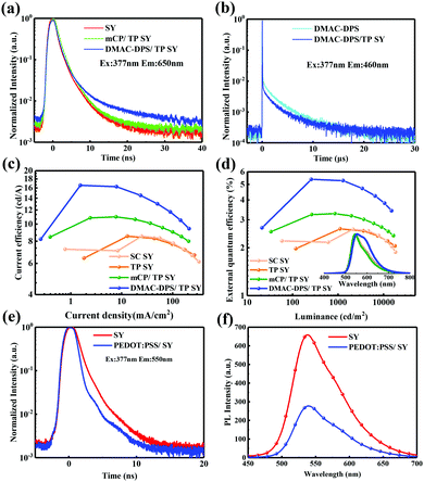 |
| | Fig. 5 (a) The PL transient decays of SY and TP-SY on the different seeding layers observed at 650 nm. (b) The PL transient decays of DMAC-DPS and DMAC-DPS/TP-SY observed at 460 nm. The thicknesses of these films are almost the same in the devices. (c) Current density–current efficiency of SY based PLED fabricated by SC and TP with the seeding HTLs. (d) Luminance–external quantum efficiency of the devices. Inset: Normalized EL spectra of the devices. The time-resolved (e) and steady-state (f) PL spectra of SY and PEDOT:PSS/SY under the same test conditions. To evidence the surface quenching effect, SY from chlorobenzene with a concentration of 0.5 mg ml−1 was spin-coated on glass and PEDOT:PSS at 1000 rpm for 30 s, respectively. | |
To evaluate the EL performances, four PLEDs were fabricated by different procedures with the configurations of ITO/PEDOT:PSS (40 nm)/none or SC-HTL (50 nm)/SY (55 nm)/8-hydroxyquinolatolithium (Liq) (1 nm)/Al (100 nm), where ITO and Al were used as the anode and cathode, PEDOT:PSS and Liq were used as the hole and electron injection layers, respectively. The corresponding EL performances are summarized in Table 3. Devices A and B denoted the ones respectively processed by SC and TP directly onto PEDOT:PSS. In comparison, devices C and D referred to the one with mCP and DMAC-DPS as the seeding HTLs, respectively. As shown in Table 3 and Fig. 5c, d, devices A and B exhibited comparable performances. The maximum EQE and CE of device D reached 5.4% and 16.6 cd A−1, respectively. It is worth noting that the efficiencies were improved by a factor of nearly 2 attributed to the introduction of the spin-coated DMAC-DPS. To better understand the performance enhancement, atomic force microscopy (AFM) was utilized to investigate the TP-SY morphology (see Fig. S2, ESI†). TP-SY on HTLs is as smooth as the SC one (RMS < 0.8 nm) which means that TP technology has no negative effects on the film morphology. Therefore, the significant improvements in the EL performances result from the following factors: (i) for SY, the hole mobility is typically larger than electron mobility.63 The additional holes injected into SY will lead to low recombination ratio of holes and electrons. As we can see in Fig. S1 (ESI†), the current density of the device with a HTL is reduced, which is ascribed to the reduced holes injected into the EML as the cathode side remains unchanged. This indeed plays a role in improving the charge balance in the EML thus leading to a higher radiative rate. Therefore, the devices with mCP and DMAC-DPS exhibit much higher EL efficiencies. (ii) DMAC-DPS donates the radiative excitons efficiently to SY which is clarified in Fig. 4, 5a and b.57,58 (iii) The exciton quenching of SY by PEDOT:PSS has been greatly alleviated,55,56,62 which can be further verified by time-resolved and steady-state PL measurements as shown in Fig. 5e and f. Both the PL lifetime and intensity are decreased once PEDOT:PSS is adjacent to SY, which indicates that the excitons generated in SY are dissipated through the non-radiative decay channels. The result profoundly proved the advantages of the SC-HTL and the TP technology exemplified in this investigation. Besides, compared with the PL spectrum of DMAC-DPS/TP SY (see Fig. 4c), there is almost no blue emission remaining in the EL spectrum (see the inset of Fig. 5d) since TP-SY almost completely quenches and then harvests the excitons from DMAC-DPS. Furthermore, as we found that with increasing driving voltages, the EL spectra of the four devices exhibit preferential spectral stability (see Fig. S3, ESI†), which basically means the fast and complete energy transfer from SC-HTL to TP-SY.
Table 3 Comparison of the EL performances
| Device |
Seeding layer |
EML |
V
10
[V] |
EQEmaxb [%] |
CEmaxb [cd A−1] |
Improvement factorc |
CIEd (x, y) |
|
The operation voltage at a luminance of 10 cd m−2.
Maximum external quantum efficiency (EQEmax), maximum current efficiency (CEmax).
Improvement factor in maximum current efficiency compared to device A.
The Commission Internationale de I'Eclairage (CIE) coordinates.
|
| A |
No |
SC-SY |
2.7 |
2.6 |
8.5 |
1.0 |
(0.42, 0.56) |
| B |
No |
TP-SY |
2.8 |
2.6 |
8.6 |
1.0 |
(0.42, 0.56) |
| C |
mCP |
TP-SY |
5.0 |
3.3 |
11.1 |
1.3 |
(0.42, 0.57) |
| D |
DMAC-DPS |
TP-SY |
6.5 |
5.4 |
16.6 |
2.0 |
(0.46, 0.52) |
Conclusions
In conclusion, we deposited a layer of transfer printed polymer on spin-coated small molecular hole transporting layers with distinct interfaces which has never been demonstrated previously without using an orthogonal solution process. This technology resulted in significant improvements in the EL performances. This combination of spin-coating and transfer printing breaks the limit of the orthogonal solvents and materials in multilayered solution processing. The TADF compound DMAC-DPS used as a hole transporting layer not only suppressed the exciton quenching by PEDOT:PSS but also resonantly transferred the excitons to the fluorescent polymer SY. An EQE of over 5% was demonstrated as well, which outperformed the limit of the traditional fluorescent devices. The interface, surface energy, and work of adhesion ruling the transfer printing process were clearly clarified. This work demonstrates the possibility and superiority of the TADF compound as the sensitizer and spin-coated HTL simultaneously, which is universal and applicable to other devices. Moreover, the seeding layer facilitates the transfer-printing technology for high-performance EL devices capable of multilayered architectures.
Conflicts of interest
There are no conflicts to declare.
Acknowledgements
This research was financially supported by the National Key Research and Development Program (2016YFB0401002), the National Natural Science Foundation of China (No. 51873159, and 61575146), the Key Technological Innovation Program of Hubei Province (No. 2018AAA013), the Natural Science Foundation of Hubei Province (No. 2017CFB687) and the Shenzhen Peacock Plan (KQTD20170330110107046). G. X. acknowledges the funding support from the Large-scale Instrument and Equipment Sharing Foundation of Wuhan University.
Notes and references
- T. Sekitani, H. Nakajima, H. Maeda, T. Fukushima, T. Aida, K. Hata and T. Someya, Nat. Mater., 2009, 8, 494–499 CrossRef CAS
 .
.
- Z. Zhang, K. Guo, Y. Li, X. Li, G. Guan, H. Li, Y. Luo, F. Zhao, Q. Zhang, B. Wei, Q. Pei and H. Peng, Nat. Photonics, 2015, 9, 233–238 CrossRef CAS .
- H. Zheng, Y. Zheng, N. Liu, N. Ai, Q. Wang, S. Wu, J. Zhou, D. Hu, S. Yu, S. Han, W. Xu, C. Luo, Y. Meng, Z. Jiang, Y. Chen, D. Li, F. Huang, J. Wang, J. Peng and Y. Cao, Nat. Commun., 2013, 4, 1971 CrossRef .
- T. Chiba, Y. J. Pu and J. Kido, Adv. Mater., 2015, 27, 4681–4687 CrossRef CAS .
- X. Yin, G. Xie, Y. Peng, B. Wang, T. Chen, S. Li, W. Zhang, L. Wang and C. Yang, Adv. Funct. Mater., 2017, 27, 1700695 CrossRef .
- B. J. De Gans, P. C. Duineveld and U. S. Schubert, Adv. Mater., 2004, 16, 203–213 CrossRef CAS .
- F. Villani, P. Vacca, G. Nenna, O. Valentino, G. Burrasca, T. Fasolino, C. Minarini and D. della Sala, J. Phys. Chem. C, 2009, 113, 13398–13402 CrossRef CAS .
- X. Liu, Z. Yu, M. Yu, X. Zhang, Y. Xu, P. Lv, S. Chu, C. Liu, W. Y. Lai and W. Huang, ACS Appl. Mater. Interfaces, 2019, 11, 26174–26184 CrossRef CAS .
- S. Chen, M. Su, C. Zhang, M. Gao, B. Bao, Q. Yang, B. Su and Y. Song, Adv. Mater., 2015, 27, 3928–3933 CrossRef CAS .
- D. Li, W. Y. Lai, Y. Z. Zhang and W. Huang, Adv. Mater., 2018, 30, 1704738 CrossRef .
- J. Zhang, Y. Zhao, Z. Wei, Y. Sun, Y. He, C.-a. Di, W. Xu, W. Hu, Y. Liu and D. Zhu, Adv. Funct. Mater., 2011, 21, 786–791 CrossRef CAS .
- Z. Lu, M. Layani, X. Zhao, L. P. Tan, T. Sun, S. Fan, Q. Yan, S. Magdassi and H. H. Hng, Small, 2014, 10, 3551–3554 CrossRef CAS PubMed .
- X. Zhang, Y. Xu, L. Fan, X. Zhang, Y. Qin, Y. Chen, J. Wang, M. Yu, W.-Y. Lai and W. Huang, Org. Electron., 2019, 75, 105380 CrossRef CAS .
- L. Zhou, M. Yu, X. Chen, S. Nie, W.-Y. Lai, W. Su, Z. Cui and W. Huang, Adv. Funct. Mater., 2018, 28, 1705955 CrossRef .
- F. Guo, A. Karl, Q. F. Xue, K. C. Tam, K. Forberich and C. J. Brabec, Light: Sci. Appl., 2017, 6, e17094 CrossRef CAS .
- C. Zhong, C. Duan, F. Huang, H. Wu and Y. Cao, Chem. Mater., 2011, 23, 326–340 CrossRef CAS .
- S. J. Cha, S. N. Cho, W. H. Lee, H. S. Chung, I. N. Kang and M. C. Suh, Macromol. Rapid Commun., 2014, 35, 807–812 CrossRef CAS .
- N. Rehmann, C. Ulbricht, A. Köhnen, P. Zacharias, M. C. Gather, D. Hertel, E. Holder, K. Meerholz and U. S. Schubert, Adv. Mater., 2008, 20, 129–133 CrossRef CAS .
- G. Liaptsis, D. Hertel and K. Meerholz, Angew. Chem., Int. Ed., 2013, 52, 9563–9567 CrossRef CAS .
- J. Park, C. Lee, J. Jung, H. Kang, K.-H. Kim, B. Ma and B. J. Kim, Adv. Funct. Mater., 2014, 24, 7588–7596 CrossRef CAS .
- M. Bender, K. M. Schelkle, N. Jürgensen, S. Schmid, G. Hernandez-Sosa and U. H. F. Bunz, Macromolecules, 2016, 49, 2957–2961 CrossRef CAS .
- K. S. Yook, S. E. Jang, S. O. Jeon and J. Y. Lee, Adv. Mater., 2010, 22, 4479–4483 CrossRef CAS .
- N. Aizawa, Y. J. Pu, M. Watanabe, T. Chiba, K. Ideta, N. Toyota, M. Igarashi, Y. Suzuri, H. Sasabe and J. Kido, Nat. Commun., 2014, 5, 5756 CrossRef .
- X. Ban, A. Zhu, T. Zhang, Z. Tong, W. Jiang and Y. Sun, ACS Appl. Mater. Interfaces, 2017, 9, 21900–21908 CrossRef CAS .
- K. Matsuoka, K. Albrecht, A. Nakayama, K. Yamamoto and K. Fujita, ACS Appl. Mater. Interfaces, 2018, 10, 33343–33352 CrossRef CAS .
- K. Albrecht, K. Matsuoka, D. Yokoyama, Y. Sakai, A. Nakayama, K. Fujita and K. Yamamoto, Chem. Commun., 2017, 53, 2439–2442 RSC .
- X. Niu, C. Qin, B. Zhang, J. Yang, Z. Xie, Y. Cheng and L. Wang, Appl. Phys. Lett., 2007, 90, 203513 CrossRef .
- S. Sax, N. Rugen-Penkalla, A. Neuhold, S. Schuh, E. Zojer, E. J. List and K. Mullen, Adv. Mater., 2010, 22, 2087–2091 CrossRef CAS .
- F. Huang, P.-I. Shih, C.-F. Shu, Y. Chi and A. K. Y. Jen, Adv. Mater., 2009, 21, 361–365 CrossRef CAS .
- Y. Zhou, T. M. Khan, J. W. Shim, A. Dindar, C. Fuentes-Hernandez and B. Kippelen, J. Mater. Chem. A, 2014, 2, 3492–3497 RSC .
- D. H. Wang, D. G. Choi, K. J. Lee, O. O. Park and J. H. Park, Langmuir, 2010, 26, 9584–9588 CrossRef CAS .
- J. B. Kim, Z.-L. Guan, S. Lee, E. Pavlopoulou, M. F. Toney, A. Kahn and Y.-L. Loo, Org. Electron., 2011, 12, 1963–1972 CrossRef CAS .
- J. K. Kim, W. Kim, D. H. Wang, H. Lee, S. M. Cho, D. G. Choi and J. H. Park, Langmuir, 2013, 29, 5377–5382 CrossRef CAS .
- F.-C. Chen, M.-K. Chuang, S.-C. Chien, J.-H. Fang and C.-W. Chu, J. Mater. Chem., 2011, 21, 11378–11382 RSC .
- H. Wang, E. D. Gomez, J. Kim, Z. Guan, C. Jaye, D. A. Fischer, A. Kahn and Y.-L. Loo, Chem. Mater., 2011, 23, 2020–2023 CrossRef CAS .
- K.-H. Yim, Z. Zheng, Z. Liang, R. H. Friend, W. T. S. Huck and J.-S. Kim, Adv. Funct. Mater., 2008, 18, 1012–1019 CrossRef CAS .
- C. W. Joo, S. O. Jeon, K. S. Yook and J. Y. Lee, Org. Electron., 2009, 10, 372–375 CrossRef CAS .
- S. O. Jeon, C. W. Joo, K. Yook and J. Y. Lee, Appl. Phys. Lett., 2009, 94, 66 Search PubMed .
- K. S. Yook, C. W. Joo, S. O. Jeon and J. Y. Lee, Org. Electron., 2010, 11, 184–187 CrossRef CAS .
- T. H. Park, Y. W. Park, J. H. Choi, H. J. Choi, J.-W. Jeong, E. H. Song, K. C. Choi and B.-K. Ju, Org. Electron., 2011, 12, 1063–1067 CrossRef CAS .
- L. A. Kim, P. O. Anikeeva, S. A. Coe-Sullivan, J. S. Steckel, M. G. Bawendi and V. Bulovic, Nano Lett., 2008, 8, 4513–4517 CrossRef CAS .
- Z. Yang, Z. Mao, Z. Xie, Y. Zhang, S. Liu, J. Zhao, J. Xu, Z. Chi and M. P. Aldred, Chem. Soc. Rev., 2017, 46, 915–1016 RSC .
- Y. Zou, S. Gong, G. Xie and C. Yang, Adv. Opt. Mater., 2018, 6, 1800568 CrossRef .
- H. Nakanotani, T. Higuchi, T. Furukawa, K. Masui, K. Morimoto, M. Numata, H. Tanaka, Y. Sagara, T. Yasuda and C. Adachi, Nat. Commun., 2014, 5, 4016 CrossRef CAS .
- D. Zhang, L. Duan, C. Li, Y. Li, H. Li, D. Zhang and Y. Qiu, Adv. Mater., 2014, 26, 5050–5055 CrossRef CAS .
- T. Furukawa, H. Nakanotani, M. Inoue and C. Adachi, Sci. Rep., 2015, 5, 8429 CrossRef CAS .
- I. H. Lee, W. Song, J. Y. Lee and S.-H. Hwang, J. Mater. Chem. C, 2015, 3, 8834–8838 RSC .
- D. Chen, X. Cai, X.-L. Li, Z. He, C. Cai, D. Chen and S.-J. Su, J. Mater. Chem. C, 2017, 5, 5223–5231 RSC .
- D. Zhang, X. Song, M. Cai and L. Duan, Adv. Mater., 2018, 30, 1707590 CrossRef .
- S. H. Han and J. Y. Lee, J. Mater. Chem. C, 2018, 6, 1504–1508 RSC .
- S. T. Levy and S. Speiser, J. Chem. Phys., 1992, 96, 3585–3593 CrossRef CAS .
- S. K. Jeon, H. J. Park and J. Y. Lee, ACS Appl. Mater. Interfaces, 2018, 10, 5700–5705 CrossRef CAS PubMed .
- N. Aizawa, S. Shikita and T. Yasuda, Chem. Mater., 2017, 29, 7014–7022 CrossRef CAS .
- Q. Zhang, B. Li, S. Huang, H. Nomura, H. Tanaka and C. Adachi, Nat. Photonics, 2014, 8, 326–332 CrossRef CAS .
- D. Abbaszadeh, G. Wetzelaer, H. T. Nicolai and P. W. Blom, J. Appl. Phys., 2014, 116, 224508 CrossRef .
- A. van Dijken, A. Perro, E. A. Meulenkamp and K. Brunner, Org. Electron., 2003, 4, 131–141 CrossRef CAS .
- B. Zhao, T. Zhang, W. Li, Z. Su, B. Chu, X. Yan, F. Jin, Y. Gao and H. Wu, Org. Electron., 2015, 23, 208–212 CrossRef CAS .
- T. Higuchi, H. Nakanotani and C. Adachi, Adv. Mater., 2015, 27, 2019–2023 CrossRef CAS .
- K. Wu, Z. Wang, L. Zhan, C. Zhong, S. Gong, G. Xie and C. Yang, J. Phys. Chem. Lett., 2018, 9, 1547–1553 CrossRef CAS .
- S. Wu, J. Polym. Sci., Part C: Polym. Symp., 1971, 34, 19–30 CrossRef .
- D. K. Owens and R. Wendt, J. Appl. Polym. Sci., 1969, 13, 1741–1747 CrossRef CAS .
- S. Nau, N. Schulte, S. Winkler, J. Frisch, A. Vollmer, N. Koch, S. Sax and E. J. List, Adv. Mater., 2013, 25, 4420–4424 CrossRef CAS .
- S. R. Tseng, Y. S. Chen, H. F. Meng, H. C. Lai, C. H. Yeh, S. F. Horng, H. H. Liao and C. S. Hsu, Synth. Met., 2009, 159, 137–141 CrossRef CAS .
Footnote |
| † Electronic supplementary information (ESI) available. See DOI: 10.1039/c9nh00431a |
|
| This journal is © The Royal Society of Chemistry 2020 |
Click here to see how this site uses Cookies. View our privacy policy here. 
 *a and
Chuluo
Yang
*a and
Chuluo
Yang