DOI:
10.1039/C9NH00275H
(Communication)
Nanoscale Horiz., 2020,
5, 163-170
Polarity-controllable MoS2 transistor for adjustable complementary logic inverter applications†
Received
24th April 2019
, Accepted 23rd August 2019
First published on 23rd August 2019
Abstract
In this work, we introduce a MoS2-based field effect transistor that can alternately operate either as a p-type or an n-type semiconductor in the same device. The proposed device is built with an adjustable threshold voltage (Vth), which can be varied by adding a layer of plasma-oxidized dielectric at the top gate structure. This facilitates a surplus of oxygen due to the relatively thin grown dielectric layer and the creation of negative charges in that layer instead of the usual ones of positive polarization in the bottom dielectric layer. Consequently, the Vth shifts and the top gate structure switches from the typical n-type to p-type while the n-type behaviour remains in the application of the bottom-gate voltages. The Vth can be tuned further by applying a gate pulse input at the top gate. Accordingly, we have demonstrated complementary logic inverters with adjustable device characteristics that are controllable by the polarity of charges induced in the device's oxide layer. This is a big step towards the concurrent implementation of both n-type and p-type characteristics in a single device.
New concepts
The cost of production has always been an important consideration in manufacturing semiconductor devices and circuits. In this study, the MoS2-based field effect transistor has been exhibited with the selective operation of either p-type or n-type characteristics in the same device. The Vth for device characteristics can be slightly adjusted further by applying a gate pulse input. Accordingly, complementary logic inverters with adjustable device characteristics have been demonstrated. Compared to the existing research, our device could save almost twice the process time and price of an individual device. This concept is useful and valuable for the future fabrication of advanced devices. We believe that these discoveries will not just lower the cost of production but will also revolutionize future complementary metal-oxide–semiconductor technology.
|
Monolayer transition-metal dichalcogenides (TMDs) have recently received immense research interest due to their outstanding electrical, mechanical, and optical properties for electronic device applications.1–6 Their unique features are ideal for the development of ultrathin, lightweight, flexible, and extremely rugged devices that can operate on arbitrary surfaces.7–9 Moreover, TMDs a have large on/off ratio and a relatively small sub-threshold swing, which makes them one of the most suitable options for logic-circuit applications10–12 such as a complementary metal-oxide–semiconductor (CMOS) inverter.
CMOS inverters, commonly used in digital logic circuits, are also employed in analog applications, such as amplifier stages13 and comparators.14,15 One of the comparator's main applications is the analog-to-digital converter (ADC) in which performance is evaluated based on two factors: power dissipation and speed. Flash ADC is the fastest ADC ever built so far; but despite its remarkable speed, it still exhibits large power consumption due to multiple comparators used to complete the conversion. A common way of solving this issue is to use a Threshold Inverter Quantization (TIQ) comparator,14,15 which has low power consumption due to the absence of a resistor array typically used in other comparator designs to generate the reference voltage. Note that the reference voltage of TIQ depends on the threshold voltage (Vth) of its CMOS inverter and that the inverter's gate width and length determines the value of this Vth. Therefore, if the inverter's Vth is tunable, then there is no need to design comparators with different gate dimensions. As a result, the ADC design process will be greatly simplified and the cost of production will be reduced accordingly.
Moreover, the ability to tune Vth is very important in finding out the device's optimal power consumption and performance16 but this seems hard to employ in atomically-thin TMD-based devices.17 In conventional CMOS technology, the Vth can be controlled by tuning the channel region doping level; however, general ion implantation is not suitable for TMDs because the technique can cause fatal damage to its crystal structure.18 A more feasible method to control the Vth of the TMD-based field effect transistors (FETs) was reported and it is by changing the dielectric layer on top of the channel.19–21 This change in the Vth is induced by the variation of the interface charges in the dielectric layer. One may also trigger off either a p-type or an n-type behaviour on the device depending on what type of process is used to grow the dielectric material.
A complementary logic inverter, which has both p- and n-type constituent transistors, is required not just for comparators but for most circuits in general. However, the difference in parameters between the PMOS and NMOS necessitates almost twice the processing time of an individual device. This can be resolved by building a single transistor that shows both p- and n-type behaviour. Interestingly, when SiO2 is grown by a thermal oxidation process on the channel, the positive charge state is dominant in the oxide layer,22–25 which may lead to an n-type behaviour with MoS2 channels. Meanwhile, when SiO2 is grown by a plasma oxidation process, which is a method that has a low deposition rate leading to relatively thin grown layers, a surplus of oxygen is induced in the dielectric material. This time, the negative charge state is more stable26 in the oxide layer that may result in a p-type behaviour with MoS2 channels. A similar idea about polarity change induced by dielectric materials MgO in black phosphorus has been reported.27,28 It is possible to employ the two aforementioned dielectric layer types as gate oxides on its back and top gate structures respectively, a MoS2 FET device can exhibit either an NMOS or a PMOS behaviour accordingly. Pair this with an adjustable Vth feature and the number of comparators in a circuit as well as the cost of production can be significantly reduced. In this paper, we have demonstrated a polarity-controllable MoS2-based field effect transistor that operates alternately as a PMOS (by its top gate) or an NMOS (by its back gate) and is built with an adjustable threshold voltage. The polarity of charges induced in the device's oxide layers controls the characteristics of the device, resulting in either a p-type or an n-type behaviour at its gate structures, thus the term polarity-controllable. We expect that our proposed device can usher in more practical and breakthrough applications in future CMOS technology.
In this study, a double gate V-shaped MoS2 field effect transistor with 12 nm length (L) and 100 nm width (W) was fabricated as illustrated in Fig. 1(a). Notice the two gates that are located at the top (top gate) and at the bottom (back gate) of the device. The optical microscope image of the actual device with the top gate, as well as an inset showing its scanning electron microscope image of the MoS2 grown along with the electrodes without the top gate, are displayed in Fig. 1(b). Details about the fabrication of the MoS2 device are reported in our previous work.29 The material characterization such as Raman, photoluminescence spectrum and transmission electron microscope images are displayed in Fig. S1 (ESI†), indicating that the uniformity is smooth with a thickness around 5 nm in a multilayer formation. In order to identify the influence of the dielectric layer to the device characteristics, two kinds of samples were built – the proposed device and a reference device. The reference device (Fig. 1(c)) has its MoS2 sheet capped with a 10 nm HfO2 dielectric layer as the top gate. On the other hand, the proposed device (Fig. 1(d)) has a 5 nm SiO2 layer grown using a plasma oxidation process on the MoS2 sheet before getting capped by a 10 nm HfO2 top gate layer. The SiO2 near the back gate of both kinds of samples is developed using the thermal oxidation process.
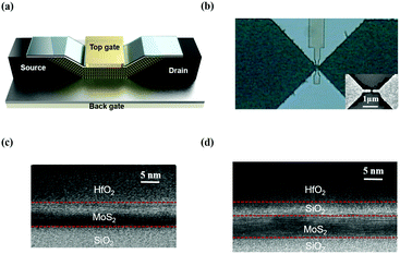 |
| | Fig. 1 The schematic diagram and characterization of the double gate MoS2 field effect transistor structure. (a) The schematic plot of the double gate MoS2 field effect transistor in which the yellow ribbons are the MoS2 layers grown in between two poly-Si electrodes (black-shaded areas); and top gate metals are deposited using TaN/TiN. (b) The top view of the optical micrograph of the double gate device. The inset shows the corresponding scanning electron microscope image of the bottom gate device (before fabricating the top gate structure). (c) and (d) are the cross-sectional images of the transmission electron microscope images showing the thickness of the MoS2 and the dielectric layers in the reference and proposed device, respectively. | |
The measurement setup is shown in Fig. 2(a) and the transfer curve in the back gate device before fabricating the top gate structure is shown in Fig. 2(b). The mobility of the back gate MoS2 FET is estimated to be about 1.2 × 10⁻² cm2 V−1 s−1. After fabricating the top gate structure, both the proposed and the reference devices exhibit an n-type behaviour when the gate voltage was applied on the back gate (back gate operation). However, the proposed device, which has a plasma-oxidized SiO2 dielectric layer in between MoS2 and HfO2, showed a p-type behaviour when the gate voltage was applied on the top gate (top gate operation). This is in contrast with the reference device, which still exhibits an n-type behaviour regardless of which gate is used in the measurement. This phenomenon in the proposed device can distinguishingly be seen in Fig. 2(c) and (d), in which the related mobilities are separately calculated to be 1.05 × 10⁻⁵ cm2 V−1 s−1 and 3.2 × 10⁻² cm2 V−1 s−1, along with the other important features of bias voltage dependence presented in Fig. S2 (ESI†). Therefore, the proposed device can alternately operate as an n-type, by using its back gate, or a p-type, by using its top gate as a gate terminal. This can also be observed in its transfer curves (Fig. 2(e)), in which the related mobilities are respectively calculated to be 6.4 × 10⁻³ cm2 V−1 s−1 by back gate operation and 3.89 × 10⁻³ cm2 V−1 s−1 by top gate operation. Similar behaviour in another device is shown in Fig. S3 (ESI†) and the general leakage current during the measurement in the proposed devices is a few pA as also shown in Fig. S4 (ESI†). It is noted that the mobility and current density are dramatically decreased as one compares between before and after directly depositing HfO2 on MoS2 (Fig. 2(b) and (c)). With the information on the transfer curves in the operation of the back gate before and after top gate process, as shown in Fig. S5 (ESI†), we can eliminate contact contribution and conclude that the low current level and low mobility are mainly caused by the damage of directly depositing dielectric materials on top of MoS2 by plasma collision.
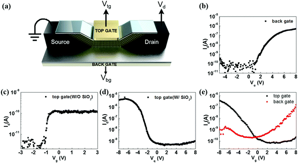 |
| | Fig. 2 Electrical characterization of double gate MoS2 field effect transistor. (a) The measurement setup. (b) The transfer characteristics of the device's (b) back gate structure at Vd = 2.1 V (before fabricating the top gate structure) as well as its top gate structure, (c) without SiO2 and (d) with the SiO2 layer, are shown. (e) The device top gate with the SiO2 layer shows transfer characteristics with both PMOS and NMOS behavior. | |
This behaviour – having two opposite characteristics – may be due to the difference in the dielectric oxide charges of the proposed device's top gate and the back gate structure. At no gate bias conditions in the reference device, the HfO2 dielectric layer has positive oxide charges that would induce a band down-bending (Fig. 3(a)). This down-bending would reduce the effective Schottky barrier between the contact metal electrode and MoS2, thus electrons are transported easily across the metal and conduction band through a thermal-assisted tunneling process (Fig. 3(b)).20,30 On the other hand, at no gate bias condition in the proposed device, the negative oxide charges formed in the plasma SiO2 dielectric layer caused the energy band in the MoS2 interface to bend up (Fig. 3(c)). This led to a decrease in the electron current since the effective Schottky barrier height for electrons was enlarged; and, at the same time, it caused an increase in the hole current, due to a reduction of the effective Schottky barrier height for holes. As a result, the Fermi level of MoS2 was effectively decreased (Fig. 3(d)). Note that once the effective Schottky barrier heights for electrons and holes become comparable at zero gate bias, the device is more likely to behave as an ambipolar transistor.20 In addition, one may notice that the proposed device's transfer characteristics demonstrate a better performance compared to the reference device due probably to the insertion of the thin SiO2 dielectric layer to prevent damage from directly depositing HfO2 on top of MoS2.
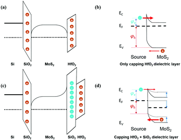 |
| | Fig. 3 Vertical and horizontal schematic energy band diagrams of the double gate MoS2 field effect transistor. (a) and (b) indicate the effect of capping the MoS2 with only an HfO2 dielectric layer, while (c) and (d) indicate the effect of capping it with both HfO2 and SiO2 dielectric layers. The band diagrams show the effective Schottky barrier heights for electrons/holes at the contact edges. | |
The proposed device's mechanism is supported by the corresponding theoretical calculations. The following assumptions were set: MoS2 doping concentration, Nd, equal to 1011 cm−2![[thin space (1/6-em)]](https://www.rsc.org/images/entities/char_2009.gif) 31,32 and band gap energy, Eg, equivalent to 1.4 eV;33 work function, ϕ′, of TaN and Si equal to 4.5 eV34 and 4.25 eV33 respectively; electron affinity, χ′, in the SiO2–MoS2 interfaces having values of 3.7 eV33 accordingly; permittivity, ε, of MoS2, SiO2, and HfO2 recorded as 11ε0,35 3.9ε0,36 and 23ε037 respectively; and the intrinsic concentration, ni equal to 1010 cm−2.38 The details of the corresponding calculations for each value are shown in the ESI.†
31,32 and band gap energy, Eg, equivalent to 1.4 eV;33 work function, ϕ′, of TaN and Si equal to 4.5 eV34 and 4.25 eV33 respectively; electron affinity, χ′, in the SiO2–MoS2 interfaces having values of 3.7 eV33 accordingly; permittivity, ε, of MoS2, SiO2, and HfO2 recorded as 11ε0,35 3.9ε0,36 and 23ε037 respectively; and the intrinsic concentration, ni equal to 1010 cm−2.38 The details of the corresponding calculations for each value are shown in the ESI.†
In general, when a positive bias is applied onto the gate terminal of the device, the work function difference, ϕms, between the metal and the semiconductor, and the threshold voltage, Vth, are given by the equations
| | | ϕms = ϕm′ − (χ′ + Eg/2e + ϕB) | (1) |
and
| | | Vth = (|QSD(max)′| − QSS′)(tox/εox) + ϕms + 2ϕB | (2) |
respectively. Here,
ϕm′ is the modified work function of the metal;
χ′ is the modified electron affinity of the semiconductor;
QSS′, is the trapped oxide charges in the dielectric layer and in its interface with the semiconductor;
tox and
εox are the thickness, and dielectric constant of the oxide layer, respectively; and
ϕB is the semiconductor potential. In the presence of two dielectric layers, such as our top gate structure,
Vth can be expressed as
| | | Vth = (|QSD′(max)|(tox1/εox1 +tox2/εox2) − QSS1′(tox1/εox1) − QSS2′ (tox2/εox2)) + ϕms + 2ϕB | (3) |
with
QSS1′,
tox1 and
εox1 referring to the 1st dielectric layer and
QSS2′,
tox2,
εox2 for the 2nd dielectric layer. In contrast, when a negative bias is applied, the following equations take place
| | | ϕms = ϕm′ − (χ′ + Eg/2e − ϕB) | (4) |
and
| | | Vth = (−|QSD′(max)| − QSS′)(tox/εox) + ϕms − 2ϕB | (5) |
| | | Vth = (−|QSD′(max)|(tox1/εox1 + tox2/εox2) − QSS1′(tox1/εox1) − QSS2′(tox2/εox2)) + ϕms − 2ϕB | (6) |
The semiconductor potential, ϕB, can be described by the relation:
where
Vt is the thermal voltage. Knowing the value of
ϕB, the maximum inversion width (
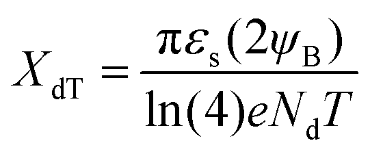
XdT) is calculated below.
39| |  | (8) |
where
T is the semiconductor thickness. We can calculate the 2D material maximum width of the depletion region,
XdT, which is about 1.62 × 10
−5 cm in our case. The charge in the depletion region at strong inversion, |
QSD′(max)|, can then be determined using the formula
which gives us a value of 6.48 × 10
−7 C cm
−2. These values will be useful in the succeeding calculations.
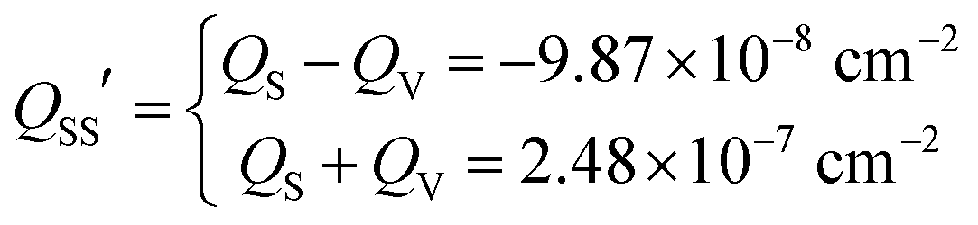
During the back gate operation, applying a positive gate bias gives a ϕms that is equal to −0.209 eV and a measured Vth of 6.4 V (Fig. 2(e)). Using eqn (2), the corresponding trapped oxide charges QSS′ is calculated to be around −9.87 × 10⁻⁸ C cm−2. Meanwhile, applying a negative bias, still on the back gate of the device, gives a ϕms that is equal to −0.091 eV. Here, considering the ambipolar characteristics of the device and in order to make the theoretical predictions closer to our experimental results, we assume a Vth of −8 V. As a result, the QSS′ is found to be around 2.48 × 10⁻⁷ C cm−2. Basically, QSS′ is composed of bias-dependent border traps-induced charges (QV) which border traps related descriptions are shown in Fig. S6 (ESI†) and bias-independent oxide charges (QS) which includes fixed oxide charges, mobile ionic charges, and oxide trapped charges to name a few. Due to the bias-dependence of QV, the relationship of QSS′ with QS and QV can be expressed using two different equations depending on the polarity of the applied gate bias, using these equations,
By solving the simultaneous equations above, QV is found to be about 7.49 × 10⁻⁸ C cm−2, while QS is about 3.46 × 10⁻⁷ C cm−2.
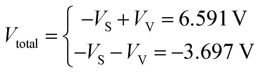
For the top gate operation, we also considered the influence of border traps in calculating the top gate dielectric layers’ charges accordingly. We assumed the quantities VV = QV1(tox1/εox1) + QV2(tox2/εox2) and VS = QS1(tox1/εox1) + QS2(tox2/εox2), in which VV is the bias-dependent voltage shift in Vth and VS is the bias-independent voltage shift in Vth. Here, VV and VS are both contributed to by the top gate structure's HfO2 (QV1 and QS1) and SiO2 (QV2 and QS2) dielectric layers. When a positive bias is applied, ϕms is 0.041 eV and, for the same reason as in the back gate operation, Vth was assumed to be 8 V; this gives a total voltage offset contribution Vtotal of 6.591 V in the HfO2–SiO2 layer. Meanwhile, in the negative bias condition, ϕms is 0.159 eV while the measured Vth is −4.8 V (Fig. 2(e)), which gives a Vtotal of −3.697 V in the HfO2–SiO2 layer. Using the equations below:
By solving the simultaneous equations above, we get VV at 5.144 V and VS equal to −1.447 V.
At no bias condition, bias-dependent QV and VV are both equal to zero. Hence, the theoretical prediction implies that, for the proposed device in such conditions, the induced oxide charges at the top gate dielectric layers is negative (QSS′ = QS) since VS is a negative sign; while the induced oxide charges at the back gate dielectric layer are positive (QSS′ = QS). Thus, the theory supports the mechanism that was discussed earlier (Fig. 3(c) and (d)). It is also important to note that, although the results from previous studies prove that HfO2 as the capping layer would induce positive oxide charges,40–42 the combination of HfO2 and plasma SiO2 still has a net negative charge. We could then infer that the negative induced charges in the plasma SiO2 layer are much greater in magnitude than the positive induced charges in HfO2. Based on the above discussion, both n-type and p-type characteristics appeared in a single device are manifestly illustrated. Accordingly, we can alternatively obtain them by operating in either the back gate or top gate through the control of the charges in which the Vth can be adjusted.
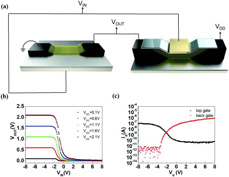
Meanwhile, from hereon we will demonstrate what the proposed device can offer for logic circuit implementations such as a CMOS inverter. In order to show our device for CMOS inverter applications, we added a separate back gate structure in another chip, which is the same with the back gate structure of the proposed device, to assist in the completion. This is necessary since our dual gate device does not have an isolation design between its two gates, which results in mixing of bias signals if both gate operations are performed at the same time in the same device. The corresponding CMOS inverter using both the top gate and the back gate structures is built as shown in Fig. 4(a). The CMOS inverter's voltage transfer characteristic (VTC) as a function of drain voltage VDD (Fig. 4(b)) clearly shows that the device guarantees either a HIGH or a LOW output voltage in the negative and positive input voltage range, respectively, provided that a given threshold value is exceeded. Moreover, as expected, the Id–Vg characteristics of both the top gate and the back gate structure at Vd = 1.1 V exhibit p-type and n-type characteristics, respectively (Fig. 4(c)). Another set of results for the same setup is presented in Fig. S7 (ESI†). With these results, we can say that, given effective isolation between its two gates, the device has the potential to operate both as a PMOS and an NMOS that could help in cutting down the number of transistors in the digital circuit.
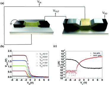 |
| | Fig. 4 Electrical characterization of MoS2 CMOS inverter device. (a) The schematic diagram showing the measurement setup using both top gate and back gate MoS2 devices that forms a CMOS inverter. (b) The voltage transfer characteristics of the CMOS inverter as a function of VDD. (c) The corresponding Id–Vg characteristic of the top gate and the back gate structure at Vd = 1.1 V. | |
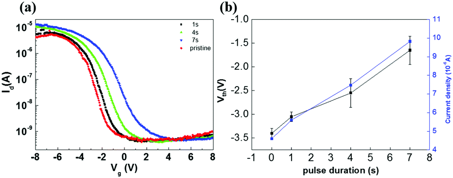
We now analyze the effect of applying a gate voltage pulse at various durations (TGS) to the electrical characteristics of the proposed device. The Id–Vg characteristics of its top gate structure as a function of TGS is shown in Fig. 5(a) with the corresponding Vth values shown in Table 1. Also, the Vthversus TGS graph of the device is presented in Fig. 5(b). Here, it is observed that when TGS lengthens, the drain current is enhanced and Vth increases. These are attributed to the long-lifetime deep electrons trapped at the MoS2/dielectric interface, formed due to the input pulses, which induced holes in the MoS2 channel.43 The longer the TGS, the more electrons get trapped and more holes are induced in the MoS2 channel. These observations can be quantitatively described using the following current and threshold voltage formula:
| | | Id = Jn × W = |QμE| × W | (10) |
| | | Vth = (−|QSD′(max)| − QSS′)(tox/εox) + ϕms − 2ϕB | (11) |
where
Jn is the current density,
W is the width of the channel,
Q is the charge per unit area at the inversion layer, and
E is the electric intensity. An increase in the number of holes corresponds to an increase in charge,
Q, that leads to an enhancement of the drain current as suggested in
eqn (10). Consequently, an increase in the number of electrons trapped at the MoS
2/dielectric interface results in a more negative
QSS′. Therefore, referring to
eqn (11), the
Vth will also increase. These are all consistent with our experimental results presented in
Fig. 5. The same results from a similar device are also shown in Fig. S8 and Table S1 (ESI
†). However, this behaviour is sensitive to the environment or charges, such as static electricity from probing and also it is not obvious in the back gate structure probably because the top gate dielectric layers are thin enough to easily cause changes in their electrical features, in contrast to the back gate dielectric layers. These clearly show the capability of the device to easily adjust its electrical properties, such as its
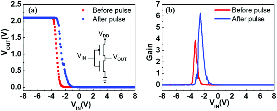
Vth, with an application of an external pulse, which is useful for several applications. For instance, for the CMOS inverters, we have demonstrated that applying a gate pulse on the top gate structure of the device does not only change its
Vth but also improves its gain. As mentioned, a change in
Vth was observed after applying a −8 V pulse at
TGS = 5 s and
Vd = 2.1 V into the top gate shown in
Fig. 6(a). This leads to an increase in the gain by 2.4 (
Fig. 6(b)). Another similar device shows the same result, which is presented in Fig. S9 (ESI
†). In order to get the ideal switching voltage and ensure the inverter fully voltage matched, the dimension for two devices (p-type and n-type) should be the same in the future design.
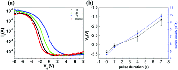 |
| | Fig. 5 Electrical characterization of the double gate MoS2 field effect transistor at different values of gate voltage pulse duration (TGS) in a fixed −8 V gate voltage pulse. (a) The Id–Vg characteristics of the top gate structure as a function of TGS. (b) The current density and Vth tendency at different values of TGS where it is observed that the longer the TGS, the greater the value of the current density and Vth. | |
Table 1 The corresponding current density at a fixed gate voltage of −6 V and Vth values in a fixed gate voltage pulse of −8 V at various duration times while the gate voltage sweeps from −8 V to 8 V
| Pulse duration |
Pristine |
1s |
4s |
7s |
| Current density (A) at −6 V |
4.6 × 10⁻⁶ |
5.6 × 10⁻⁶ |
7.48 × 10⁻⁶ |
9.82 × 10⁻⁶ |
| Threshold voltage (Vth) |
−3.4 V |
−3.05 V |
−2.55 V |
−1.65 |
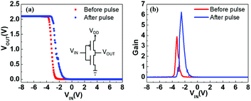 |
| | Fig. 6 Electrical characterization of the MoS2 CMOS inverter with an adjustable behavior. (a) The voltage transfer characteristics of the inverter at Vd = 2.1 V. The red and blue curves represent the measurements before and after applying a −8 V gate voltage pulse at TGS = 5 s, respectively. In the right inset is the circuit diagram of the inverter. (b) Gain characteristics of the inverter at Vd = 2.1 V showing a maxima gain value of about from 4 to 6.2, after applying the same gate voltage pulse as in (a). | |
Conclusions
We have fabricated two kinds of dual gate field effect transistors. Our proposed device showcases the importance of the oxide charges of the dielectric layer to the devices’ electrical characteristics. The result we have found is that the proposed device can alternately exhibit either an n-type or a p-type behaviour. The outcome of our findings suggests that the device can function as a CMOS inverter, and by applying a gate pulse input to the top gate, it demonstrates the attributes of its threshold voltage shift and gain enhancement. Given the effective isolation mechanism, the proposed device can both operate as a PMOS and an NMOS. Moreover, due to the adjustability of its threshold voltage, the number of comparators required to operate for ADC could be reduced, hence essentially lowering the cost of various digital circuit applications. Based on the result of our experiments, it can also serve as a foundation for further research regarding practical applications.
Methods/experimental
Device fabrication
A 30 nm bottom gate SiO2 dielectric layer was grown by thermal oxidation on a Si substrate, then, on top of it, a 200 nm poly was deposited using Low Pressure Chemical Vapor Deposition (LPCVD) at 600 °C. After plasma dry etching, a 12 nm gate length (LG) was defined by e-beam lithography. Ar gas was used to carry Sulfur and MoO3 in a hot furnace to react and deposit MoS2 onto the surface of a V-shaped Source/Drain substrate at 755 °C by a chemical vapor deposition (CVD) process, which could provide outstanding channel coverage. The key to controlling the MoS2 on the channel position is to pre-pattern two electrodes with the separation of below 1 micrometer, which could probably provide a lower surface energy for MoS2 nucleation. After MoS2 deposition, the first (reference) sample was capped with a 10 nm HfO2 as the top gate dielectric layer, while the second (proposed) one was covered with a 5 nm SiO2 by a plasma oxidation process followed by a 10 nm HfO2 as top gate dielectric materials. Finally, TaN/TiN (High-K Metal Gate) were deposited on top of the dielectric material/s by plasma-enhanced atomic layer deposition (PEALD).
Electrical characterization of devices
All the electrical properties of the fabricated devices were measured using a semiconductor parameter analyzer (Keithley 4200) at room temperature.
Conflicts of interest
The authors declare no competing financial interests.
Acknowledgements
This work were supported by the Ministry of Science and Technology, Taiwan under contract No. MOST 105-2112-M-003-016-MY3, 108-2112-M-003-010-MY3 and 108-2221-E-492-013 and was in part supported by the National Nano Device Laboratories.
References
- A. C. Ferrari, F. Bonaccorso, V. Fal'ko, K. S. Novoselov, S. Roche, P. Bøggild, S. Borini, F. H. Koppens, V. Palermo, N. Pugno, J. A. Garrido, R. Sordan, A. Bianco, L. Ballerini, M. Prato, E. Lidorikis, J. Kivioja, C. Marinelli, T. Ryhänen, A. Morpurgo, J. N. Coleman, V. Nicolosi, L. Colombo, A. Fert, M. Garcia-Hernandez, A. Bachtold, G. F. Schneider, F. Guinea, C. Dekker, M. Barbone, Z. Sun, C. Galiotis, A. N. Grigorenko, G. Konstantatos, A. Kis, M. Katsnelson, L. Vandersypen, A. Loiseau, V. Morandi, D. Neumaier, E. Treossi, V. Pellegrini, M. Polini, A. Tredicucci, G. M. Williams, B. H. Hong, J. H. Ahn, J. M. Kim, H. Zirath, B. J. van Wees, H. van der Zant, L. Occhipinti, A. Di Matteo, I. A. Kinloch, T. Seyller, E. Quesnel, X. Feng, K. Teo, N. Rupesinghe, P. Hakonen, S. R. Neil, Q. Tannock, T. Löfwander and J. Kinaret, Science and technology roadmap for graphene, related two-dimensional crystals, and hybrid systems, Nanoscale, 2015, 7, 4598 RSC.
- K. S. Novoselov, D. Jiang, F. Schedin, T. J. Booth, V. V. Khotkevich, S. V. Morozov and A. K. Geim, Two-dimensional atomic crystals, Proc. Natl. Acad. Sci. U. S. A., 2005, 102, 10451–10453 CrossRef CAS.
- G. Fiori, F. Bonaccorso, G. Iannaccone, T. Palacios, D. Neumaier, A. Seabaugh, S. K. Banerjee and L. Colombo, Electronics based on two-dimensional materials, Nat. Nanotechnol., 2014, 9, 768–779 CrossRef CAS.
- Q. H. Wang, K. Kalantar-Zadeh, A. Kis, J. N. Coleman and M. S. Strano, Electronics and optoelectronics of two-dimensional transition metal dichalcogenides, Nat. Nanotechnol., 2012, 7, 699–712 CrossRef CAS PubMed.
- A. Hsu, H. Wang, Y. C. Shin, B. Mailly, X. Zhang, L. Yu, Y. Shi, Y. H. Lee, M. Dubey, K. K. Kim, J. Kong and T. Palacios, Large-area 2-D electronics: Materials, technology, and devices, Proc. IEEE, 2013, 101, 1638–1652 CAS.
- B. Radisavljevic, A. Radenovic, J. Brivio, V. Giacometti and A. Kis, Single-layer MoS2 transistors, Nat. Nanotechnol., 2011, 6, 147–150 CrossRef CAS.
- A. Reina, H. Son, L. Jiao, B. Fan, M. S. Dresselhaus, Z. Liu and J. Kong, Transferring and Identification of Single- and Few-Layer Graphene on Arbitrary Substrates, J. Phys. Chem. C, 2008, 112(46), 17741–17744 CrossRef CAS.
- D. Akinwande, N. Petrone and J. Hone, Two-dimensional flexible nanoelectronics, Nat. Commun., 2014, 5, 5678 CrossRef CAS.
- G. Shin, M. Y. Bae, H. J. Lee, S. K. Hong, C. H. Yoon, G. Zi, J. A. Rogers and J. S. Ha, SnO2 Nanowire Logic Devices on Deformable Nonplanar Substrates, ACS Nano, 2011, 5, 10009–10016 CrossRef CAS.
- H. Wang, L. Yu, Y.-H. Lee, Y. Shi, A. Hsu, M. L. Chin, L.-J. Li, M. Dubey, J. Kong and T. Palacios, Integrated circuits based on bilayer MoS2 transistors, Nano Lett., 2012, 12, 4674–4680 CrossRef CAS.
- B. Radisavljevic, M. B. Whitwick and A. Kis, Integrated Circuits and Logic Operations Based on Single Layer MoS2, ACS Nano, 2011, 5, 9934–9938 CrossRef CAS.
- A. Sanne, R. Ghosh, A. Rai, M. N. Yogeesh, S. H. Shin, A. Sharma, K. Jarvis, L. Mathew, R. Rao, D. Akinwande and S. Banerjee, Radio Frequency Transistors and Circuits Based on CVD MoS2, Nano Lett., 2015, 15, 5039–5045 CrossRef CAS.
- Z. Wang, Fully adjustable CMOS current window comparator, Microelectron. J., 1991, 22(5–6), 85–88 CrossRef.
- A. Tangel and K. Choi, “The CMOS Inverter” as a Comparator in ADC Designs, Analog Integrated Circuits and Signal Processing, 2004, 39, 147–155 CrossRef.
- O. Aytar and A. Tangel, Employing threshold inverter quantization (TIQ) technique in designing 9-Bit folding and interpolation CMOS analog-to-digital converters (ADC), Sci. Res. Essays, 2011, 6(2), 351–362 Search PubMed.
- A. P. Chandrakasan and R. W. Brodersen, Minimizing power consumption in digital CMOS circuits, Proc. IEEE, 1995, 83(4), 498–523 CrossRef.
- D. H. Kang, J. Shim, S. K. Jang, J. Jeon, M. H. Jeon, G. Y. Yeom, W. S. Jung, Y. H. Jang, S. Lee and J. H. Park, Controllable nondegenerate p-type doping of tungsten diselenide by octadecyltrichlorosilane, ACS Nano, 2015, 9(2), 1099–1107 CrossRef CAS.
- H. Y. Park, S. R. Dugasani, D. H. Kang, J. Jeon, S. K. Jang, S. Lee, Y. Roh, S. H. Park and J. H. Park, n-and p-type doping phenomenon by artificial DNA and M-DNA on two-dimensional transition metal dichalcogenides, ACS Nano, 2014, 8(11), 11603–11613 CrossRef CAS.
- J. Na, M. K. Joo, M. Shin, J. Huh, J. S. Kim, M. Piao, J. E. Jin, H. K. Jang, H. K. Jang, H. J. Choi, J. H. Shim and G. T. Kim, Low-frequency noise in multilayer MoS2 field-effect transistors: The effect of high-k passivation, Nanoscale, 2014, 6, 433–441 RSC.
- H. Liu, A. T. Neal, M. Si, Y. Du and P. D. Ye, The effect of dielectric capping on few-layer phosphorene transistors: Tuning the Schottky barrier heights, IEEE Electron Device Lett., 2014, 35(7), 795–797 CAS.
- C. Lau, T. Srimani, M. D. Bishop, G. Hills and M. M. Shulaker, Tunable n-Type Doping of Carbon Nanotubes through Engineered Atomic Layer Deposition HfOX Films, ACS Nano, 2018, 12(11), 10924–10931 CrossRef CAS.
- S. Ogawa and N. Shiono, Generalized diffusion-reaction model for the low-field charge-buildup instability at the Si–SiO2 interface, Phys. Rev. B: Condens. Matter Mater. Phys., 1995, 51(7), 4218–4230 CrossRef CAS.
- S. Chakravarthi, A. T. Krishnan, V. Reddy, C. F. Machala and S. Krishnan, A comprehensive framework for predictive modeling of negative bias temperature instability, IEEE International Reliability Physics Symposium. Proceedings, 2004, 273–282 CAS.
- M. A. Alam, H. Kufluoglu, D. Varghese and S. Mahapatra, A comprehensive model for pMOS NBTI degradation: Recent progress, Microelectron. Reliab., 2007, 47(6), 853–862 CrossRef.
- L. Tsetseris, X. J. Zhou, D. M. Fleetwood, R. D. Shrimpf and S. T. Pantelides, Physical mechanisms of negative-bias temperature instability, Appl. Phys. Lett., 2005, 86(14), 142103 CrossRef.
- A. Boogaard, A. Y. Kovalgin and R. A. M. Wolters, Negative Charge in Plasma Oxidized SiO2 Layers, ECS Trans., 2011, 35(4), 259–272 CAS.
- L. Wang, W. Liao, S. Xu, X. Gong, C. Zhu and K.-W. Ang, Unipolar n-Type Conduction in Black Phosphorus Induced by Atomic Layer Deposited MgO, IEEE Electron Device Lett., 2019, 40(3), 471–474 CAS.
- W. Liao, L. Wang, L. Chen, W. Wei, Z. Zeng, X. Feng, L. Huang, W. C. Tan, X. Huang, K. W. Ang and C. Zhu, Efficient and reliable surface charge transfer doping of black phosphorus via atomic layer deposited MgO toward high performance complementary circuits, Nanoscale, 2018, 10(36), 17007–17014 RSC.
-
K.-S. Li, B.-W. Wu, L.-J. Li, M.-Y. Li, C.-C. K. Cheng, C.-L. Hsu, C.-H. Lin, Y.-J. Chen, C.-C. Chen, C.-T. Wu, M.-C. Chen, J.-M. Shieh, W.-K. Yeh, Y.-L. Chueh, F.-L. Yang and C. Hu, MoS2 U-shape MOSFET with 10 nm channel length and poly-Si source/drain serving as seed for full wafer CVD MoS2 availability, IEEE Symposium on VLSI Technology, 2016, pp. 1–2, DOI:10.1109/vlsit.2016.7573375.
- J. Park, D. H. Kang, J. K. Kim, J. H. Park and H. Y. Yu, Efficient Threshold Voltage Adjustment Technique by Dielectric Capping Effect on MoS2 Field-Effect Transistor, IEEE Electron Device Lett., 2017, 38(8), 1172–1175 CAS.
- A. Nipane, D. Karmakar, N. Kaushik, S. Karande and S. Lodha, Few-Layer MoS2 p-Type Devices Enabled by Selective Doping Using Low Energy Phosphorus Implantation, ACS Nano, 2016, 10, 2128–2137 CrossRef CAS.
- H.-Y. Park, M.-H. Lim, J. Jeon, G. Yoo, D. H. Kang, S. K. Jang, M. H. Jeon, Y. Lee, J. H. Cho, G. Y. Yeom, W.-S. Jung, J. Lee, S. Park, S. Lee and J.-H. Park, Wide-Range Controllable n-Doping of Molybdenum Disulfide (MoS2) through Thermal and Optical Activation, ACS Nano, 2015, 9, 2368–2376 CrossRef CAS.
- V. V. Afanas’ev, D. Chiappe, C. Huyghebaert, I. Radu, S. De Gendt, M. Houssa and A. Stesmans, Band alignment at interfaces of few-monolayer MoS2 with SiO2 and HfO2, Microelectron. Eng., 2015, 147, 294–297 CrossRef.
- K. Choi, H. N. Alshareef, H. C. Wen, H. Harris, H. Luan, Y. Senzaki, P. Lysaght, P. Majhi and B. H. Lee, Effective work function modification of atomic-layer-deposited-TaN film by capping layer, Appl. Phys. Lett., 2006, 89, 032113 CrossRef.
- S. L. Howell, D. Jariwala, C. C. Wu, K. S. Chen, V. K. Sangwan, J. Kang, T. J. Marks, M. C. Hersam and L. J. Lauhon, Investigation of Band-Offsets at Monolayer-Multilayer MoS2 Junctions by Scanning Photocurrent Microscopy, Nano Lett., 2015, 15(4), 2278–2284 CrossRef CAS.
- Virginia Semiconductor, The General Properties of Si, Ge, SiGe, SiO2 and Si3N4, June 2002.
-
K. Yamada, Extended Abstracts of the 18th Conference on Solid State Devices and Materials, Tokyo, 1986, pp. 257–260.
- C.-C. Wu, D. Jariwala, V. K. Sangwan, T. J. Marks, M. C. Hersam and L. J. Lauhon, Elucidating the Photoresponse of Ultrathin MoS2 Field-Effect Transistors by Scanning Photocurrent Microscopy, J. Phys. Chem. Lett., 2013, 4(15), 2508–2513 CrossRef CAS.
- H. Ilatikhameneh, T. Ameen, F. Chen, H. Sahasrabudhe, G. Klimeck and R. Rahman, Dramatic Impact of Dimensionality on the Electrostatics of P–N Junctions and Its Sensing and Switching Applications, IEEE, 2018, 17, 293–298 CAS.
- A. Neugroschel, G. Bersuker, R. Choi and B. H. Lee, Effect of the Interfacial SiO2 Layer in High-k HfO2 Gate Stacks on NBTI, IEEE Trans. Device Mater. Reliab., 2008, 8(1), 47–61 CAS.
- J. Kang, E.-C. Lee, K. J. Chang and Y.-G. Jin, H-related defect complexes in HfO2: A model for positive fixed charge defects, Appl. Phys. Lett., 2004, 84, 3894–3896 CrossRef CAS.
- B. Min, S. P. Devireddy, Z. Çelik-Butler, F. Wang, A. Zlotnicka, H.-H. Tseng and P. J. Tobin, Low-Frequency Noise in Submicrometer MOSFETs With HfO2, HfO2/Al2O3 and HfAlOx Gate Stacks, IEEE Trans. Electron Devices, 2004, 51(10), 1679–1687 CrossRef CAS.
- G. Gu, M. G. Kane, J. E. Doty and A. H. Firester, Electron traps and hysteresis in pentacene-based organic thin-film transistors, Appl. Phys. Lett., 2005, 87, 243512 CrossRef.
Footnote |
| † Electronic supplementary information (ESI) available. See DOI: 10.1039/c9nh00275h |
|
| This journal is © The Royal Society of Chemistry 2020 |
Click here to see how this site uses Cookies. View our privacy policy here. 
 b,
Chuan-Jie
Hong
c,
Kai-Shin
Li
*d,
Yuan-Liang
Zhong
c,
Yan-Kuin
Su
ae and
Yann-Wen
Lan
b,
Chuan-Jie
Hong
c,
Kai-Shin
Li
*d,
Yuan-Liang
Zhong
c,
Yan-Kuin
Su
ae and
Yann-Wen
Lan