
 Open Access Article
 This Open Access Article is licensed under a Creative Commons Attribution-Non Commercial 3.0 Unported Licence
Morphology dependent electrical conduction and breakdown in single TiO2 nanotubes†
Sourav Kumar
Kajli
a,
Debdutta
Ray
b and
Somnath C.
Roy
 *a
*a
aDepartment of Physics, Indian Institute of Technology Madras, Chennai, Tamilnadu 600036, India. E-mail: somnath@iitm.ac.in
bDepartment of Electrical Engineering, Indian Institute of Technology Madras, Chennai, Tamilnadu 600036, India
First published on 27th November 2020
Abstract
Understanding the electrical conduction properties of a single nanostructure is essential for gaining insight into the fundamental charge transport through 1D materials and also for exploring the collective behavior of an array of such nanostructures. TiO2 nanostructures, such as electrochemically grown nanotubes, have been widely studied in recent times for several applications. The electrolyte plays a vital role in deciding the morphology, which, in turn, governs the charge transport behavior. Here we present a comparative study of the charge transport through a single TiO2 nanotube grown by electrochemical anodization using ethylene glycol and dimethyl sulphoxide electrolytes. The individual nanotubes are assembled into nanodevices using photolithography without relying on complex and sophisticated process like electron beam lithography or focused ion beam deposition. The electric field dependent charge transport properties show Schottky emission at a lower field regime and Poole–Frenkel emission in the higher region. The temperature-dependent electrical conduction (110 K–410 K) is mediated by two thermal activation processes, attributed to shallow impurities in the low-temperature range (T < 230 K) and to the donors at deep intermediate levels at higher temperatures (T > 230 K). The activation energies for EG based nanotubes are found to be higher than those for DMSO nanotubes owing to the double wall morphology of the formed tubes. Also, the study of the electrical breakdown phenomena of these nanotubes reveals three distinct categories of collapse. ‘Model A’ type breakdown is characterized by a stepwise rise of the current up to the breakdown point and a fall to zero following a non-uniform step by step decrease, which is driven by crack formation near the electrode interface and its propagation. ‘Model B’ shows a transient rise and fall in current, leading to breakdown due to electromigration, whereas ‘Model C’ type breakdown observed in a bundle of nanotubes shows a mixed trend of ‘Model A’ and ‘Model B’. The data and analysis provide insight into the current limit through an individual nanotube or bundle of nanotubes and will be useful for designing prototype nanodevices from titania nanostructures.
Introduction
One-dimensional (1D) nanostructures such as nanowires,1 nanotubes,2 nanorods,3etc. show unique characteristics owing to a higher specific surface area and a directional charge flow. These properties make 1D nanostructures potential candidates for solar energy harvesting,2 optoelectronic devices,4 electrochemical energy conversion,5 and chemical6 and gas sensors.7 Confinement in two dimensions allows movement of a majority of carriers along an axial flow configuration which also helps in separating electron–hole pairs as and when they are generated. Most of the reported work discussed arrays or bunches of nanostructures, wherein superior properties compared to those of polycrystalline materials or thin films were observed. However, to realize the collective behavior of an array of nanostructures, investigation of the properties of a single nanostructure is necessary. It provides further depth to the applications once we understand the charge transport or current conduction through a single nanostructure. Also, it has the potential to solve the drawbacks and problems related to the efficiency or performance for a device application. It is reported that single nanostructures show promising behavior in sensing applications,8 photovoltaics,9 light emitting diodes,10 transistors,11etc.Titanium dioxide is one among the most extensively explored transition metal oxides having wide-scale applications such as in photocatalysis,12 lithium-ion batteries,13 gas sensing,14,15 photoelectrochemical water splitting,16–18 dye-sensitized solar cells,19–21 disposable biosensors,22etc. In particular, titania nanotube arrays fabricated via electrochemical anodization have been widely studied in recent times, as is evident from the reviews.23–25 Electrochemical anodization results in vertically aligned arrays of TiO2 nanotubes with varying geometrical features (length, diameter, and inter-tube separation) and surface morphologies depending on the synthesis conditions. Although electrical devices are fabricated using two-point contact at the upper and lower end of the nanotube arrays, estimating charge transport in a single nanotube becomes difficult due to impurities or debris stuck on the pores or the inter-tubular spaces and inter-wall contacts. Literature reports suggest that a few studies have been performed to identify the electrical characteristics of single TiO2 nanotubes under various conditions. Fàbrega et al.26 reported photoconduction in low resistivity TiO2 nanotubes fabricated using the DMSO electrolyte. They found that the charge carriers in these nanotubes recombine following the Hall–Shockley–Read mechanism of non-radiative recombination. Stiller et al.27 studied electrical conduction in a single TiO2 nanotube and concluded that the electrical conduction is governed by the Mott variable range hopping mechanism. They also carried out impedance spectroscopy which revealed the dominance of grain cores in deciding the impedance characteristics. Hattori et al.28 compared the electrical transport behavior of single anatase and rutile TiO2 nanotubes and showed that the charge conduction follows a metal–semiconductor–metal model with the presence of a Schottky junction. Lee et al.29 carried out electrical conductivity studies on single TiO2 nanotubes using Pt interconnections made by e-beam and ion beam assisted deposition. They found that there exist about two orders of magnitude of difference in resistance depending on the deposition technique. Recently, Brahmi et al.30 reported low-temperature n–p transition in single TiO2 nanotubes.
In the electrochemical anodization process, the morphology of the resultant nanotubes significantly depends on the electrolyte31,32 used. For example, tubes with differences in wall thickness or smooth or granular surfaces and compact or separated nanotube arrays are formed with variations in the electrolyte. Such morphological differences are likely to affect the electrical properties of individual nanotubes, which, in turn, influence the performance of the fabricated devices. So far, a comparative study on the influence of morphology on the electrical conduction/charge transport in single TiO2 nanotubes has not been carried out. In this work, we present temperature-dependent electrical conduction studies on single TiO2 nanotubes obtained by electrochemical anodization in NH4F/ethylene glycol (EGTNT) and dimethyl sulfoxide (DMSO)/HF (DMTNT) electrolytes. The use of EG and DMSO based electrolytes results in markedly different morphologies; for example, smooth and double-walled nanotubes (DWNT) in EG and rough, single-walled nanotubes (SWNT) in DMSO. Further, the aim of the study is to understand how a single TiO2 nanotube behaves under an applied bias and to what extent it is capable of withstanding the current flow. Although a majority of studies have been reported on the applications of TiO2 nanotube arrays (bundles), there are also a few reports on the use of single nanotubes for applications such as biosensors,33 gas sensors,34etc. The gas or any particular adsorbate to be sensed is adsorbed at the surface of the sensing materials. The semiconducting nature of the TiO2 nanotube ensures heating of the surface under the application of a voltage through Joule heating. Because of the higher surface to volume ratio, even a small current can result in significant heating in the nanostructure, which, in turn, can tune the adsorption of the adsorbates in a favorable way. The single nanostructure such as the TiO2 nanotube can therefore act as a low power consuming, self-heating sensor under a nominal bias. However, to further explore such applications, a thorough understanding of the charge transport and its dependence on morphology is essential.
So, we have analyzed the limit of compliance and onset of catastrophic failure (breaking of nanotubes due to Joule heating) in these individual TiO2 nanotubes. The results provide a thorough insight into the electrical behavior and breakdown and also establish a platform for future device applications involving single TiO2 nanotube devices.
Experimental
Materials and device fabrication
Electrochemical anodization was performed in a two-electrode cell consisting of a Ti foil anode and a Pt cathode. Anodization was implemented using two different electrolyte media, ethylene glycol (EG) and dimethyl sulfoxide (DMSO), to obtain nanotubes with two distinct morphologies. The EG based electrolyte comprises 0.25 wt% NH4F, 2 ml DI water, and 98 ml ethylene glycol, while for DMSO, the electrolyte comprises 2 vol% HF and 98 vol% DMSO. The anodization was accomplished under potentiostatic conditions by applying 60 V for 4 hours and 50 V for 12 hours, respectively, for EG and DMSO based electrolytes. Afterward, the Ti foil samples containing vertically grown TiO2 nanotubes were dried and annealed in a furnace at 450 °C in air for 2 hours. The crystallinity of EGTNT and DMTNT was characterized using a Rigaku smartlab X-ray diffractometer (Fig. S1 in the ESI†), and the surface morphologies of the nanotube (NT) arrays were observed using an FEI Inspect F50 scanning electron microscope (SEM). The SEM images in Fig. 1(a) and (b) show that the average pore diameters are about 104 nm and 149 nm for EGTNT and DMTNT, respectively. The diameters and wall thickness of the nanotubes were measured from the FESEM images using ImageJ software. Electrical contacts to individual nanotubes were fabricated by using photolithography, metallization, and the lift-off process. Prior to this, the anatase titania NTs were removed from the titanium substrate by ultrasonication in ethanol, and a resultant dispersion was obtained. A p-type Si wafer of size 3.5 cm × 3.5 cm was used on which a 70 nm SiO2 layer was grown as an insulator. The electrodes (5 nm Cr/35 nm Au) of sizes 100 μm × 100 μm were fabricated on the Si/SiO2 substrate by photolithography, electron beam evaporation, and the lift-off process to obtain the final patterned substrate. The TiO2 nanotubes were transferred by drop-casting 10 μl of the dispersion (TiO2 NTs in ethanol) onto the patterned Si substrate. After depositing the NTs onto the array of electrodes, a high-resolution scanning electron microscope was used to locate single NTs that formed bridges between two electrodes, and the exact location was listed with the column and row numbers of the electrodes. This process is a simple, relatively inexpensive, and faster process for the fabrication of single nanotube devices compared to other sophisticated techniques like e-beam lithography and focused ion beam. The Si wafer containing TiO2 nanotubes was annealed at 150 °C for 30 min under N2 to ensure good contact between nanotubes and electrodes and to eliminate any unwanted absorbed moisture or volatile contaminants.35,36 The individual nanotubes of EGTNT and DMTNT on Cr/Au electrode pads are displayed in Fig. 1(c) and (d). The electrical characterization of the individual nanotubes was performed by analysis of temperature-dependent J–V characteristics measured in a vacuum chamber (10−5 mbar) with two probe measurements using a Semiconductor Device Parameter Analyzer (Keysight B1500A). The data analysis and curve fitting were carried out using Origin 8.5 software.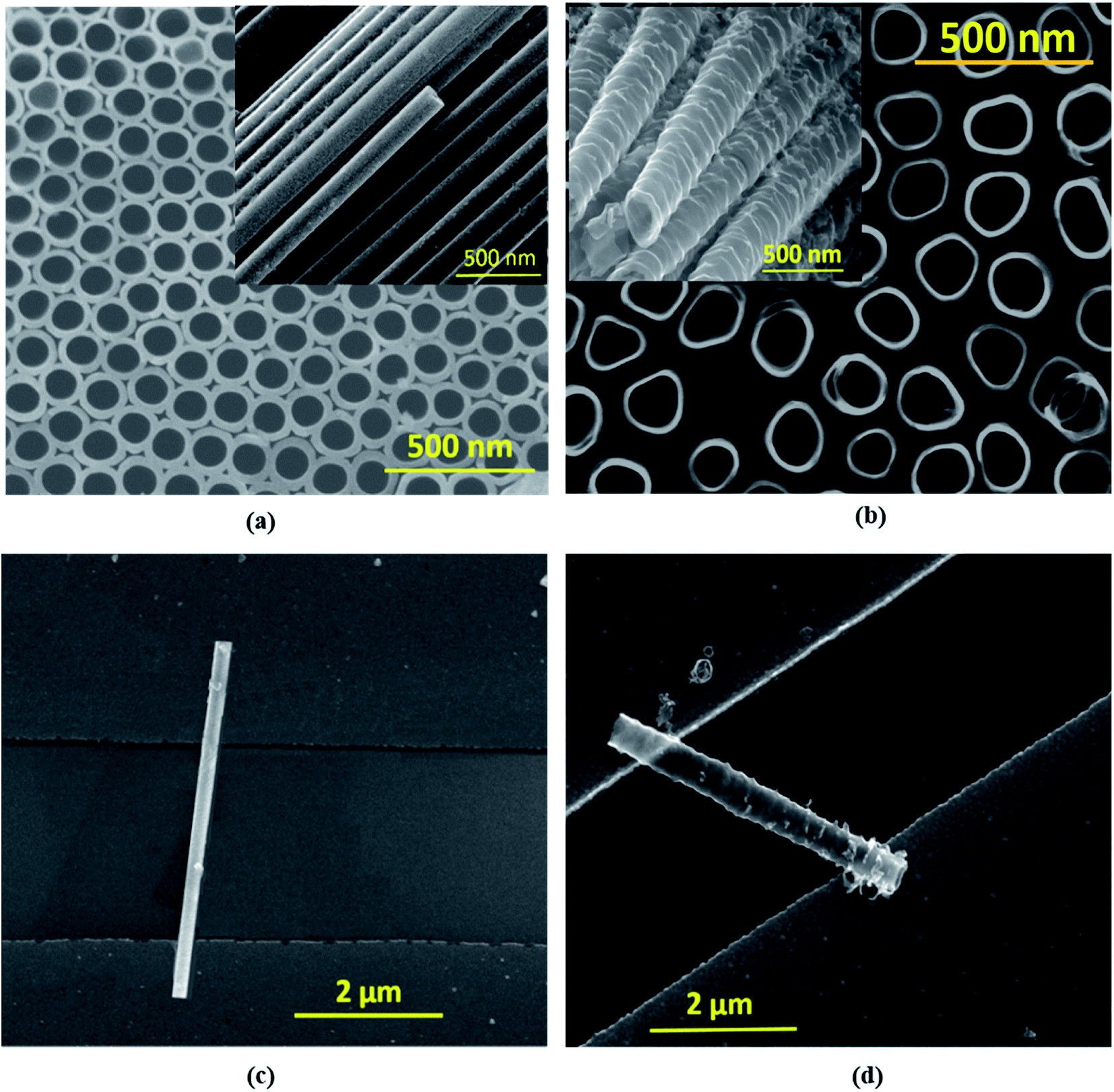 | ||
| Fig. 1 FESEM image showing the top and side view (inset) of (a) EGTNT and (b) DMTNT and (c) and (d) show the individual TiO2 nanotube devices of EGTNT and DMTNT, respectively, on Au electrodes on top of the SiO2/Si substrate. | ||
Results and discussion
Temperature-dependent and field-dependent electrical characteristics
The current density-applied bias (J–V) plots for individual EGTNT and DMTNT at room temperature are presented in Fig. 2(a). Since the conductivity of materials is governed by the carrier concentrations and mobility of the charge carriers, temperature-dependent J–V characteristics were obtained in the range of 110 K–410 K at an interval of 20 K. The data for EGTNT and DMTNT are presented in Fig. 2(b) and (c), respectively. The study shows that the current increases with temperature for both forward and reverse biases implying a typical semiconducting behavior.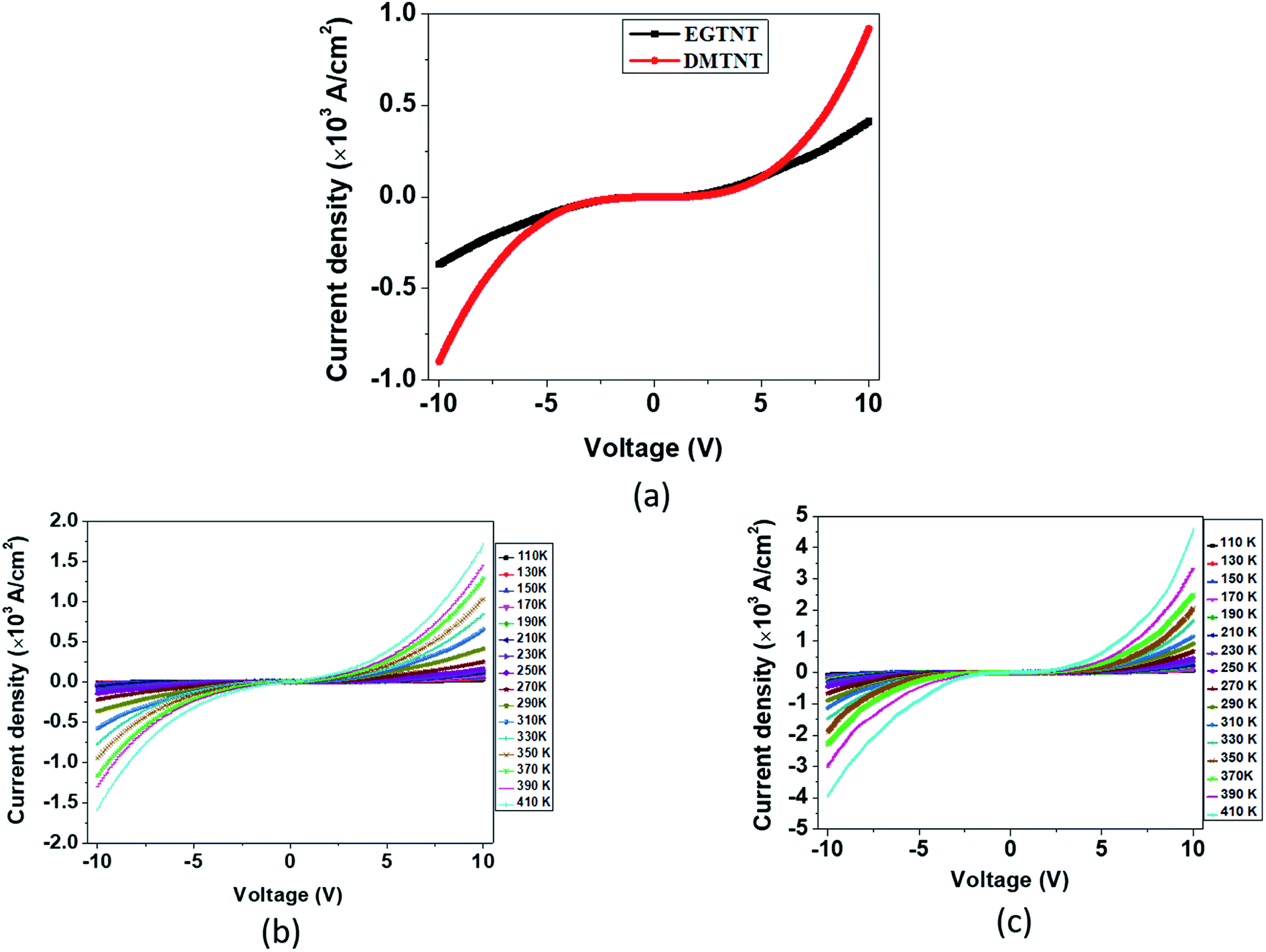 | ||
| Fig. 2 Current density–voltage (J–V) plots (a) for EGTNT and DMTNT at room temperature, (b) for the individual EGTNT at different temperatures and (c) for the individual DMTNT at different temperatures. | ||
Now, the nanotube can be considered to be a hollow cylinder, and the effective cross-sectional area can be obtained using 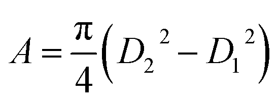 where D2 and D1 are the external and internal diameters of the nanotube, respectively. For EGTNT, the average D2 and D1 values are 151 nm and 104 nm, and for DMTNT, the average magnitudes of D2 and D1 are 188 nm and 149 nm, respectively (Fig. 1(a) and (b)), measured using ImageJ software. The approximate conductivity value (σ) can be obtained using
 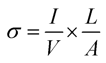 , where A and L represent the cross-sectional area and length of the nanotube, respectively. The SEM images in Fig. 1(c) and (d) show estimated effective lengths (L) of the TiO2 nanotube of about 2.61 μm and 3.02 μm for EGTNT and DMTNT, respectively, measured using ImageJ software. Therefore, the conductivity of the TiO2 nanotube, derived by assuming zero contact resistance, is given by σ ≈ 1.08 × 10⁻² S cm−1 for EGTNT and 2.77 × 10⁻² S cm−1 for DMTNT, respectively. These values are close to the reported conductivity of polycrystalline TiO2 nanotubes.37
The electrical transport in a semiconducting material can be classified into two categories: electrode limited conduction and bulk limited conduction. The electrode limited conduction mechanisms comprise Schottky or thermionic emission, Fowler–Nordheim tunneling, etc. On the other hand, the bulk limited mechanisms are Poole–Frenkel emission, hopping, space charge limited current, etc. Each of these has characteristic J–V plots with the precise nature of temperature dependence. Therefore, a thorough analysis of the J–V data at different temperatures reveals the appropriate behavior of the charge transport mechanism.
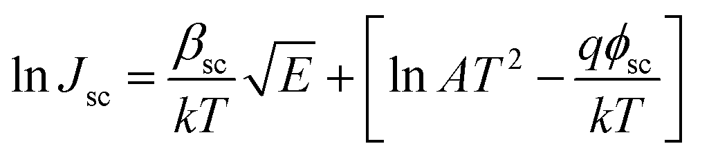
The Schottky mechanism, which is electrode limited conduction, is governed by the potential barrier (ϕsc) at the electrode semiconductor interface and influenced by both temperature (T) and electric field (E). The current density (Jsc) under the Schottky mechanism38,39 is given as
 | (1) |
 , k is the Boltzmann constant,
 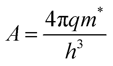 , q is the electronic charge, ε0 is the permittivity of free space, εr is the dynamic dielectric constant of the material, m* is the effective mass of electrons and h is the Planck constant. Eqn (1) helps us to calculate the barrier height at the electrode–semiconductor interface if the temperature-dependent current–voltage characteristics are known. In addition, the dynamic dielectric constant of the semiconductor can also be derived from the slope of the ln
![[thin space (1/6-em)]](https://www.rsc.org/images/entities/char_2009.gif) Jscvs. E1/2 plot.
Jscvs. E1/2 plot.
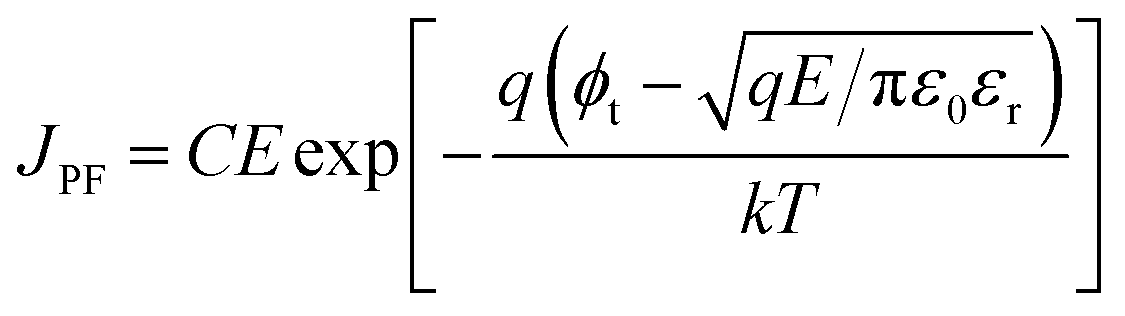
On the other hand, the bulk limited Poole–Frenkel (P–F) mechanism is governed by the movement of charge carriers from traps to the conduction band of the semiconductor by applying an electric field. A reduction in the Coulomb potential energy stimulates the release of charges from trap states, and the amount of reduction in potential energy is proportional to the probability of a charge carrier being thermally excited out of the traps. The equation relating current density JPF under P–F emission is given by
 | (2) |
Eqn (2), in particular, helps us to calculate the barrier height for the emission of charge carriers from trap states into the conduction band and also the dynamic dielectric constant of the semiconducting material from the slope of the ln(J/E) vs. E1/2 plot. To obtain a proper realization of the dominant transport mechanism,38 the current density J and J/E are plotted as a function of the square root of the electric field E in the semi-logarithmic plot, as shown in Fig. 3. The Schottky mechanism is dominant at a lower electric field, whereas the P–F mechanism is dominant at a higher field. Because of the difference in functional dependence between J and E for these two mechanisms, the slopes of the plots are characteristically different when these two mechanisms operate in different ranges of the electric field. A careful look at the data reveals that slopes of the respective curves have a “change over” at about 13000 V cm−1 for EGTNT (Fig. 3(a)) and about 16600 V cm−1 for DMTNT (Fig. 3(c)). The lower slope regions below these values are analyzed according to Schottky emission, whereas the higher slope regions greater than these values are analyzed as the P–F mechanism.
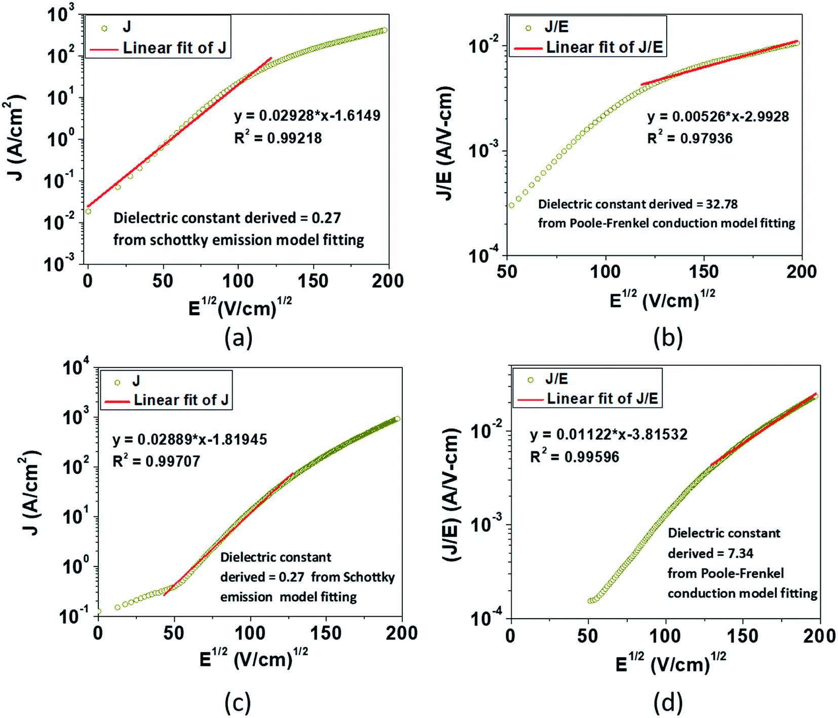 | ||
| Fig. 3 The experimental semi-logarithm plot of J vs. E1/2 according to eqn (1) for (a) EGTNT and (c) DMTNT at 290 K in the lower bias region; the experimental semi-logarithm plot of (J/E) vs. E1/2 according to eqn (2) for (b) EGTNT and (d) DMTNT at 290 K in the higher electric field area. The red straight line denotes the fitting curve to those specified equations in a fixed range of the electric field. | ||
Analysis of the data indicates that the electrical transport can be explained by a linearly fitted curve (using Origin 8.5 software) in the lower regimes of the electric field, up to approximately 13000 V cm−1 and 16600 V cm−1 for EGTNT and DMTNT, respectively, indicating the Schottky emission (illustrated in Fig. 3(a) and (c)). As the electric field increases beyond these values (approximately 15000 V cm−1 and 17000 V cm−1 for EGTNT and DMTNT, respectively), the Poole–Frenkel (P–F) mechanism dominates,40 as displayed in Fig. 3(b) and (d). Poole–Frenkel emission implies a mechanism that occurs at a high field and is similar to the Schottky emission, where charge carriers move from a trap state to the conduction band (CB) via thermal excitation and the electric field. The dielectric constant values obtained from the slope of the curves fitted to eqn (1) and (2) are tabulated in Table 1 and are the values at higher frequencies,41 not the static dielectric constant, as the electrons released from the trap state cannot polarize the surrounding medium. The magnitudes of εr are in good accord with the earlier published values of titania thin films42 and nanotubes.43,44
| Types of TiO2 nanotube | Schottky mechanism | Poole–Frenkel mechanism |
|---|---|---|
| EGTNT | 0.27 | 32.78 |
| DMTNT | 0.27 | 7.34 |
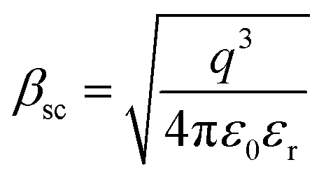
The dielectric constant values are derived from slopes 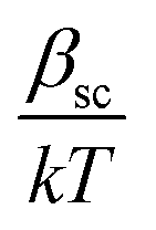 and
and 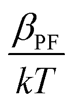 of the respective J–E plots (Fig. 3). Now keeping the temperature constant (i.e., kT is constant), in the case of the Schottky mechanism, the slope βsc is given by
 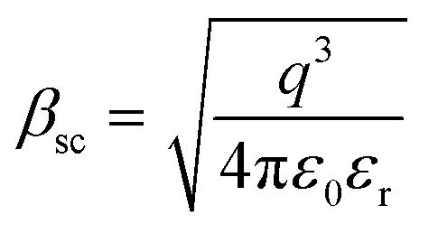 whereas for the Poole–Frenkel (P–F) mechanism, the slope βPF is given by
  .
.
Here, in both cases, the dielectric constant (εr) is inversely proportional to the square of the slope. Now, as observed in Fig. 3, the slope of the curve in the Schottky region is higher than that in the P–F region, which gives lower values of the dielectric constant derived from the Schottky mechanism compared to that from the P–F mechanism. A similar trend was also observed by Yang et al.42
The data reveal that the dielectric constant values derived from the Schottky mechanism are 0.27 for both EGTNT and DMTNT. It should be noted that the values derived from the Schottky mechanism are unrealistically low. On the other hand, the dielectric constant values derived from the P–F mechanism are 32.78 and 7.34 for EGTNT and DMTNT, respectively. The double-walled morphology of EGTNT results in additional polarization effects, and hence the dielectric constant increases. Such values are also reported by terahertz spectroscopy for EG based TiO2 nanotubes.43,44
The current density is dependent on both the concentration and mobility of the charge carriers, both of which are functions of temperature. When the current densities are plotted as a function of 1/T, the slope of the curve gives information about the activation energy, which is an important parameter for charge conduction. The current density is plotted with respect to 1/T at different voltages to ascertain if the activation energy has voltage dependence. The experimental plots of the measured current densities at different voltages (5 V, 7 V, and 10 V) with the inverse of temperature are shown in Fig. 4. The plots have two linear segments with distinct slopes corresponding to various temperature ranges of ∼110–230 K (small dotted line) and ∼230–410 K (straight line), respectively. An Arrhenius type response signifies that the charge conduction occurs due to the thermal activation processes. Based on the obtained data, the total measured current density J for the entire temperature range can be expressed as
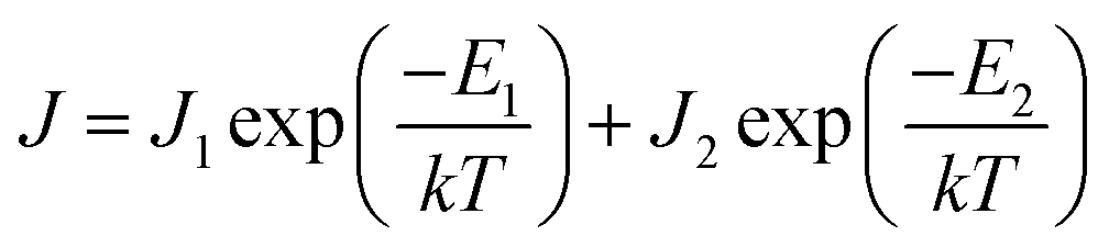 | (3) |
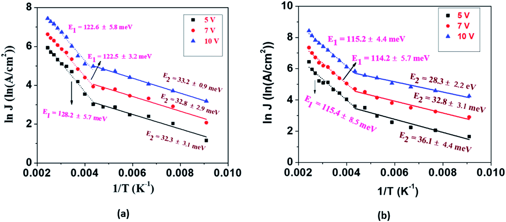 | ||
| Fig. 4 Logarithm of current density (J) as a function of the reciprocal of the temperature between 110 K and 410 K at 3 different bias voltages (a) for individual EGTNT and (b) for individual DMTNT showing intermediate deep and shallow donor levels E1 and E2, respectively. The symbols are the experimental data and the straight lines and dotted lines are the linearly fitted curves to the data. | ||
The values of activation energies derived from the slope of the lnJ vs. 1/T plot at 10 V are E1 ∼ 122 ± 5 meV and E2 ∼ 33 ± 1 meV for EGTNT and E1 ∼ 115 ± 4 meV and E2 ∼ 28 ± 2 meV for DMTNT. It should be mentioned that these values are almost similar for other bias voltages, i.e., 5 V and 7 V. These observations indicate that there exist two trap levels consisting of deep intermediate donors and shallow donors associated with the activation energy of E1 and E2, respectively. At T > 290 K (i.e., 1/T < 0.0034 K−1), both types of donor levels are activated by injecting charges into the conduction band that take part in the electrical conduction. As the temperature decreases below 230 K (i.e., 1/T > 0.0043 K−1), the donors at deep intermediary levels are no longer available even though the shallow donors contribute to the charge transport.
It should be mentioned that the obtained values of E1 and E2 for both EGTNT and DMTNT are in decent agreement with the localized trap state of 133 meV below the CB state and activation energy of 28 meV as reported previously by Mohammadpour et al.45 and Chen et al.,46 respectively. The magnitudes of the activation energy correspond to shallow impurities, for example, oxygen vacancies, which are introduced during the growth or annealing process of the TiO2 nanotubes. A substantial quantity of oxygen vacancies gives rise to a significant distribution of the donor or ionization energy levels, and consequently, the impurity band gets created. Previously, an activation energy of 58 meV for TiO2 nanowires was obtained by Baik et al.,47 and Rothschild et al.48 reported activation energy values of 0.01–0.69 eV with the variation of the ambient air pressure for nanocrystalline TiO2 films. So, it should be pointed out that TiO2 nanostructures grown by diverse methods (synthesized by different processes) and under different conditions can have dissimilar donor concentrations resulting in various values of the activation energy. Despite having a similar crystal structure (XRD patterns showing the anatase phase of both EGTNT and DMTNT are presented in Fig. S1 in the ESI†), the charge flow along the EGTNT encounters inter wall boundaries because of the double-wall morphology, while the charges flowing through the DMTNT see a relatively smoother conduction pathway, leading to lower activation energy values compared to their EGTNT counterparts. Although the morphological difference in EGTNT and DMTNT has been reported in the literature, our data present the first detailed analysis of the temperature-dependent transport and activation energy determination for the observed morphological variation.
In a semiconducting material such as TiO2, donor density Nd plays a direct role in determining the current–voltage characteristics which in turn control the device behavior. The donor density is therefore of primary significance for the determination of electrical properties. A direct experimental determination is challenging due to the involvement of a number of factors. For example, Mott–Schottky measurements provide information about Nd, but the actual interfacial surface area of the semiconductor contact with the electrolyte is very difficult to determine accurately. However, we can approximate the shallow and intermediate donor concentrations from the extracted J2 value (associated with E2) and J1 value (associated with E1) in eqn (3). We can estimate the pre-factors J1 and J2 from the intercept of the lnJ vs. 1/T plot, which can be related with the donor density Nd as
| J = NdqμE | (4) |
| Type of nanotube | Value of E1 (meV) | Value of E2 (meV) | Value of Nd1 (cm−3) | Value of Nd2 (cm−3) |
|---|---|---|---|---|
| EGTNT | 132.1 | 32.9 | 2.56 × 10¹⁸ | 3.65 × 10¹⁶ |
| DMTNT | 115.2 | 28.3 | 4.44 × 10¹⁸ | 5.59 × 10¹⁶ |
The strikingly different morphologies of TiO2 NTs synthesized via anodization depending on the electrolytes used were reported by Liu et al.50 The ‘single-walled’ NT is DMSO based and ‘double-walled’ NT grows in the EG electrolyte. The EG based electrolyte is widely used23 in TNT synthesis and results in double-walled structures with prolonged growth and partial crystallization of the tubes during the growth process. The schematic representation of single-walled and double-walled morphology for DMTNT and EGTNT is displayed in Fig. 5(a) and (b), respectively. SEM images of the bottom part and top part are shown in Fig. 5 showing the variation of the inner diameter from the upper to the lower part of the nanotube arrays to demonstrate the difference in wall morphology.
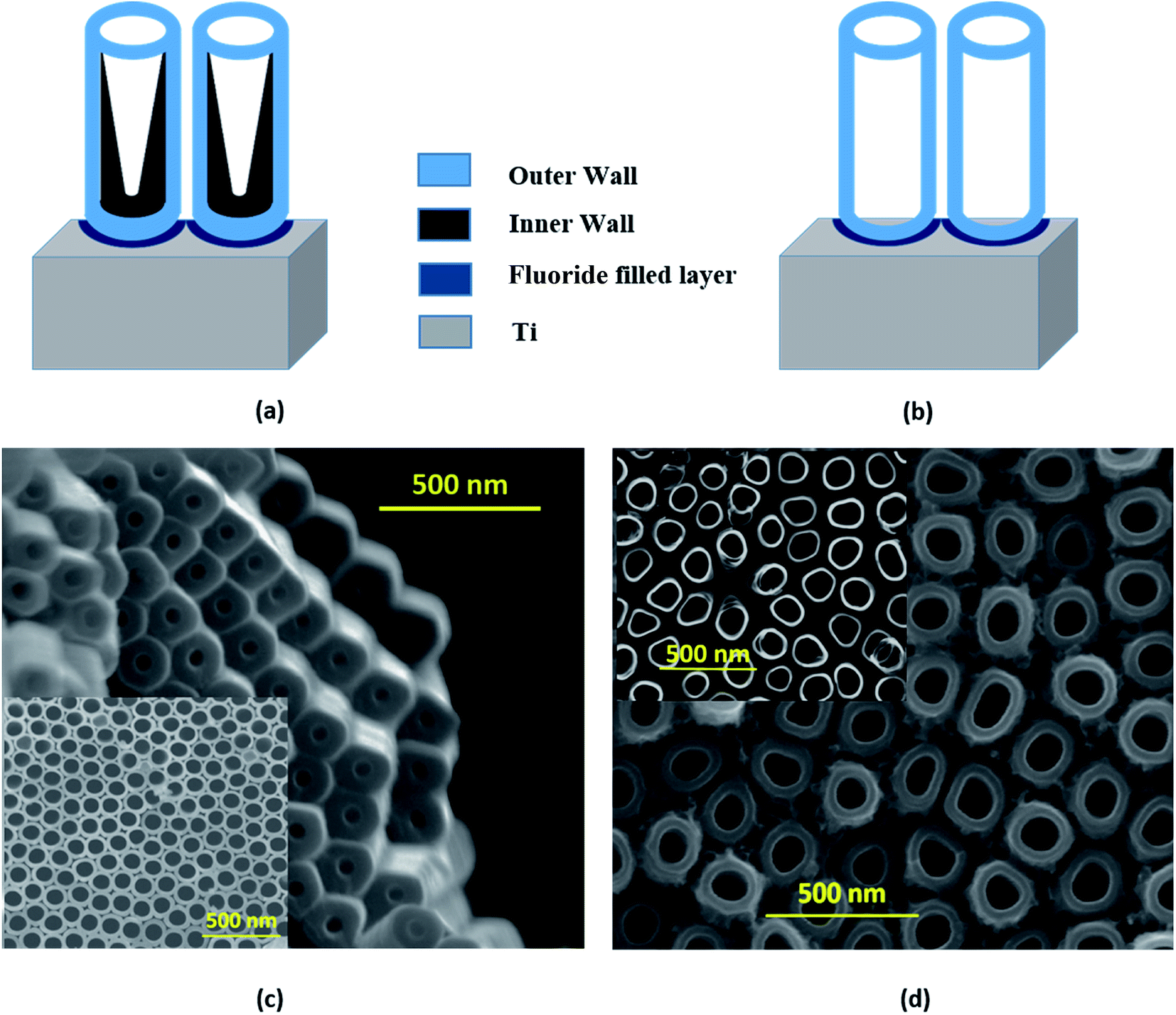 | ||
| Fig. 5 Schematic representation of the double walled and single walled morphology for (a) EGTNT and (b) DMTNT, respectively. SEM images of the bottom part and top part (inset) of (c) EGTNT and (d) DMTNT showing the variation of the pore diameter from the top part to the bottom part for the nanotube arrays. | ||
During anodization at a voltage of 60 V, substances decomposed from EG and fluoride ions feasibly undergo reaction with Ti4+ ions at the EG–TiO2 boundary and develop the interior wall50 of the DWNT, consequently increasing the carbon impurities. The double-walled feature of the tubes becomes noticeable in the SEM images after annealing. To avoid the development of the contaminated inner wall, we should use the type of electrolyte (i.e., DMSO mixed with HF) that leads to a greater extent of Ti4+ dissolution and also limits the formation of undissolved residues. As suggested by Mirabolghasemi et al.,51 a DMSO based electrolyte has the capability to dissolve by-products formed during anodization.
When the nanotubes are formed in DMSO electrolytes, they have a larger inner diameter with persistent wall thickness all the way through the whole length (Fig. 5(c)). The residual debris like carbon or fluorine species gets trapped in the inner shell and gets dissolved in the form of [TiF6]2−. The inner wall becomes thinner towards the tube top, indicating complete decomposition of the debris near the tube opening. Post the annealing process, the single-walled tubes show considerably different physical properties than their double-walled counterparts. It was reported by Mirabolghasemi et al.51 that the annealed SWNT reveal a substantial enhancement of their electrical conductivity compared to DWNT, which has also been reflected in our experiments, where the conductivity of individual SWNT is much higher than its DWNT counterpart. The variation of activation energies (E1 and E2, as shown in Table 2) in EGTNT and DMTNT can be understood by considering this morphological variation of the walls of the nanotubes.
Catastrophic breakdown in the TiO2 nanotube
During the I–V measurements on single nanotubes, we observed physical breakdown (breaking or collapse) under certain conditions, which are presented in Fig. 6–8. In order to understand the capability and limitations of charge transport through these nanostructures, we need to analyze such breakdowns in greater detail.Tian et al. recently reported HR-TEM studies of the breakdown in TiO2 nanocrystals.52In situ microscopy was performed to understand the physical characteristics associated with such breakdowns in TiO2 nanocrystals. In the case of TiO2 nanotubes, however, we have observed three types of J–V plots during the breakdown, which are described as ‘Model A’ (Fig. 6), ‘Model B’ (Fig. 7) representing single DMTNT, and ‘Model C’ (Fig. 8) representing a bundle of EGTNT. In general (common to all figures), at lower applied potential (less than 1 V), the current density J is almost linear and subsequently becomes nonlinear with an increase in voltage which finally culminates in breakdown through three different approaches.
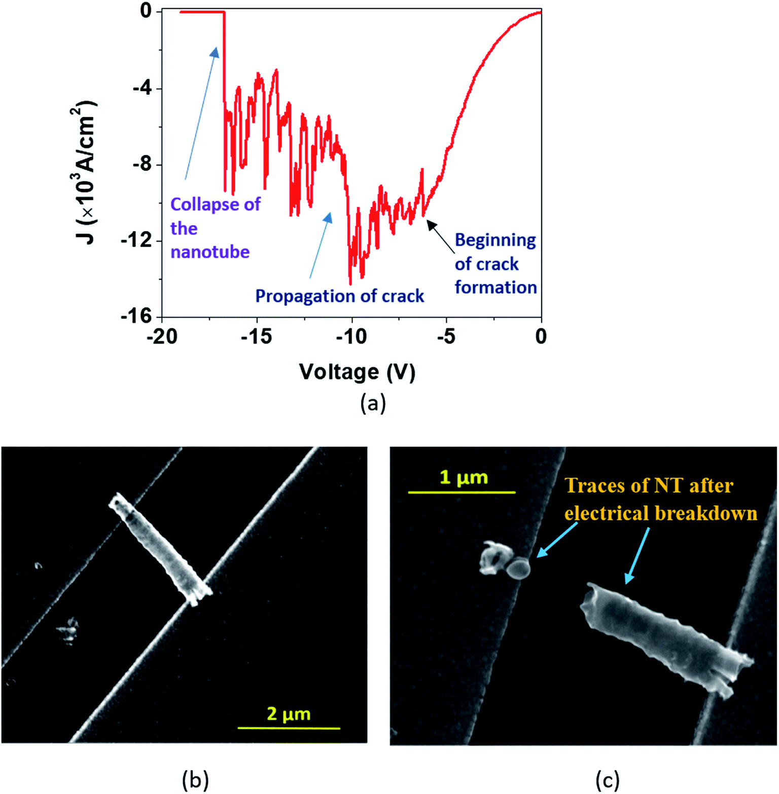 | ||
| Fig. 6 (a) In the ‘Model A’ breakdown, the J–V curve displays features of an exponential rise in J along with nonlinearity before the verge of breakdown and reveals a stepwise fall of J during the electrical breakdown. SEM images exhibit a single DMTNT (b) before and (c) after the breakdown. | ||
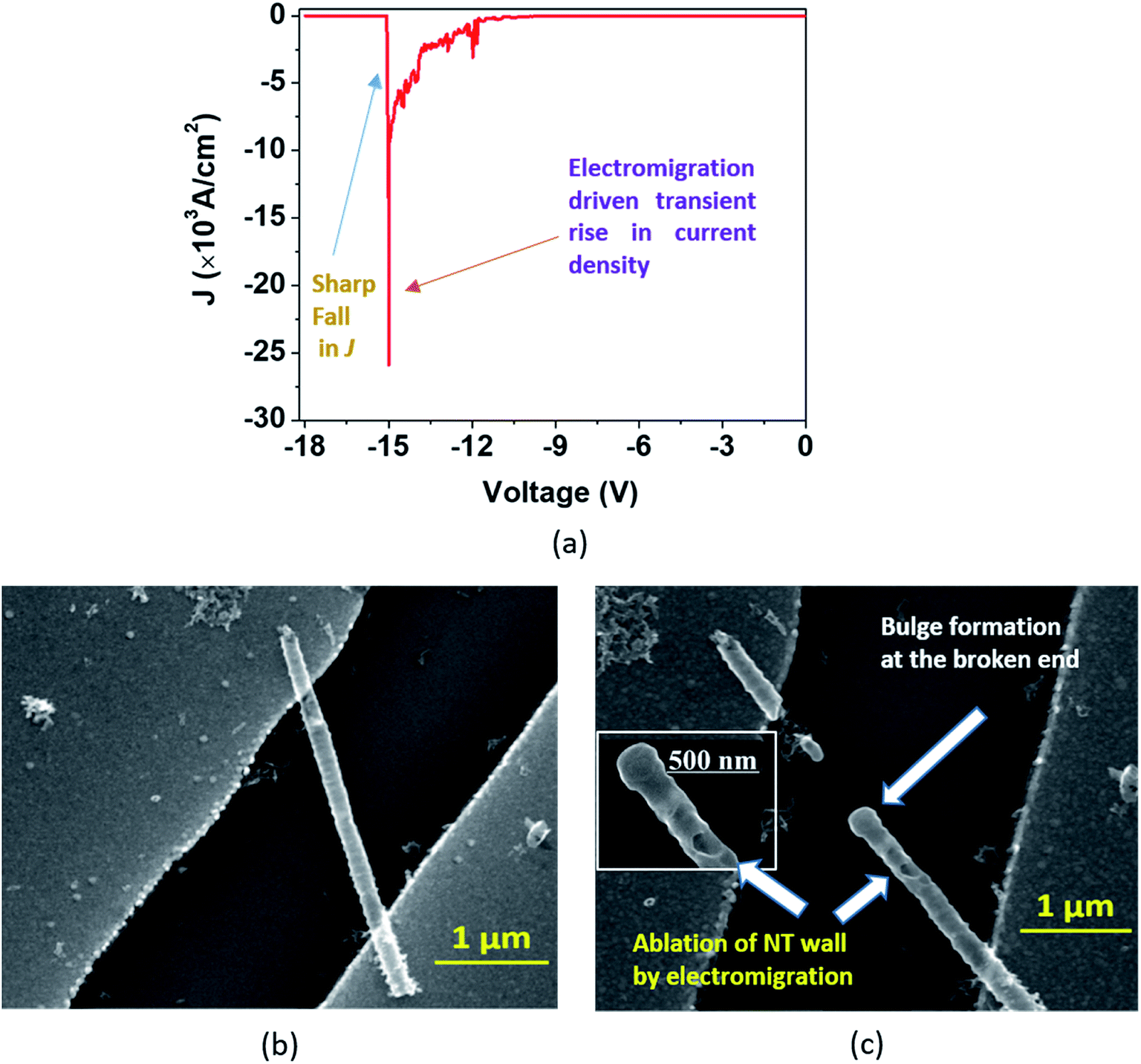 | ||
| Fig. 7 (a) In the ‘Model B’ breakdown, the J–V curve displays a sharp transient rise in J before the breakdown point and a sharp fall after the breakdown. SEM images show a single DMTNT (b) before and (c) after the breakdown. Bulge formation occurs at the broken end of the NT due to excessive heat dissipation as shown in (c); magnified image of the broken end in the inset of (c). | ||
 | ||
| Fig. 8 (a) In ‘Model B’ type breakdown, gradual variation in voltage (0 → 10 V → 0 V) before the onset of breakdown. The bias direction 0 → 5 V → 0 V is shown in the inset. (b) The transient rise in J is evidence of the onset of electromigration through a single TiO2 nanotube; the I–V characteristics corresponding to the J–V curve are shown in the inset. The FESEM images showing an individual TiO2 nanotube (c) before and (d) after the breakdown; the breakdown point of the NT becomes distorted resulting in bulge formation as shown in (d). | ||
In the first approach (Model ‘A’, Fig. 6), a small transient increase of J up to −6.2 V followed by a stepwise rise up to the breakdown point (−10 V) and then a fall to zero with a non-uniform step by step decrease (−10 V to −16.6 V) is observed. The SEM images of a single NT before and after the breakdown are shown in Fig. 6(b) and (c). The stepwise reduction of J may signify crack formation and its progress in the wall of TiO2 NTs, leading to collapse, which we label ‘Model A’ breakdown. The noisy nature of the current density profile is directly related to the creation of “breakdown paths” or cracks, which possibly induce trapping and de-trapping of charge carriers. The charges, unable to obtain an easy pathway, start accumulating, leading to a local ‘hot zone’ that creates further cracks. The movement of charges is now governed by the creation of these cracks that are reflected in the fluctuations in the J–V characteristics. It is apparent that the crack formation is dominant at the end of the nanotubes near the electrodes. This is caused by the charge injection from the contact leading to a higher probability of accumulation around this region. Such accumulation and the local heating effect at the nanotube/electrode interface53 have been reported. Also, the thermal conductivity of the TiO2 NT and Au film is 1.12 W m−1 K−1 (ref. 54) and 160 W m−1 K−1,55 respectively. This results in a high thermal conductance difference at the TNT–Au electrode interface (small contact area), resulting in a temperature gradient. Therefore, only the region near the end of the nanotube close to the contact reaches a very high temperature close to the melting point.
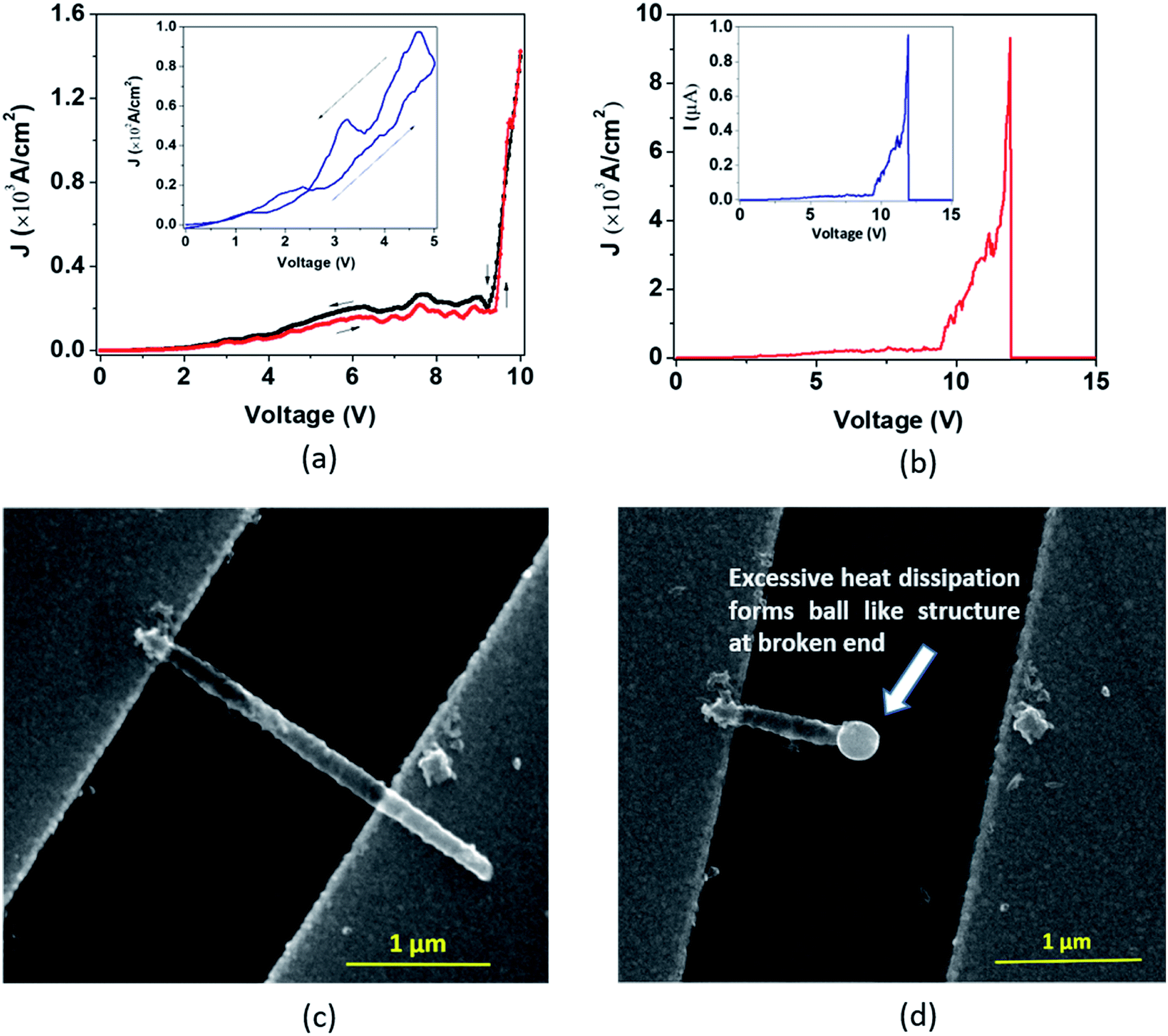
In the second type of breakdown marked ‘Model B’, the current density J shows a transient rise up to a maximum value (Jbreak), followed by a sharp fall to zero (Fig. 7(a)). The morphologies of the nanotube before and after breakdown are shown in Fig. 7(b) and 7(c), respectively. A careful observation reveals that at the point of breakdown shown in Fig. 7(c), a spherical bulge is formed that indicates outward pressure on the walls of the nanotubes. We now attempt to analyze the sharp increase in the current density and consequent collapse that has not been reported so far for individual TiO2 NTs. The J–V measurement (Fig. 8(a)) in the pre-breakdown region was performed by slowly increasing the bias up to the maximum point (near the breakdown voltage) and reducing it back to zero. As seen in the inset of Fig. 8(a), the J–V curve is almost entirely reversible up to a bias of 1.28 V, but the noisy nature of J after this (5 to 9 V, Fig. 8(a)) may indicate reformation of the NT/Au junction region. As we increase the bias further, an abrupt increase in J occurs (9 to 10 V). However, when we decrease the bias (10 to 0 V), the J–V curve almost follows the earlier pattern (0 to 10 V) but with a small upward shift (Fig. 8(a)) indicating the flow of charges along a new and less resistive path.
A further increase in the bias results in a sharp rise in J (11.3 V to 11.9 V, Fig. 8(b)) to the breakdown value (Jbreak, the value of current density at which breakdown occurs, is 9.32 × 10³ A cm−2) and then it falls abruptly to zero. Such a transient increase in the current density observed in our experiments gives evidence of the occurrence of explicit, permanent changes in the nanotube at the onset of the breakdown.
A current transient observed in the ‘Model B’ type breakdown is attributed to a reformation of the NT–metal electrode contact. Electromigration56–58 (the movement of atoms/ions under the influence of an electric field) of metal atoms under high bias is a probable cause for this type of collapse. Electric field and localized heating driven electromigration of thermally diffused metal ions from the contact and Ti ions in the nanotube leads to collapse (breakdown) at the most defective region of the wall as seen in the ‘Model B’ (Fig. 7(c)) breakdown. A breakdown field of 104 V cm−1 (Fig. 7(a)) is large enough to cause electromigration in metals such as Ag, Cu, Au, In, Pb, and Mg.59 Such behavior resembles the previously reported phenomenon observed in CNTs by Chiu et al.60 As the metal ions migrate through the nanotube under high bias, they create defects and generate more heat, as a result of which the NT wall collapses with formation of a bulge as observed in Fig. 7(c) and 8(d). The asymmetric thermal gradient also plays a role in defining the breakdown region (hottest spot) and melting the NTs at the hottest spot.61
In the case of a bundle of nanotubes, however, we observed a mixed feature of stepwise increase followed by a transient rise in J up to a maximum value. The decrease of current density also follows a mixed pattern of stepwise and sharp falls; such behavior is termed ‘Model C’ type breakdown (Fig. 9(a)). The FESEM images show a bundle of EGTNT before (Fig. 9(b)) and after breakdown (Fig. 9(c)). Table 3 presents typical values of breakdown voltage and current for each type of breakdown.
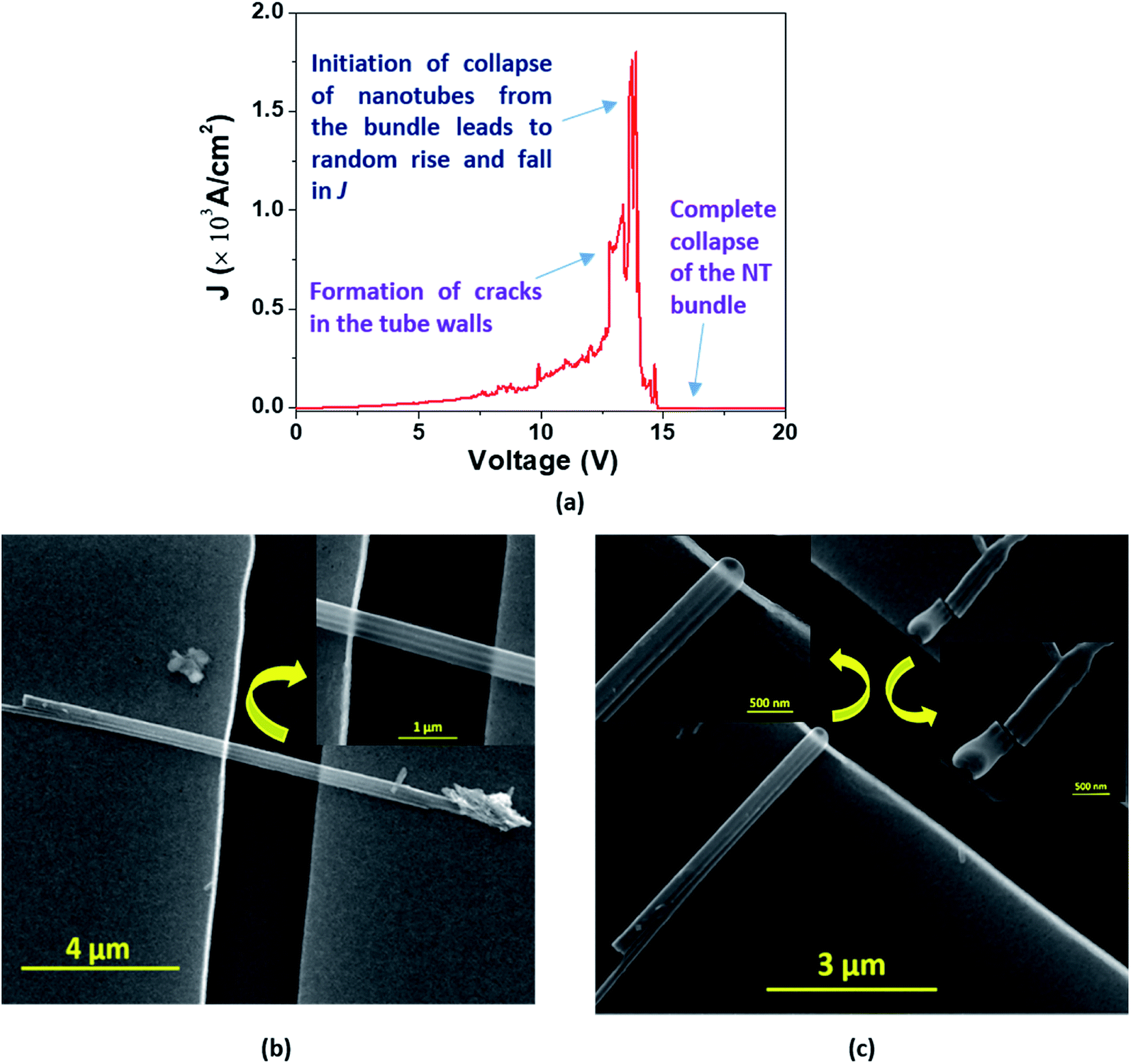 | ||
| Fig. 9 (a) In the ‘Model C’ breakdown, the J–V curve displays mixed features of nonlinearity along with sudden big steps in J before the breakdown point which may be the characteristics for breaking of the bridge between the nanotubes in the bundle. SEM images exhibit a bundle of 3 EGTNT (b) before and (c) after the breakdown; magnified SEM images are also displayed in the insets. | ||
| Type of NT breakdown | V break (V), Ibreak (A) | Breakdown power Pbreak (μW) |
|---|---|---|
| ‘Model A’ | 10, 1.40 × 10⁻⁶ | 14.6 |
| ‘Model B’ | 15, 2.61 × 10⁻⁶ | 39.8 |
| ‘Model C’ | 13, 0.50 × 10⁻⁶ | 6.9 |
The chance of electrical failure becomes enhanced if there are more defects or contaminants within the NTs,62 and the defect free tubes are mostly good conductors of heat. This agrees with our measurements for TNTs as we have seen that the complete or partial ablation of the NT wall occurred primarily on DMTNT during J–V measurements as it has a rough wall morphology, which most probably increases the surface defects. The breakdown power in the μW range is sufficient to break these metal oxide nanotubes, which means they cannot sustain high power compared to extremely conducting carbon nanotubes63 (mW range).
As the nanotubes are suspended on two metal contact pads, the absence of a substrate beneath them constrains heat dissipation only through the surface of the NTs, the electrodes, and the neighboring environment.64 As J–V measurements have been performed in a vacuum atmosphere, the heat dissipation happens mostly through the NT and the electrodes. Also, it has been observed that the extremely resistive part of the NT is broken at a lower current which indicates that breakdown does not always occur at the middle part,65 and also for shorter NTs, this happens away from the central part of the NT66 due to the anisotropic temperature profile.
The breakdown current density Jbreak (Table 3) for a single nanotube of different morphologies may be explained using the one-dimensional thermal transport model64,65 which is expressed as
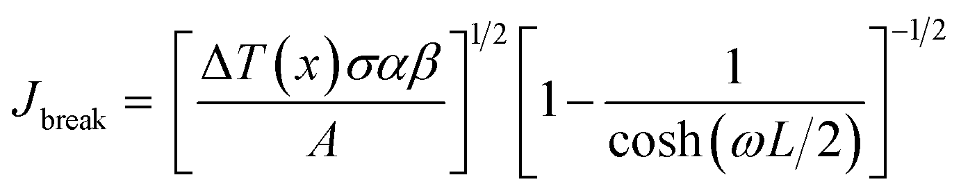 | (5) |
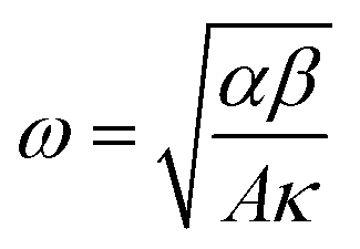 , κ is the thermal conductivity of the NT, and L is the length of the NT. For our suspended NT configuration,
 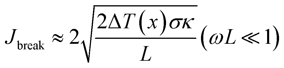 ,67 which shows that Jbreak is proportional to the square root of the electrical conductivity (σ) and thermal conductivity of the nanotube. This explains that a lower Jbreak is sufficient to break highly resistive NTs, and this is reflected in our results (Table 3) where a comparatively less conducting bundle of EGTNT breaks down at a lower Jbreak compared to individual DMTNT, supporting the one-dimensional thermal transport model.
Conclusions
In conclusion, TiO2 nanotubes with two distinct morphologies, smooth and rough, having single and double-walled characteristics, have been successfully fabricated into individual nanotube devices. The contacts are prepared by photolithography without using complex processes such as electron beam lithography or focused ion beam deposition. The electrical conduction process at the lower temperature regime (110 < T < 230 K) and higher temperature regions (T > 230 K) depends on two thermal activation processes attributed to shallow and intermediate deep donors, respectively, and the average values of the activation energies are E1 ∼ 122 ± 5 meV and E2 ∼ 33 ± 1 meV for EGTNT and E1 ∼ 115 ± 4 meV and E2 ∼ 28 ± 2 meV for DMTNT. Furthermore, the physical breakdown of the nanotubes observed at higher bias has been analyzed. The J–V measurements reveal three distinct types of electrical breakdown associated with the physical collapse of the TiO2 NTs. In ‘Model A’ type breakdown, a stepwise rise in current density J up to the breakdown point followed by a non-uniform stepwise decrease is observed which is caused by crack formation in the NT wall. In ‘Model B’ type breakdown, electric field and localized heating driven electromigration of thermally diffused metal ions from the contact and Ti ions in the nanotube leads to collapse (breakdown) at the most defective region of the wall. Finally, in ‘Model C’ type breakdown observed in a bundle of nanotubes, the J–V characteristics show mixed features of the ‘Model A’ and ‘Model B’ type breakdown. This study offers insight into the morphology dependent electrical transport in single TiO2 nanotubes and also opens up the possibility of devices based on TiO2 nanotubes. Further, the breakdown mechanisms investigated in this work help to define compliance and limitations of such nanotube devices.Conflicts of interest
There are no conflicts to declare.Acknowledgements
The authors acknowledge the Center for NEMS and Nanophotonics, IIT Madras for providing resources for fabrication and characterization and the scanning electron microscope facility (FE-SEM) partly sponsored by the DST-FIST program. SK is thankful to Deepak Bhat and Sanjoy Jena for their initial help in the fabrication and Dr Soumya Dutta and Mithun, C. A. for measurements at the cryo-probe station.References
- Y. Li, F. Qian, J. Xiang and C. M. Lieber, Mater. Today, 2006, 9, 18–27 CrossRef CAS.
- G. K. Mor, K. Shankar, M. Paulose, O. K. Varghese and C. A. Grimes, Nano Lett., 2006, 6, 215–218 CrossRef CAS.
- H. S. Kim, J. W. Lee, N. Yantara, P. P. Boix, S. A. Kulkarni, S. Mhaisalkar, M. Grätzel and N. G. Park, Nano Lett., 2013, 13, 2412–2417 CrossRef CAS.
- X. Duan, Y. Huang, R. Agarwal and C. M. Lieber, Nature, 2003, 421, 241–245 CrossRef CAS.
- W. Li, C. Liang, W. Zhou, J. Qiu, Z. Zhou, G. Sun and Q. Xin, J. Phys. Chem. B, 2003, 107, 6292–6299 CrossRef CAS.
- M. C. Mcalpine, H. Ahmad, D. Wang and J. R. Heath, Nat. Mater., 2007, 6, 379–384 CrossRef CAS.
- J. Chen, L. Xu, W. Li and X. Gou, Adv. Mater., 2005, 17, 582–586 CrossRef CAS.
- Q. Kuang, C. Lao, L. W. Zhong, Z. Xie and L. Zheng, J. Am. Chem. Soc., 2007, 129, 6070–6071 CrossRef CAS.
- M. D. Kelzenberg, D. B. Turner-Evans, B. M. Kayes, M. A. Filier, M. C. Putnam, N. S. Lewis and H. A. Atwater, Nano Lett., 2008, 8, 710–714 CrossRef CAS.
- J. Bao, M. A. Zimmler, F. Capasso, X. Wang and Z. F. Ren, Nano Lett., 2006, 6, 1719–1722 CrossRef CAS.
- S. J. Tans, A. R. M. Verschueren and C. Dekker, Nature, 1998, 393, 49–52 CrossRef CAS.
- A. L. Linsebigler, G. Lu and J. T. Yates, Chem. Rev., 1995, 95, 735–758 CrossRef CAS.
- D. Deng, M. G. Kim, J. Y. Lee and J. Cho, Energy Environ. Sci., 2009, 2, 818–837 RSC.
- M. H. Seo, M. Yuasa, T. Kida, J. S. Huh, K. Shimanoe and N. Yamazoe, Sens. Actuators, B, 2009, 137, 513–520 CrossRef CAS.
- S. Rani, S. C. Roy, M. C. Bhatnagar and D. Kanjilal, in Proceedings of IEEE Sensors, 2008 Search PubMed.
- S. U. M. Khan, M. Al-Shahry and W. B. Ingler, Science, 2002, 297, 2243–2245 CrossRef CAS.
- G. K. Mor, K. Shankar, M. Paulose, O. K. Varghese and C. A. Grimes, Nano Lett., 2005, 5, 191–195 CrossRef CAS.
- A. Fujishima and K. Honda, Nature, 1972, 238, 37–38 CrossRef CAS.
- P. Chen, J. Brillet, H. Bala, P. Wang, S. M. Zakeeruddin and M. Grätzel, J. Mater. Chem., 2009, 19, 5325–5328 RSC.
- B. Oregan and M. Gratzel, Nature, 1991, 353, 737–740 CrossRef CAS.
- O. K. Varghese, M. Paulose and C. A. Grimes, Nat. Nanotechnol., 2009, 4, 592–597 CrossRef CAS.
- S. Farsinezhad, A. Mohammadpour, A. N. Dalrymple, J. Geisinger, P. Kar, M. J. Brett and K. Shankar, J. Nanosci. Nanotechnol., 2013, 13, 2885–2891 CrossRef CAS.
- S. Rani, S. C. Roy, M. Paulose, O. K. Varghese, G. K. Mor, S. Kim, S. Yoriya, T. J. Latempa and C. A. Grimes, Phys. Chem. Chem. Phys., 2010, 12, 2780–2800 RSC.
- K. Lee, A. Mazare and P. Schmuki, Chem. Rev., 2014, 114, 9385–9454 CrossRef CAS.
- H. Tsuchiya and P. Schmuki, Nanoscale, 2020, 12, 8119–8132 RSC.
- C. Fàbrega, F. Hernández-Ramírez, J. Daniel Prades, R. Jiménez-Díaz, T. Andreu and J. Ramon Morante, Nanotechnology, 2010, 21, 445703 CrossRef.
- M. Stiller, J. Barzola-Quiquia, I. Lorite, P. Esquinazi, R. Kirchgeorg, S. P. Albu and P. Schmuki, Appl. Phys. Lett., 2013, 103, 1–5 CrossRef.
- M. Hattori, K. Noda, T. Nishi, K. Kobayashi, H. Yamada and K. Matsushige, Appl. Phys. Lett., 2013, 102, 1–5 Search PubMed.
- M. Lee, D. Cha, J. Huang, M.-W. Ha and J. Kim, Jpn. J. Appl. Phys., 2016, 55, 06GG11 CrossRef.
- H. Brahmi, R. Neupane, L. Xie, S. Singh, M. Yarali, G. Katwal, S. Chen, M. Paulose, O. K. Varghese and A. Mavrokefalos, Nanoscale, 2018, 10, 3863–3870 RSC.
- S. Yoriya, M. Paulose, O. K. Varghese, G. K. Mor and C. A. Grimes, J. Phys. Chem. C, 2007, 111, 13770–13776 CrossRef CAS.
- S. P. Albu and P. Schmuki, Phys. Status Solidi RRL, 2010, 4, 215–217 CrossRef CAS.
- D. Cha, M. Lee, H. Shin, M. J. Kim and J. Kim, Microsc. Microanal., 2009, 15, 1180–1181 CrossRef.
- M. Enachi, O. Lupan, T. Braniste, A. Sarua, L. Chow, Y. K. Mishra, D. Gedamu, R. Adelung and I. Tiginyanu, Phys. Status Solidi RRL, 2015, 9, 171–174 CrossRef CAS.
- D. Wisniewski, K. Byrne, C. F. De Souza, C. Fernandes and H. E. Ruda, Nanotechnology, 2019, 30, 054007 CrossRef CAS.
- C. Opoku, A. S. Dahiya, G. Poulin-Vittrant, N. Camara and D. Alquier, Phys. Status Solidi A, 2016, 213, 2438–2445 CrossRef CAS.
- P. P. Vijayan, M. Thomas and K. C. George, J. Appl. Phys., 2012, 112, 104308 CrossRef.
- C. Jia, F. Yang, L. Zhao, G. Cheng and G. Yang, Nanoscale Res. Lett., 2019, 14, 10 CrossRef.
- L. Hu, L. Wu, M. Liao, X. Hu and X. Fang, Adv. Funct. Mater., 2012, 22, 998–1004 CrossRef CAS.
- L. Q. Mai, C. S. Lao, B. Hu, J. Zhou, Y. Y. Qi, W. Chen, E. D. Gu and Z. L. Wang, J. Phys. Chem. B, 2006, 110, 18138–18141 CrossRef CAS.
- J. R. Yeargan and H. L. Taylor, J. Appl. Phys., 1968, 39, 5600–5604 CrossRef CAS.
- W. Yang, J. Marino, A. Monson and C. A. Wolden, Semicond. Sci. Technol., 2006, 21, 1573–1579 CrossRef CAS.
- I. Ali, M. Suhail, Z. A. Alothman and A. Alwarthan, RSC Adv., 2018, 8, 30125–30147 RSC.
- J. Kuchařik, H. Sopha, M. Krbal, I. Rychetský, P. Kužel, J. M. Macak and H. Němec, J. Phys. D: Appl. Phys., 2018, 51, 014004 CrossRef.
- R. Mohammadpour, J. Phys. D: Appl. Phys., 2017, 50, 505106 CrossRef.
- R. S. Chen, C. A. Chen, W. C. Wang, H. Y. Tsai and Y. S. Huang, Appl. Phys. Lett., 2011, 99, 2011–2014 Search PubMed.
- J. M. Baik, M. H. Kim, C. Larson, X. Chen, S. Guo, A. M. Wodtke and M. Moskovits, Appl. Phys. Lett., 2008, 92, 90–93 CrossRef.
- A. Rothschild, Y. Komem, A. Levakov, N. Ashkenasy and Y. Shapira, Appl. Phys. Lett., 2003, 82, 574–576 CrossRef CAS.
- R. S. Chen, C. A. Chen, W. C. Wang, H. Y. Tsai and Y. S. Huang, Appl. Phys. Lett., 2011, 99, 222107 CrossRef.
- N. Liu, H. Mirabolghasemi, K. Lee, S. P. Albu, A. Tighineanu, M. Altomare and P. Schmuki, Faraday Discuss., 2013, 164, 107–116 RSC.
- H. Mirabolghasemi, N. Liu, K. Lee and P. Schmuki, Chem. Commun., 2013, 49, 2067–2069 RSC.
- X. Tian, G. L. Brennecka and X. Tan, ACS Nano, 2020, 14, 8328–8334 CrossRef CAS.
- M. M. Yazdanpanah, S. Chakraborty, S. A. Harfenist, R. W. Cohn and B. W. Alpnenaar, Appl. Phys. Lett., 2004, 85, 3564–3566 CrossRef CAS.
- L. Guo, J. Wang, Z. Lin, S. Gacek and X. Wang, J. Appl. Phys., 2009, 106, 123526 CrossRef.
- Q. G. Zhang, B. Y. Cao, X. Zhang, M. Fujii and K. Takahashi, Phys. Rev. B: Condens. Matter Mater. Phys., 2006, 74, 1–5 Search PubMed.
- W. Y. Jang, N. N. Kulkarni, C. K. Shih and Z. Yao, Appl. Phys. Lett., 2004, 84, 1177–1179 CrossRef CAS.
- A. Fujii, M. Tsutsui, S. Kurokawa and A. Sakai, Phys. Rev. B: Condens. Matter Mater. Phys., 2005, 72, 1–6 Search PubMed.
- H. Park, A. K. L. Lim, A. P. Alivisatos, J. Park and P. L. McEuen, Appl. Phys. Lett., 1999, 75, 301–303 CrossRef CAS.
- H. M. Breitling, J. Phys. Chem. Solids, 1972, 33, 845–852 CrossRef CAS.
- H. Y. Chiu, V. V. Deshpande, H. W. C. Postma, C. N. Lau, C. Mikó, L. Forró and M. Bockrath, Phys. Rev. Lett., 2005, 95, 1–4 CrossRef.
- C. Kim, D. Kang, T. Y. Lee, K. H. P. Kim, Y. S. Kang, J. Lee, S. W. Nam, K. B. Kim and Y. Khang, Appl. Phys. Lett., 2009, 94, 92–95 Search PubMed.
- P. Poncharal, C. Berger, Y. Yi, Z. L. Wang and W. A. De Heer, J. Phys. Chem. B, 2002, 106, 12104–12118 CrossRef CAS.
- M. Tsutsui, Y. K. Taninouchi, S. Kurokawa and A. Sakai, J. Appl. Phys., 2006, 100, 094302 CrossRef.
- M. A. Kuroda, A. Cangellaris and J. P. Leburton, Phys. Rev. Lett., 2005, 95, 1–4 CrossRef.
- G. K. Goswami and K. K. Nanda, AIP Adv., 2012, 2, 022129 CrossRef.
- A. Liao, R. Alizadegan, Z. Y. Ong, S. Dutta, F. Xiong, K. J. Hsia and E. Pop, Phys. Rev. B: Condens. Matter Mater. Phys., 2010, 82, 1–9 Search PubMed.
- H. Kitsuki, T. Yamada, D. Fabris, J. R. Jameson, P. Wilhite, M. Suzuki and C. Y. Yang, Appl. Phys. Lett., 2008, 92, 2006–2009 CrossRef.
Footnote |
| † Electronic supplementary information (ESI) available. See DOI: 10.1039/d0na00713g |
| This journal is © The Royal Society of Chemistry 2021 |