DOI:
10.1039/D0NA00682C
(Paper)
Nanoscale Adv., 2020,
2, 5848-5856
Observing quantum trapping on MoS2 through the lifetimes of resonant electrons: revealing the Pauli exclusion principle†
Received
19th August 2020
, Accepted 11th November 2020
First published on 11th November 2020
Abstract
We demonstrate that the linewidth of the field emission resonance (FER) observed on the surface of MoS2 using scanning tunneling microscopy can vary by up to one order of magnitude with an increasing electric field. This phenomenon originates from quantum trapping, in which the electron relaxed from a resonant electron in the FER is momentarily trapped in a potential well on the MoS2 surface due to its wave nature. Because the relaxed electron and the resonant electron have the same spin, through the action of the Pauli exclusion principle, the lifetimes of the resonant electrons can be substantially prolonged when the relaxed electrons engage in resonance trapping. The linewidth of the FER is thus considerably reduced to as narrow as 12 meV. The coexistence of the resonant electron and the relaxed electron requires the emission of two electrons, which can occur through the exchange interaction.
1. Introduction
In quantum mechanics, two cases are considered in the model of a square potential well. One case is quantum confinement, in which the particle energy is lower than the well depth. The wave function of a particle in the well is a standing wave, and its energy states are quantized. The other case is quantum scattering, in which a free particle is scattered by the well. Because of the wave nature, only particles with specific energies can pass through the well without reflection; this is called resonance transmission. In reality, quantum confinement and quantum scattering can be observed in metallic films whose electronic structures have free-electron properties.1–10 Herein, we report a new case called quantum trapping, in which a particle is in the well but has energy higher than the well depth. In this case, the particle can be temporarily trapped in the well; however, it can eventually escape from the well because of wave function dissipation. The mean duration for which the well traps the particle varies with the well size in oscillation. We demonstrate that quantum trapping can be experimentally revealed through the linewidth of the field emission resonance (FER)11,12 observed on the surface of bulk MoS2 by using scanning tunneling microscopy (STM).
FER is a phenomenon in which electrons emitted from an STM tip due to a strong electric field enter the quantized standing wave state in the STM junction, becoming resonant electrons. Although the FER originates from the quantized states in a vacuum,13 it can contain information associated with the physical properties of the surface and the STM tip. For example, FER energies can reveal the local work function of the surface.14–20 FER intensities can reflect the local electron transmissivity of the reconstructed surface.21 The zero valley intensities appearing around the FER may indicate that the observed material has a band gap above the vacuum level.21 The number of FERs can manifest the sharpness22–24 and field enhancement factor25 of the STM tip. Previous studies have demonstrated that FER can be used to investigate the atomic structure of an insulator,26 plasmon-assisted electron tunneling,27 and the dynamics28,29 and lateral quantization30–32 of surface electrons above the vacuum level. In this study, we focus on the linewidth of the FER, which has seldom been investigated. The reciprocal of the linewidth can be interpreted as the mean lifetime of resonant electrons staying in the FER state, referring to a similar interpretation for quantum well states in metallic films.3,4
We discovered that the linewidth can modulate with the electric field of the forming FER and suggest that the oscillatory duration in quantum trapping is manifested by this linewidth modulation. The relationship between them is established by the following mechanisms. (1) The lifetime of a resonant electron only terminates with the occurrence of electron relaxation via light emission22,33 because the bulk MoS2 has a band gap above the vacuum level. (2) Per unit time, two resonant electrons with opposite spins are successively emitted from the STM tip through the exchange interaction, and one resonant electron relaxes first. (3) Because of the inhomogeneous electric field resulting from the curvature of the STM tip, the electron relaxed from a resonant electron (named the relaxed electron) has lateral kinetic energy,28 and a local potential well forms beneath the tip on the MoS2 surface. Due to quantum trapping, the potential well temporarily traps the relaxed electron. When the potential well dimension matches the de Broglie wave length of the relaxed electrons, the mean trapping time that the potential well traps the relaxed electrons increases dramatically, manifesting resonance trapping. (4) Both the relaxed electron and the resonant electron have the same spin. According to the Pauli exclusion principle, the resonant electron cannot emit light while the relaxed electron remains trapped in the well, leading to the lifetime of this resonant electron being longer than that of the first one. Accordingly, the variation of the FER linewidth is mainly determined by the mean lifetime of resonant electrons relaxing subsequently.
2. Methods
2.1 STM measurements
A synthesized bulk Nb-doped MoS2 sample (2D semiconductor) was cleaved in air using adhesive tape and then transferred into an ultrahigh vacuum STM operated at 78 K (bulk MoS2 is an insulator at 5 K). FERs were observed by using a PtIr tip to perform Z–V spectroscopy under a current of 10 pA. Differentiation of the Z–V spectrum was executed using a numerical method to reveal FERs. It was not necessarily to immediately observe FERs when Z–V spectroscopy was performed. Whenever FERs did not appear, the method of applying a voltage pulse was used to improve the tip condition. Once FERs appeared on a clean area, we repeatedly took the spectra at different locations. Usually we could obtain hundreds of spectra before the FERs disappeared again. By inspecting the aspects of these spectra, we found that similar spectra could appear a few times. Then, the spectrum would spontaneously change into a different spectrum with FERs of disparate energies and shapes. Based on the similarity, hundreds of spectra could be divided into tens of groups. Similar spectra in each group were superposed to form one spectrum for analysis. The change of FER spectra originated from the spontaneous adjustment of the tip sharpness due to the high electric field at the tip apex and the thermal effect. Because the average period of the sharpness change was much longer than the acquisition time of taking one spectrum, we could obtain similar spectra with clear FERs before the sharpness changed and different spectra under different sharpness levels (see ESI note 1, Fig. S1†). By combining the spontaneous sharpness changes with the voltage pulses, spectra with FERs of different numbers were acquired.
2.2 DFT calculations
The electronic structures were calculated using the projector augmented wave (PAW) approach as implemented in the Vienna Ab initio Simulation Package (VASP) based on density functional theory (DFT). The Perdew–Burke–Ernzerhof (PBE) form of the generalized gradient approximation (GGA) was used for the exchange–correlation functional. The spin–orbit coupling was taken into account in the self-consistent field (SCF) calculations. For the bulk MoS2 calculations, we used a 24 × 24 × 6 Monkhorst–Pack mesh for k-point sampling within the 3D Brillouin zone. A 24 × 24 × 1 Monkhorst–Pack k-mesh over the 2D Brillouin zone was adopted for the 3-layer MoS2 slab calculations with a vacuum thickness of 15 Å well separating the slabs. The cutoff energy for the plane wave basis was set as 280 eV. The energy convergence threshold was set as 10−4 eV in the SCF calculations, while the energy convergence threshold was set as 10−3 eV for the structure optimizations. The electric field-induced valence electron density redistribution was studied by applying a uniform external electric field ranging from 0.0 to 0.3 V Å−1 along the normal to the plane of the MoS2 slab. The out-of-plane charge profile was then obtained by summing the charge density over all grid points for each slice along the plane normal of the MoS2 slab.
3. Results and discussion
3.1 The linewidth of the FER on MoS2
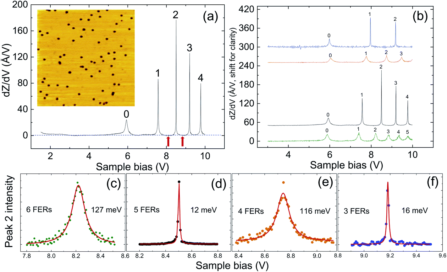
Fig. 1(a) shows a differential Z–V spectrum with five FER peaks observed on a MoS2 surface whose topographic image is displayed in the inset. The numbers represent the orders of the FER peaks. A previous study noted that the potential of the zeroth-order peak is the superposition of the image potential and the external potential, whereas that of higher-order peaks is simply the external potential.14 Thus, the higher-order numbers are also the quantum numbers of quantized states in the external potential. The dashed line in Fig. 1(a) indicates the zero spectral intensity. The intensities of the valleys (marked by arrows) around the FER 2 peak are exactly zero, implying that MoS2 has a band gap above the vacuum level in its projected bulk band structure and that the energy of FER 2 is in this band gap.21
 |
| | Fig. 1 (a) Differential Z–V spectrum with five FER peaks marked by numbers. The zero spectral intensity is indicated by a dashed line, revealing that the intensities of the valleys (marked by arrows) around the FER 2 peak are zero. Inset: A typical STM image of the MoS2 surface. The image size is 100 nm × 100 nm. (b) Differential Z–V spectra with three, four, five, and six FERs. (c)–(f) Lorentzian fittings of FER 2 in (b). The linewidths extracted from the fittings modulate with the number of FERs. | |
Fig. 1(b) displays the FERs with numbers of three, four, five, and six. Recent studies have explained that under the same current, more FERs result from a sharper STM tip.22–24Fig. 1(b) also shows that the higher-order peaks in the spectra with three and five FERs are all much narrower than those in the spectra with four and six FERs. This phenomenon inspired us to explore the physics behind the linewidth of the higher-order FERs. Because of the zero valley intensities, the FER 2 peak is the most appropriate for analyzing the linewidth. Fig. 1(c)–(f) depict the Lorentzian fittings of FER 2 in Fig. 1(b). The linewidths extracted from the fittings modulate with the number of FERs, and the variation can be up to one order of magnitude. In particular, the linewidth can be as narrow as 12 meV for the case of five FERs. Statistic results show that about 10% of observed linewidths are below 20 meV. This linewidth modulation can also be observed on Ag(100) surface with a band gap above the vacuum level (see ESI note 2, Fig. S2†).34 On the contrary, the linewidth modulation vanishes on Ag(111) without a band gap above the vacuum level (see ESI note 3, Fig. S3†).34
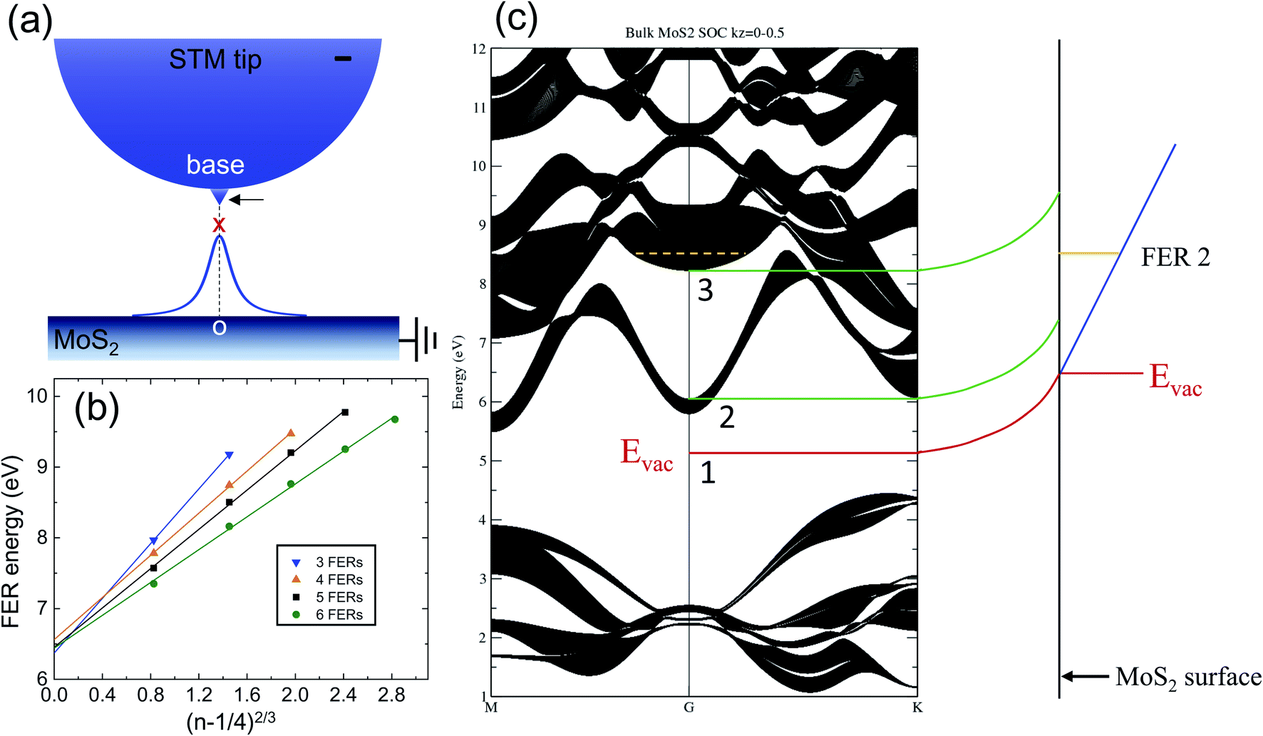
Fig. 2(a) illustrates that an STM tip mainly consists of a base with an effective radius (typically a few tens of nanometers) and a protrusion (marked by the arrow). The sharpness of an STM tip is determined by the open angle of the protrusion.24 According to electrostatics, the electric field in an STM junction is not constant due to the tip structure similar to that in Fig. 2(a). The field is the strongest at the tip but decays with distance from it.23 As a result, the external potential in the vacuum above the Fermi level of the tip is steeper than that below the Fermi level along the surface normal. The former determines the tunneling probability of an electron at the Fermi level in the field emission, corresponding to an average electric field FFE. The latter determines the number and energies of FERs, corresponding to an average electric field FFER. The tip sharpness leads to the FFE for field emission being stronger than the FFER for FERs,24 and a tip with higher sharpness can generate more FERs (see ESI note 4 for details†).
 |
| | Fig. 2 (a) Illustration of an STM tip consisting of a base with a radius typically tens of nanometers and a protrusion (marked by the arrow). The electric field for FERs appears at the dashed line normal to the surface from the o point to the classical turning point (cross) of the resonant electron. Because of this tip structure, the electric potential below the classical turning point has a distribution curve. (b) Energies of the higher-order peaks in Fig. 1(b)versus (n − 1/4)2/3, showing the linear relationship, from which the electric fields for generating FERs of different numbers and vacuum levels can be acquired. (c) Projected bulk band structure of MoS2 obtained by DFT calculation for energies ranging from 1 to 12 eV above the Fermi level. Line 1 indicates the vacuum level. Lines 2 and 3 mark the band edges of a band gap. The energy diagram on the right-hand side shows that due to band bending, the band edges and vacuum level in the bulk all move upward when approaching the surface. | |
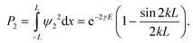
If an FER is a result of a quantized state in a triangular potential, then its energy En obeys35
| | 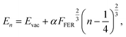 | (1) |
where
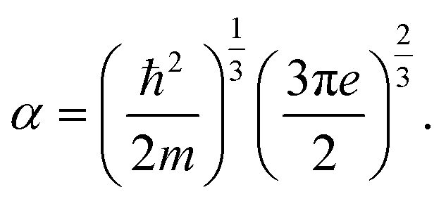
Evac is the vacuum level,
n = 1, 2, 3… is the quantum number, and
| | 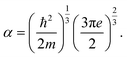 | (2) |
Fig. 2(b) shows plots of the energies of the higher-order peaks in Fig. 1(b)versus (n − 1/4)2/3. The results show that the data points in the cases of four, five, and six FERs can be fit well by the lines, indicating that eqn (1) is valid for higher-order peaks. From the line slope and the extrapolated value, one can obtain FFER and Evac, respectively. Fig. 2(b) reveals that a higher number of FERs corresponds to a weaker FFER. Therefore, the modulated linewidth originates from the variation in FFER.
3.2 Band bending in MoS2
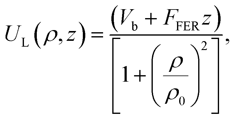
The FFER obtained from Fig. 2(b) appears at the dashed line normal to the surface in Fig. 2(a) from the surface (0 point) to the classical turning point (cross) of the resonant electron. Because MoS2 is a dielectric material with a dielectric constant of 3.7,36 the electric field can penetrate its surface to cause band bending in the interior.37 Thus, the electric potential along the surface normal is Vb + FFERz, where Vb is the potential of band bending and z is the distance from the surface. The electric potential UL below the classical turning point can be expressed as28| | 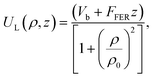 | (3) |
where ρ0 is a constant and ρ is the lateral distance from the dashed line, corresponding to the distribution curve in Fig. 2(a). Fig. 2(c) displays the projected bulk band structure of MoS2 obtained by DFT calculations38–42 for energies within the range of 1–12 eV above the Fermi level. The result shows that a band gap appears above the vacuum level (5.2 eV),43 which has band edges at 6.1 and 8.2 eV at the gamma point, marked by lines 2 and 3, respectively. Thus, the calculation result is consistent with the observation of the zero valley intensity in Fig. 1(a). However, the energy of FER 2 in Fig. 1(a) is 8.5 eV, outside of the band gap marked by the dashed line in Fig. 2(c). This inconsistency can be attributed to band bending because the vacuum level determined from the extrapolation in Fig. 2(b) is 6.45 eV for the case of five FERs. The potential energy of band bending is accordingly determined to be 1.25 eV (6.45 eV − 5.2 eV). The energy diagram on the right-hand side of Fig. 2(c) illustrates that the band edges and the vacuum level (line 1) in the bulk all move upward when approaching the surface due to band bending. Therefore, the band edges at the surface are 7.35 and 9.45 eV. Consequently, the energy of FER 2 is in the band gap, in agreement with the observation.
3.3 Potential well on the MoS2 surface under the STM tip
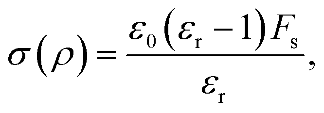
In addition to band bending, the penetration of the electric field can induce the positive polarization charge on the MoS2 surface. By using eqn (3), the electric field Fs(ρ) on the surface in the direction normal to the surface can be calculated as FFER/[1 + (ρ/ρ0)2]. Then, the density of the polarization charge σ(ρ) is calculated as| | 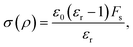 | (4) |
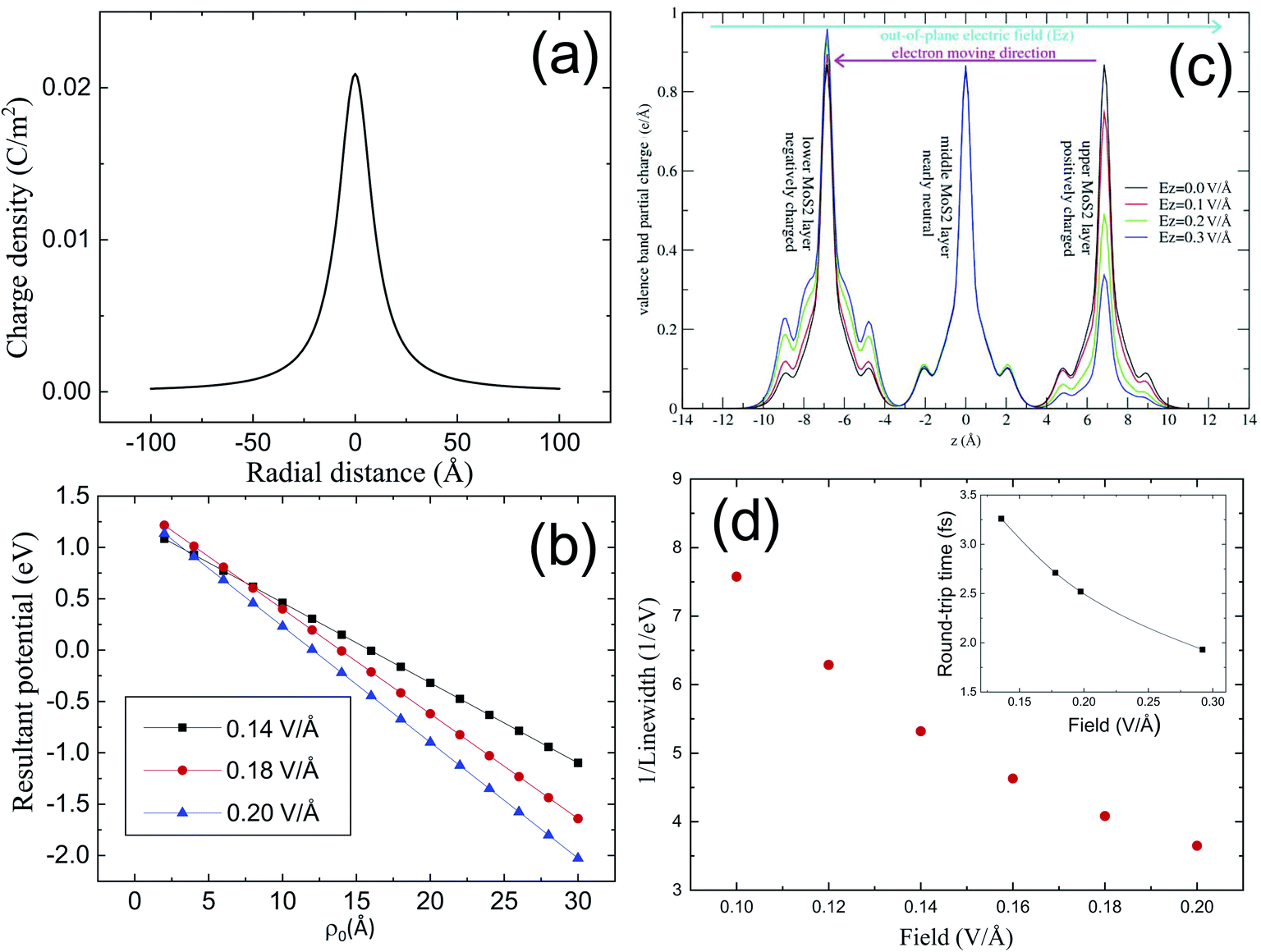
where εr is the dielectric constant of MoS2. Fig. 3(a) shows the calculated density distribution of the polarization charge, displaying that the density is highest at the center and decreases with ρ. An electron on the surface under the STM tip is repelled by the electric field in vacuum but is also simultaneously attracted by the polarization charge. Consequently, the electric potential on the surface is the superposition of UL(ρ, 0) and the potential Up(ρ) due to the polarization charge. Because UL and Up are both zero when ρ is infinite, whether the electron faces a potential well can be determined from the sign of the resultant potential Ur at the 0 point, that is, UL(0, 0) + Up(0). UL(0, 0) is the potential of band bending Vb, and Up(0) can be calculated as| | 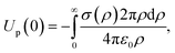 | (5) |
where ρ0 is the only parameter needed to calculate Ur. Fig. 3(b) shows Urversus ρ0 under the electric fields obtained from Fig. 2(b). The results indicate that Ur is negative for ρ0 greater than 18 Å. The parameter ρ0 is generally related to the tip base with an effective radius of tens of nanometers; therefore, it is plausible that ρ0 is greater than 18 Å. Accordingly, Ur is negative, and a potential well exists on the MoS2 surface beneath the STM tip. Moreover, Ur negatively increases with increasing FFER for the same ρ0, indicating that the depth of the potential well is deeper under a stronger FFER.
 |
| | Fig. 3 (a) Calculated density distribution of the polarization charge under an electric field of 0.18 V Å−1 and ρ0 = 10 Å, indicating that the density is the highest at the center and decreases with ρ. (b) Resultant potential Ur at the 0 point in Fig. 2(b)versus ρ0 under electric fields obtained from Fig. 2(a). (c) Charge profile of the valence band of the MoS2 slab under a uniform out-of-plane electric field ranging from 0.0 to 0.3 V Å−1. The external electric field significantly modifies the surface MoS2 trilayer valence charge profile. (d) The reciprocal of the FER linewidth of the first order versus the electric field, obtained from the calculation in ESI note 5.† Inset: RT time of a resonant electron in the STM junction versus the electric field obtained from Fig. 2(a). | |
Fig. 3(c) displays the calculated valence band partial charge profiles along the z-direction of the 3-layer MoS2 slab under a uniform out-of-plane electric field (Ez) ranging from 0.0 to 0.3 V Å−1. As clearly seen, the external electric field significantly modifies the surface MoS2 layer valence charge profile by pulling electrons from the upper MoS2 layer toward the lower MoS2 layer, keeping the middle MoS2 layer nearly neutral. As a result, the lower MoS2 layer is negatively charged, whereas the upper MoS2 layer is positively charged, consistent with our expectation. The electric field-induced electron transfer monotonically grows with increasing electric field strength, forming a mechanism for manipulating the width and depth of the potential well on the MoS2 surface via the electric field in the STM junction. We note here that the calculated charge density of the surface MoS2 layer is of the same order of magnitude as the maximum charge density estimated in Fig. 3(a).
3.4 Quantum trapping in one-dimensional square well
In the FER, resonant electrons move back and forth within a specific distance between the surface and the classical tuning point. Because En, FFER, and Evac are known, this distance s corresponding to FER can be calculated as (En − Evac)/eFFER. Consequently, the round-trip (RT) time t for resonant electron motion can be calculated from 2s = eFFERt2/m. The inset in Fig. 3(d) shows the RT time versus FFER in the case of FER 2, where the RT time is shown on the femtosecond scale. Previous studies have demonstrated that resonant electrons can emit light22,33 to become relaxed electrons with a lateral kinetic energy due to the inhomogeneous field in the STM junction;28 however, before relaxation, electrons should complete at least one RT to form the standing wave necessary to reveal the FER. Therefore, the RT time can basically reflect the lifetime of the resonant electrons. Thus, the inset in Fig. 3(d) indicates that the lifetime should monotonically decrease with increasing FFER, which can also be confirmed by exploiting the Fabry–Pérot mode2 to calculate the reciprocal of the FER linewidth of the first order without including the light emission and the band structure of the sample (see ESI note 5 for details†), as shown in Fig. 3(d). Fig. 3(d) is evidently contradictory to the observation in Fig. 1 that the linewidth modulates with FFER. The modulation range can be as large as one order of magnitude, implying that under a certain FFER, the lifetime can be substantially prolonged. Because the lifetime of a resonant electron terminates upon light emission, this significant extension of the lifetime indicates that resonant electrons cannot emit light to remain in FER for many more RTs. We suggest that the prohibition of light emission results from the same spin of the relaxed electron and the resonant electron as well as the Pauli exclusion principle.
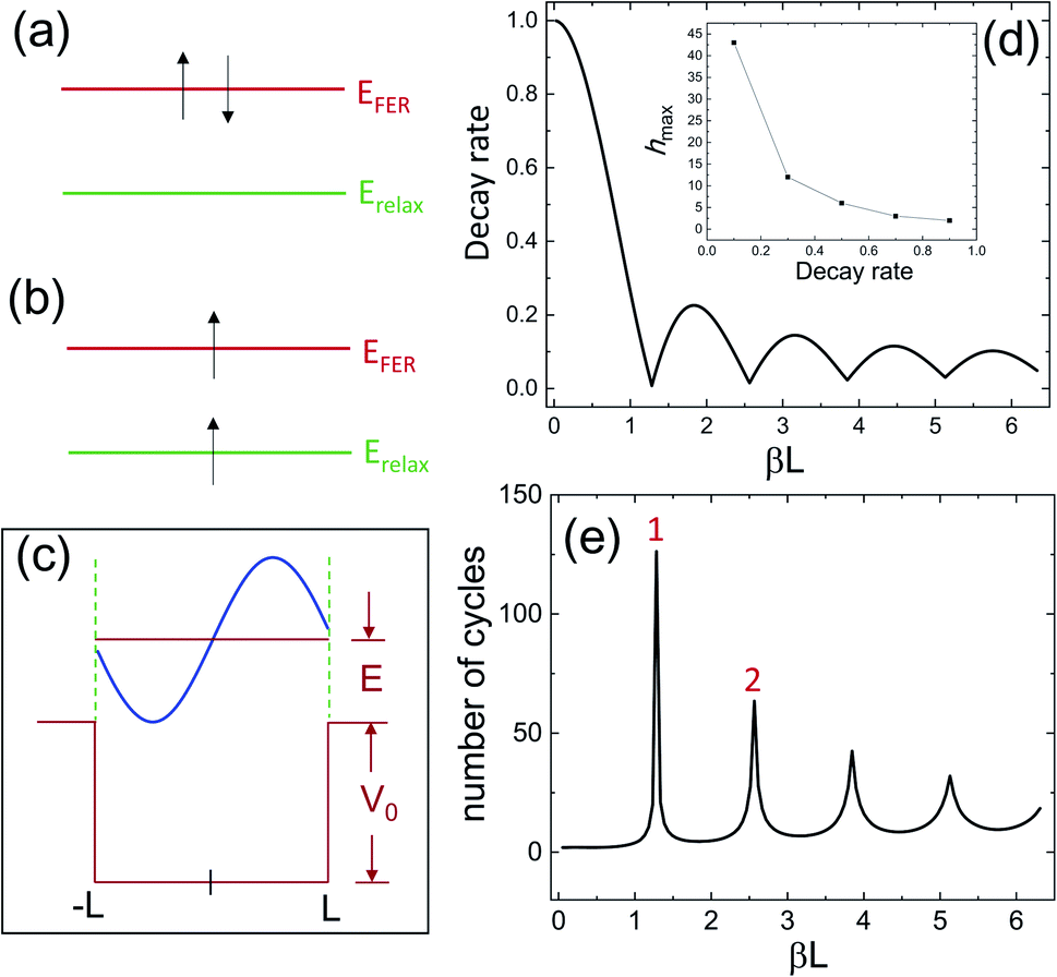
The linewidth of 12 meV corresponds to a lifetime of 27 fs if ΔEΔt = ħ/2. Therefore, the intervention of the Pauli exclusion principle requires a resonant electron and a relaxed electron to coexist on the femtosecond time scale. However, the set current in our experiment is 10 pA, which is equal to one electron per 16 ns. If electrons are emitted one by one every 16 ns, then two electrons cannot coexist on the femtosecond scale. In this context, we suggest that every 32 ns, two resonant electrons with opposite spins are successively emitted into the quantized state in the FER (Fig. 4(a)), which can occur through the exchange interaction (see ESI note 6 for details†). One resonant electron relaxes first through light emission and its spin should flip during relaxation to maximize the total spin according to Hund's rule. Consequently, the resonant electron and relaxed electron can simultaneously exhibit the same spin (Fig. 4(b)). The forbiddance of light emission from the resonant electron is accordingly established. The situation of the same spin in Fig. 4(b) is similar to the triplet excited state in phosphorescence.
 |
| | Fig. 4 (a) Two electrons with opposite spins are successively emitted into the quantized state in FER. (b) When one of the resonant electrons in (a) relaxes, its spin should be flipped to maximize the total spin according to Hund's rule. (c) One-dimensional square potential well with a width of 2L for modeling the quantum trapping, where the energy E of the relaxed electron in the well is higher than the well depth V0 and the wave function of the relaxed electron is a standing wave. (d) Decay rate of the probability versus βL, which is proportional to the size of the well, revealing local minima for E/V0 = 0.5 and γ = 0.003. Inset: Maximum number of cycles hmax for which the relaxed electron can remain in the well as a function of the decay rate for N = 100. (e) Average number of cycles versus βL showing an oscillatory feature; the maxima occur exactly at the minima of the decay rate in (d). | |
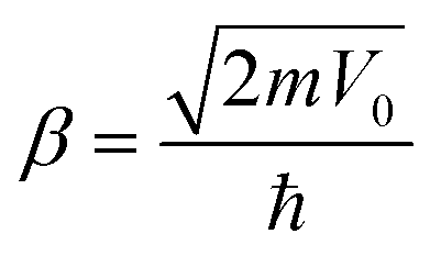
Because the resonant electrons are hot electrons, the lateral kinetic energy E of relaxed electrons is higher than the vacuum level of MoS2. Therefore, relaxed electrons in the potential well have energy higher than the well depth, which differs from the case of quantum confinement. One can expect that relaxed electrons are trapped such that they move back and forth in the well because of the formation of standing waves in the radial direction. However, these standing waves will dissipate because the wave function outside the well is a traveling wave instead of an evanescent wave. Therefore, relaxed electrons eventually leave the well. To model this case of quantum trapping, we assume that the potential well is a cylindrical well in which the radial wave function is a Bessel function of the first kind. We note that Bessel functions have oscillatory features similar to cosinusoidal and sinusoidal functions; this enables us to discuss quantum trapping by using a one-dimensional square well with depth V0 and width 2L, as depicted in Fig. 4(c). The wave vector k of the relaxed electrons in the well satisfies
| | 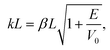 | (6) |
where

. The formation of standing waves requires the relaxed electrons to be reflected at −
L and
L so that they go through a complete cycle in the square well. If the energy of relaxed electrons is much higher than the well depth (
E ≫
V0), then these electrons behave similarly to classical particles and leave the well without reflection. Accordingly, the wave function of relaxed electrons after the first cycle can be
| | 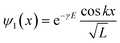 | (7) |
or
| | 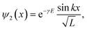 | (8) |
where
γ is a constant. The exponential term can satisfy no standing wave for
E ≫
V0 because
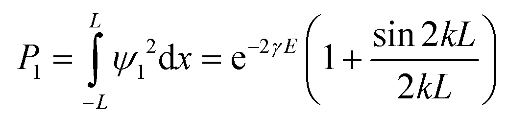
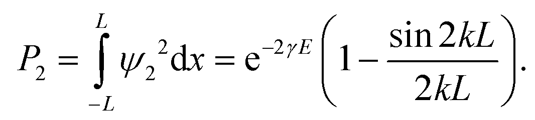
E can be considered infinite under this condition. Thus, the probability in the well is
| |  | (9) |
or
| |  | (10) |
when
E = 0 and 0 < 2
kL < π, sin
![[thin space (1/6-em)]](https://www.rsc.org/images/entities/char_2009.gif)
2
kL is positive, and thus
P1 > 1 and
P2 < 1. Because the probability should not be greater than 1, the wave function is
ψ2(
x) in this case. Similarly, the wave function is
ψ1(
x) when
E = 0 and π < 2
kL < 2π.
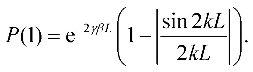
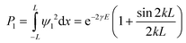
The results in Fig. 3(b) indicate that V0 and β can increase with FFER. Moreover, the area with polarization charges is larger under a stronger FFER. Hence, L is wider when FFER is higher. Consequently, the well size 2LV0 can be tuned by FFER. Based on eqn (3), the electrostatic force in the radial direction enhances with FFER, causing E to also increase with FFER. Therefore, it is plausible to calculate the probability under the conditions that E/V0 is a constant independent of FFER and E is replaced with βL. By combining eqn (9) and (10), the probability P(1) that a relaxed electron exists in the well after the first cycle can be expressed as
| | 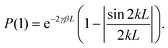 | (11) |
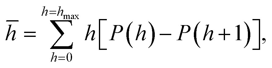
Therefore, the probability of leaving the well is 1 − P(1), which can be viewed as the decay rate R of the probability. Accordingly, the probability that a relaxed electron stays in the well for h cycles is
From eqn (12), we know that the probability that a relaxed electron has remained in the well for (h − 1) cycles but leaves the well in the hth cycle is P(h − 1) − P(h). As a result, the average number of cycles ![[h with combining macron]](https://www.rsc.org/images/entities/i_char_0068_0304.gif) of all relaxed electrons is
of all relaxed electrons is
| |  | (13) |
where
hmax is the maximum number of cycles for which a relaxed electron can remain, which depends on the number
N of all relaxed electrons when observing the FER.
Eqn (11) indicates that P(1) depends only on βL; this enables us to show the decay rate versus βL. Fig. 4(d) demonstrates that the decay rate varies with βL in oscillation, and a local minimum appears when 2kL equals an integral multiple of π. The manifestation of local minima is due to the transition of the wave function. The inset in Fig. 4(d) shows hmax as a function of the decay rate, revealing that hmax increases with decreasing decay rate. Consequently, when the decay rate is lower, the average number of cycles should be higher because relaxed electrons can remain in the well for more cycles. We use the results in Fig. 4(d) and eqn (12) and (13) to calculate the average number of cycles versus βL. Fig. 4(e) shows that oscillates with βL, and the maxima occur exactly at the minima of the decay rate. In addition, is insensitive to N.
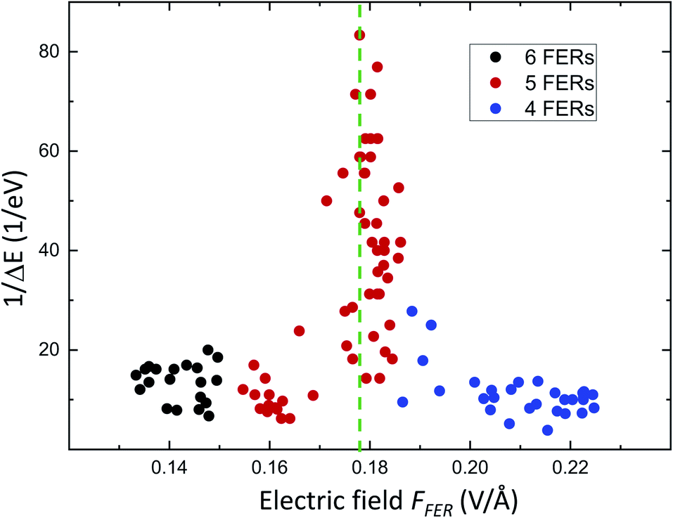
The time per cycle, equal to 4L/(ħk/m), is proportional to L/β. Because both β and L increase with FFER, it is plausible that the cycle time is independent of FFER. Because βL is proportional to the well size, Fig. 4(e) can be interpreted as evidence that the mean duration for which the square well traps relaxed electrons oscillates with the well size. For certain sizes, the mean trapping time (MTT) is much longer, manifesting resonance trapping. The MTT can change by up to one order of magnitude at the first and second resonances marked by 1 and 2 in Fig. 4(e), respectively. Evidently, the variation in the linewidths in Fig. 1(c)–(f) has the characteristics of quantum trapping, leading us to suggest that the lifetime of a resonant electron is governed by the relaxed electron through the Pauli exclusion principle. Thus, the MTT is recorded in the linewidth of the FER. The narrow linewidths of 12 meV and 16 meV in Fig. 1(d) and (f), respectively, result from the relaxed electrons engaging in resonance trapping. Broad FERs indicate low MTT in quantum trapping. Due to quantum trapping, the lifetimes of paired resonant electrons in Fig. 4(a) can be different. The variation in the FER linewidth is mainly determined by the mean lifetime of resonant electrons relaxing subsequently. Moreover, we have also accumulated sufficient spectra with four, five and six FERs to plot the reciprocal of the linewidth versus FFER to display resonance trapping, as shown in Fig. 5. The plot displays that FFER could be gradually increased from 0.13 to 0.23 V Å−1. The plot depicts the characteristics of a narrow peak, which are highly similar to the peak of resonance trapping in Fig. 4(e). Therefore, Fig. 5 demonstrates that the resonance trapping only appeared under a certain FFER, which is 0.178 V Å−1 (marked by a dashed line). However, at approximately 0.178 V Å−1, several data points still appear with values are close to those at 0.14 and 0.22 V Å−1. Fig. 4(e) displays that the resonance trapping is highly sensitive to the size of the potential well. Therefore, the appearance of these data points indicates that even when the electric fields are near 0.178 V Å−1, their corresponding tip structures may induce potential wells with sizes that deviate slightly from those for resonance trapping, causing a low 1/ΔE. In addition, the data points in Fig. 5 are colored in terms of the number of FERs. It is clear that the high values of 1/ΔE appear at 5 FERs, whereas the values of 1/ΔE are low for 4 and 6 FERs.
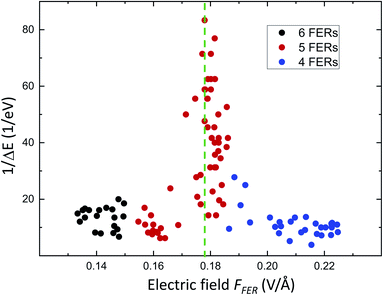 |
| | Fig. 5 Plot of 1/ΔE versus FFER, in which the data points are accumulated from 108 spectra with four, five, and six FERs. | |
4. Conclusions
In summary, we discover that the linewidth of the FER is a meaningful quantity that is not only associated with the lifetime of a resonant electron but is also able to store information regarding the behavior of relaxed electrons. The delivery of information occurs through the action of the Pauli exclusion principle. In this study, when the size of the potential well on the MoS2 surface situates the relaxed electrons in resonance trapping, the resonant electrons can receive this information such that their lifetimes are considerably extended. Therefore, ultra-narrow FERs are manifested. Furthermore, the potential well induced by the STM tip should be generally formed on the surfaces of different materials, implying that the phenomenon of quantum trapping can be universally observed. The variation in the well size with the electric field may depend on the dielectric properties of the materials. Therefore, quantum trapping manifested in the STM configuration can be developed as a new technique for probing dielectric properties on the nanometer scale.
Conflicts of interest
There are no conflicts to declare.
Acknowledgements
The authors acknowledge T. K. Lee for helpful discussions. This work was supported by the Ministry of Science and Technology (grant numbers: MOST 106-2112-M-001-004-MY3 and MOST 106-2112-M-007-012-MY3) and Academia Sinica (grant numbers: AS-iMATE-107-11 and AS-105-TP-A03), Taiwan. H. T. J. also thanks the CQT-NTHU-MOE, NCHC and CINC-NTU, Taiwan for technical support.
References
- I. B. Altfeder, K. A. Matveev and D. M. Chen, Electron fringes on a quantum wedge, Phys. Rev. Lett., 1997, 78, 2815–2818 CrossRef CAS.
- J. J. Paggel, T. Miller and T. C. Chiang, Quantum-well states as Fabry-Perot modes in a thin-film electron interferometer, Science, 1999, 283, 1709–1711 CrossRef CAS.
- M. Becker and R. Berndt, Scattering and lifetime broadening of quantum well states in Pb films on Ag(111), Phys. Rev. B: Condens. Matter Mater. Phys., 2010, 81, 205438 CrossRef.
- D. Wegner, A. Bauer and G. Kaindl, Electronic structure and dynamics of quantum-well states in thin Yb metal films, Phys. Rev. Lett., 2005, 94, 126804 CrossRef CAS.
- M. C. Yang, C. L. Lin, W. B. Su, S. P. Lin, S. M. Lu, H. Y. Lin, C. S. Chang, W. K. Hsu and T. T. Tsong, Phase Contribution of image potential on empty quantum well states in Pb islands on the Cu(111) surface, Phys. Rev. Lett., 2009, 102, 196102 CrossRef CAS.
- J. Kim, S. Qin, W. Yao, Q. Niu, M. Y. Chou and C. K. Shih, Quantum size effects on the work function of metallic thin film nanostructures, Proc. Natl. Acad. Sci. U. S. A., 2010, 107, 12761–12765 CrossRef CAS.
- W. Y. Chan, H. S. Huang, W. B. Su, W. H. Lin, H. T. Jeng, M. K. Wu and C. S. Chang, Field-induced expansion deformation in Pb Islands on Cu(111): evidence from energy shift of empty quantum-well states, Phys. Rev. Lett., 2012, 108, 146102 CrossRef CAS.
- J. A. Kubby, Y. R. Wang and W. J. Greene, Electron interferometry at a heterojunction interface, Phys. Rev. Lett., 1990, 65, 2165 CrossRef CAS.
- W. F. Chung, Y. J. Feng, H. C. Poon, C. T. Chan, S. Y. Tong and M. S. Altman, Layer spacings in coherently strained epitaxial metal films, Phys. Rev. Lett., 2003, 90, 216105 CrossRef CAS.
- W. B. Su, S. M. Lu, C. L. Jiang, H. T. Shih, C. S. Chang and T. T. Tsong, Stark shift of transmission resonance in scanning tunneling spectroscopy, Phys. Rev. B: Condens. Matter Mater. Phys., 2006, 74, 155330 CrossRef.
- G. Binnig, K. H. Frank, H. Fuchs, N. Garcia, B. Reihl, H. Rohrer, F. Salvan and A. R. Williams, Tunneling spectroscopy and inverse photoemission - image and field states, Phys. Rev. Lett., 1985, 55, 991–994 CrossRef CAS.
- R. S. Becker, J. A. Golovchenko and B. S. Swartzentruber, Electron interferometry at crystal-surfaces, Phys. Rev. Lett., 1985, 55, 987–990 CrossRef CAS.
- K. H. Gundlach, Zur Berechnung Des Tunnelstroms Durch Eine Trapezformige Potentialstufe, Solid-State Electron., 1966, 9, 949–957 CrossRef.
- C. L. Lin, S. M. Lu, W. B. Su, H. T. Shih, B. F. Wu, Y. D. Yao, C. S. Chang and T. T. Tsong, Manifestation of work function difference in high order Gundlach oscillation, Phys. Rev. Lett., 2007, 99, 216103 CrossRef CAS.
- H. S. Huang, W. Y. Chan, W. B. Su, G. Hoffmann and C. S. Chang, Measurement of work function difference between Pb/Si(111) and Pb/Ge/Si(111) by high-order Gundlach oscillation, J. Appl. Phys., 2013, 114, 214308 CrossRef.
- F. Schulz, R. Drost, S. K. Hämäläinen, T. Demonchaux, A. P. Seitsonen and P. Liljeroth, Epitaxial hexagonal boron nitride on Ir(111): A work function template, Phys. Rev. B: Condens. Matter Mater. Phys., 2014, 89, 235429 CrossRef.
- Z. Li, H. Y. Chen, K. Schouteden, E. Janssens, C. Van Haesendonck, P. Lievens and G. Pacchioni, Spontaneous doping of two-dimensional NaCl films with Cr atoms: aggregation and electronic structure, Nanoscale, 2015, 7, 2366 RSC.
- K. Schouteden, B. Amin-Ahmadi, Z. Li, D. Muzychenko, D. Schryvers and C. Van Haesendonck, Electronically decoupled stacking fault tetrahedra embedded in Au(111) films, Nat. Commun., 2016, 7, 14001 CrossRef CAS.
- C. Gutiérrez, L. Brown, C. J. Kim, J. Park and A. N. Pasupathy, Klein tunneling and electron trapping in nanometre-scale graphene quantum dots, Nat. Phys., 2016, 12, 3806 Search PubMed.
- Q. Zhang, J. Yu, P. Ebert, C. Zhang, C. R. Pan, M. Y. Chou, C. K. Shih, C. Zeng and S. Yuan, Tuning Band gap and work function modulations in monolayer hBN/Cu(111) heterostructures with moire patterns, ACS Nano, 2018, 12, 9355 CrossRef CAS.
- W. B. Su, S. M. Lu, C. L. Lin, H. T. Shih, C. L. Jiang, C. S. Chang and T. T. Tsong, Interplay between transmission background and Gundlach oscillation in scanning tunneling spectroscopy, Phys. Rev. B: Condens. Matter Mater. Phys., 2007, 75, 195406 CrossRef.
- J. Martínez-Blanco and S. Fölsch, Light emission from Ag(111) driven by inelastic tunneling in the field emission regime, J. Phys.: Condens. Matter, 2015, 27, 255008 CrossRef.
- W. Y. Chan, S. M. Lu, W. B. Su, C. C. Liao, G. Hoffmann, T. R. Tsai and C. S. Chang, Sharpness-induced energy shifts of quantum well states in Pb islands on Cu(111), Nanotechnol, 2017, 28, 095706 CrossRef.
- S. M. Lu, W. Y. Chan, W. B. Su, W. W. Pai, H. L. Liu and C. S. Chang, Characterization of external potential for field emission resonances and its applications on nanometer-scale measurements, New J. Phys., 2018, 20, 043014 CrossRef.
- W. B. Su, C. L. Lin, W. Y. Chan, S. M. Lu and C. S. Chang, Field enhancement factors and self-focus functions manifesting in field emission resonances in scanning tunneling microscopy, Nanotechnol, 2016, 27, 175705 CrossRef.
- K. Bobrov, A. J. Mayne and G. Dujardin, Atomic-scale imaging of insulating diamond through resonant electron injection, Nature, 2001, 413, 616–619 CrossRef CAS.
- S. Liu, M. Wolf and T. Kumagai, Plasmon-assisted resonant electron tunneling in a scanning tunneling microscope junction, Phys. Rev. Lett., 2018, 121, 226802 CrossRef CAS.
- J. I. Pascual, C. Corriol, G. Ceballos, I. Aldazabal, H. P. Rust, K. Horn, J. M. Pitarke, P. M. Echenique and A. Arnau, Role of the electric field in surface electron dynamics above the vacuum level, Phys. Rev. B: Condens. Matter Mater. Phys., 2007, 75, 165326 CrossRef.
- P. Wahl, M. A. Schneider, L. Diekhoner, R. Vogelgesang and K. Kern, Quantum coherence of image-potential states, Phys. Rev. Lett., 2003, 91, 106802 CrossRef CAS.
- K. Schouteden and C. Van Haesendonck, Quantum confinement of hot image-potential state electrons, Phys. Rev. Lett., 2009, 103, 266805 CrossRef CAS.
- S. Stepanow, A. Mugarza, G. Ceballos, P. Gambardella, I. Aldazabal, A. G. Borisov and A. Arnau, Localization, splitting, and mixing of field emission resonances induced by alkali metal clusters on Cu(100), Phys. Rev. B: Condens. Matter Mater. Phys., 2011, 83, 115101 CrossRef.
- F. Craes, S. Runte, J. Klinkhammer, M. Kralj, T. Michely and C. Busse, Mapping Image Potential States on Graphene Quantum Dots, Phys. Rev. Lett., 2013, 111, 056804 CrossRef.
- J. Coombs, J. Gimzewski, B. Reihl, J. Sass and R. Schlittler, Photon emission experiments with the scanning tunneling microscope, J. Microsc., 1988, 152, 325 CrossRef CAS.
- S. Schuppler, N. Fischer, Th. Fauster and W. Steinmann, Lifetime of image-potential states on metal surfaces, Phys. Rev. B: Condens. Matter Mater. Phys., 1992, 46, 13539 CrossRef CAS.
-
J. J. Sakurai, Modern Quantum Mechanics, Benjamin-Cummings, New York, 1st edn, 1985, p. 104 Search PubMed.
- C. P. Lu, G. Li, K. Watanabe, T. Taniguchi and E. Y. Andrei, MoS2: choice substrate for accessing and tuning the electronic properties of graphene, Phys. Rev. Lett., 2014, 113, 156804 CrossRef.
- R. M. Feenstra, Y. Dong, M. P. Semtsiv and W. T. Masselink, Influence of tip-induced band bending on tunneling spectra of semiconductor surfaces, Nanotechnol, 2016, 18, 044015 CrossRef.
- G. Kresse and J. Furthmuller, Efficiency of ab initio total energy calculations for metals and semiconductors using a plane-wave basis set, Comput. Mater. Sci., 1996, 6, 15–50 CrossRef CAS.
- G. Kresse,
Ab initio molecular dynamics for liquid metals, J. Non-Cryst. Solids, 1995, 192–193, 222–229 CrossRef.
- G. Kresse and J. Furthmuller, Efficient iterative schemes for ab initio total-energy calculations using a plane-wave basis set, Phys. Rev. B: Condens. Matter Mater. Phys., 1996, 54, 11169–11186 CrossRef CAS.
- J. P. Perdew, J. A. Chevary, S. H. Vosko, K. A. Jackson, M. R. Pederson, D. J. Singh and C. Fiolhais, Atoms, molecules, solids, and surfaces: applications of the generalized gradient approximation for exchange and correlation, Phys. Rev. B: Condens. Matter Mater. Phys., 1992, 46, 6671–6687 CrossRef CAS.
- J. P. Perdew and Y. Wang, Pair-distribution function and its coupling-constant average for the spin-polarized electron-gas, Phys. Rev. B: Condens. Matter Mater. Phys., 1992, 46, 12947–12954 CrossRef.
- I. Popov, G. Seifert and D. Tomanek, Designing electrical contacts to MoS2 monolayers: a computational study, Phys. Rev. Lett., 2012, 108, 156802 CrossRef.
Footnote |
| † Electronic supplementary information (ESI) available. See DOI: 10.1039/d0na00682c |
|
| This journal is © The Royal Society of Chemistry 2020 |
Click here to see how this site uses Cookies. View our privacy policy here. 
 Open Access Article
 This Open Access Article is licensed under a Creative Commons Attribution-Non Commercial 3.0 Unported Licence
 *a,
Shin-Ming
Lu
*a,
Shin-Ming
Lu


 . The formation of standing waves requires the relaxed electrons to be reflected at −L and L so that they go through a complete cycle in the square well. If the energy of relaxed electrons is much higher than the well depth (E ≫ V0), then these electrons behave similarly to classical particles and leave the well without reflection. Accordingly, the wave function of relaxed electrons after the first cycle can be