
 Open Access Article
 This Open Access Article is licensed under a Creative Commons Attribution-Non Commercial 3.0 Unported Licence
Single-nanostructure bandgap engineering enabled by magnetic-pulling thermal evaporation growth
Jinyou
Xu
 *,
Xingyu
Wang
and
Richard
Nötzel
*
*,
Xingyu
Wang
and
Richard
Nötzel
*
Guangdong Provincial Key Laboratory of Optical Information Materials and Technology, Institute of Electronic Paper Displays, National Center for International Research on Green Optoelectronics, South China Academy of Advanced Optoelectronics, South China Normal University, Guangzhou 510006, People's Republic of China. E-mail: jinyou.xu@m.scnu.edu.cn; richard.noetzel@scnu.edu.cn
First published on 7th August 2020
Abstract
Realizing the substantial potential of bottom-up 1D semiconductor nanostructures in developing functional nanodevices calls for dedicated single-nanostructure bandgap engineering by various growth approaches. Although thermal evaporation has been advised as a facile approach for most semiconductors to form 1D nanostructures from bottom-up, its capability of achieving single-nanostructure bandgap engineering was considered a challenge. In 2011, we succeeded in the direct growth of composition-graded CdS1−xSex (0 ≤ x ≤ 1) nanowires by upgrading the thermal-evaporation tube furnace with a home-made magnetic-pulling module. This report aims to provide a comprehensive review of the latest advances in the single-nanostructure bandgap engineering enabled by the magnetic-pulling thermal evaporation growth. The report begins with the description of different magnetic-pulling thermal evaporation strategies associated with diverse examples of composition-engineered 1D nanostructures. Following is an elaboration on their optoelectronic applications based on the resulting single-nanostructure bandgap engineering, including monolithic white-light sources, proof-of-concept asymmetric light propagation and wavelength splitters, monolithic multi-color and white-light lasers, broadband-response photodetectors, high-performance transistors, and recently the most exciting single-nanowire spectrometer. In the end, this report concludes with some personal perspectives on the directions toward which future research might be advanced.
 Jinyou Xu | Jinyou Xu received a B.S. in Applied Physics (2008) and a PhD in Materials Science and Engineering (2014, with Prof. Anlian Pan) from Hunan University. He was a postdoctoral fellow (with Prof. Ernesto Joselevich) in the Department of Materials and Interfaces at Weizmann Institute of Science from 2014 to 2018. Since 2019, he has been a professor of Materials Physics at the South China Academy of Advanced Optoelectronics in South China Normal University. His current research focuses on bottom-up one-dimensional semiconductor nanostructures, with major interest in their orientated growth, composition engineering, and scale-up fabrication of optoelectronic devices. |
 Xingyu Wang | Xingyu Wang received his B.S. degree from the Department of Materials Science and Engineering at Lanzhou Tech University in 2015. Since 2017, he has been a PhD candidate (with Prof. Richard Nötzel) at the South China Academy of Advanced Optoelectronics in South China Normal University. His main research interests include the guided growth of 1D semiconductor nanostructures on patterned substrates and their applications in optoelectronics. |
 Richard Nötzel | Richard Nötzel received Diploma in Physics from the Technical University of Munich in 1989. From 1990 he stayed at the Max Planck Institute for Solid State Research in Stuttgart and received the doctoral degree in 1992. After working in Japan, Germany, The Netherlands, Spain and Italy, he joined the South China Normal University in 2017 as full professor. His work includes the direct growth of nanostructured semiconductors for optoelectronic and electrochemical devices. For his research he received the Otto Hahn Medal of the Max-Planck Society, the NTT research award, and the Academy Award of the Berlin-Brandenburg Academy of Science. |
1. Introduction
1D semiconductor nanostructures (wires, belts, tubes) have been recognized as a more flexible choice than epitaxial thin films in terms of developing composition-engineered semiconductors with new or even tunable bandgaps owing to their higher tolerance of lattice mismatch between dissimilar semiconductors or between target nanostructures and supporting substrates.1–6 Moreover, 1D semiconductor nanostructures provide a class of versatile building blocks for “bottom-up” construction of nanoscale devices and systems7–10—which are emerging as promising alternatives for further miniaturization of electronic circuitry and its components in the future, even though conventional “top-down” microfabrication employing photolithography continues to be the most prevalent technique at present. Realizing the substantial potential of bottom-up 1D nanostructures for the development of functional nanodevices, however, requires a predictable control over their composition, bandgap, interface, and alignment. In particular, one of the urgent tasks is to achieve various composition/bandgap engineering within single 1D nanostructures (hereafter referred to as “single-nanostructure composition/bandgap engineering”). For example, composition-graded nanowires (Fig. 1a and b) enable a package of abundant tuneable bandgaps in an ultra-compact volume, therefore they can serve as wavelength-integrated nanoscale light sources.11,12 Axial hetero-nanowires (Fig. 1c) with a type-II energy band diagram have been suggested as a promising structure for nanoscale light-emitting diodes.13 Radial hetero-nanowires (Fig. 1d) with abruptly changed bandgaps along the nanowire radial axis provide an ideal configuration for the implementation of microscale photovoltaic cells since the coaxial structure resolves the mismatch between the shorter length scale for minority carrier diffusion and the longer length scale for light absorption by decoupling these directions.14 Lateral hetero-nanobelts (Fig. 1e) and composition-graded nanobelts (Fig. 1f) not only deliver abruptly and gradually changed bandgaps along the nanobelt width direction for broadband-response photodetectors but also provide a class of novel parallel optical cavities for monolithic multi-color lasers.15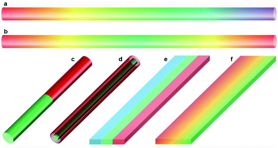 | ||
| Fig. 1 Schematic drawings of various composition-engineered 1D semiconductor nanostructures. Alloy nanowires with (a) a single composition gradient and (b) dual symmetrical composition gradients along the length axis. (c) Axial hetero-nanowires. (d) Radial hetero-nanowires. (e) Multi-lane lateral hetero-nanobelts. (f) Alloy nanobelts with a composition gradient along the width direction. | ||
To date, significant progress has been made in the growth of composition-engineered 1D nanostructures based on a number of bottom-up approaches. For instance, the hybrid pulsed laser ablation/chemical vapor deposition (LA-CVD) process enabled the block-by-block growth of single-crystalline Si/SiGe,16 GaAs/GaP, n-Si/p-Si and n-InP/p-InP superlattice nanowires.17 Metal–organic chemical vapor deposition (MOCVD) has been successfully employed for the growth of multi-quantum-well core/shell nanowire heterostructures,18 axial hybrid III–V/silicon nanowires,19 and so on. Molecular beam epitaxy (MBE) has been adopted for the growth of n-GaN/InGaN/p-GaN p–i–n hetero-nanowires,20 GaAs/InAs core–shell nanowires,21 near full-composition GaAs1−xSbx nanowires,22 composition-graded InGaAs23 and InGaN24 nanowires, GaN/AlxGa1−xN nanowires with embedded GaN nano-discs,25 and so on. Atomically abrupt Si–Ge axial hetero-nanowires were synthesized in a solvent vapor growth system26,27 and inside a transmission electron microscope (TEM).28 At present, MOCVD and MBE are still the limited and optimal solutions for those applications which require sub-monolayer growth control and atomically sharp interfaces,29 although their success generally relies on costly instruments and sophisticated handling skills.
In contrast to the MOCVD and MBE growth, thermal evaporation provides a facile and cost-effective solution for semiconductors to form 1D nanostructures from bottom up by evaporating their bulk counterparts on the basis of the metal-catalytic vapor–liquid–solid (VLS)30 or the non-catalytic vapor–solid (VS) mechanisms.31 To this end, the generality of thermal evaporation growth has been well proven with a growing list of 1D semiconductor nanostructures, including most II–VI and III–V semiconductors and their alloys,9,32–39 oxide semiconductors,40,41 perovskites,42,43 small-molecular organic semiconductors,44 and so on. However, while having advantages of economical apparatus and simple handling skills, thermal evaporation growth was once considered very challenging in terms of achieving single-nanostructure composition engineering owing to the difficulty in adjusting the evaporating sources (or substrates), which are pre-sealed in the tube reactor during growth. In order to address this issue, we integrated a home-made magnetic pulling module into a conventional tube furnace in 2011, accordingly achieving an in situ “source-moving” process by driving the magnet outside the tube during the growth. With this source-moving strategy, we succeeded in the direct growth of composition-graded CdS1−xSex (0 ≤ x ≤ 1) alloy nanowires for the first time.11 Thereafter, the magic box of single-nanostructure bandgap engineering enabled by the magnetic-pulling thermal evaporation growth was opened and a growing list of composition-engineered 1D nanostructures12,15,45–50 was synthesized, providing diverse single-nanostructure bandgap engineering for a large variety of nano-optoelectronics. In this report, we aim to provide readers an overview of the recent advances in single-nanostructure bandgap engineering enabled by magnetic-pulling thermal evaporation growth over the past decade. Although significant similar progress has been achieved as well based on the MBE and MOCVD growth, as mentioned above, here we will not include such progress in view of the scope of this review.
2. Composition-graded alloy nanowires
The concept of compositional gradient of semiconductors dates back to the 1960s, when bulk single crystals of II–VI semiconductors with graded-bandgaps were prepared by two different vapor-phase methods with constant and variable charge temperatures,51–54 respectively. Later, this concept was extended to the nanoscience research community and a large number of 1D semiconductor nanostructures with graded compositions on a single substrate were grown with the assistance of temperature gradients of the heating apparatus,2,55 or spatial source reagent gradients1,56 or both,57 such as ZnxCd1−xS,3 CdSxSe1−x,2,55 InGaN,56 ZnyCd1−ySxSe1−x,1,57 ConSi,58 ZnxCd1−xSe,59 ZnxCd1−xTe,60,61 GaZnSeAs,62 InAsxP1−x,63 and CdxPb1−xS64 graded alloy nanostructures on single centimeter-scale substrates. The alloy composition between adjacent nanostructures on the same substrate is continuously varied over a wide range along a certain direction of the substrate, a concept of single-chip graded bandgap engineering which was firstly proposed by Pan et al.55 However, the composition of individual nanostructures remained at a certain stoichiometric ratio, which means no monolithic graded bandgaps within a single 1D nanostructure were achieved. In this part, we will only review the progress in single-nanostructure graded bandgap engineering as the space here is limited. For more information on single-chip graded bandgap engineering, please refer to the review contributed by Zhuang et al. in 2012.5Unlike the impressive progress made in single-chip graded bandgap engineering, the progress in single-nanostructure graded bandgap engineering is still limited and only a few examples have been reported so far.20,65–68 Dong et al. observed a composition-graded ZnSexTe1−x segment in ZnSe–ZnTe hetero-nanowires generated by a solution–liquid–solid (SLS) growth mechanism.65 Composition-graded NiSi nanowires were synthesized through a spontaneous chemical vapor growth.68 Plasma-assisted MBE enabled the growth of composition-graded InGaAs23 and InGaN24 nanowires as well as sandwich-like n-GaN/InGaN/p-GaN p–i–n hetero-nanowires with an indium composition gradient in the InGaN segments.20 Axially graded Si1−xGex nanowires reported by Yang and co-workers were fabricated by the kinetic control of the Au-catalytic decomposition of the precursors during chemical vapor synthesis.66,69,70 Composition-graded CuSi nanorod arrays with poor morphology and quality were synthesized by an oblique angle co-deposition technique.67 In fact, none of these examples stemmed from conventional thermal evaporation growth before our pioneering work on composition-graded CdS1−xSex nanowires,11 to the best of our knowledge. In 2011, our group and collaborators developed the first in situ “source-moving” thermal evaporation strategy by incorporating a home-made magnetic-pulling module into a conventional tube furnace, and accordingly achieved the growth of composition-graded CdS1−xSex nanowires, in which the S/Se elemental ratio (x) increased gradually from 0 on one end to 1 on the opposite end of the nanowires.11 Thereafter, we further proposed a “substrate-moving” thermal evaporation strategy for the growth of composition-graded ZnyCd1−ySxSe1−x (0 ≤ x, y ≤ 1) quaternary alloy nanowires with the assistance of a similar magnetic pulling module.12 On the basis of these composition-graded nanowires, novel single-nanostructure graded bandgap engineering is achieved via the facile thermal evaporation growth for the first time.
2.1 Source-moving strategy
The source-moving setup consists of a horizontal tube furnace and a home-made magnetic source-pulling module, as shown schematically in Fig. 2a. Therefore, the solid reagents pre-sealed inside the quartz tube (“source”) can be moved into/out of the heating zone on demand during high-temperature growth by driving the external magnet. For example, the evaporation rate of CdS (CdSe) powders in Fig. 2a is expected to decrease (increase) gradually by pushing the external magnet to the right side at a selected slow speed as a result of the symmetrical temperature gradient from the furnace center to its two ends. The changed evaporation rates of CdS and CdSe powders would deliver a gradually changed S/Se vapor ratio inside the tube, eventually leading to the growth of composition-graded CdS1−xSex nanowires on the Au-coated substrate via the well-known VLS mechanism.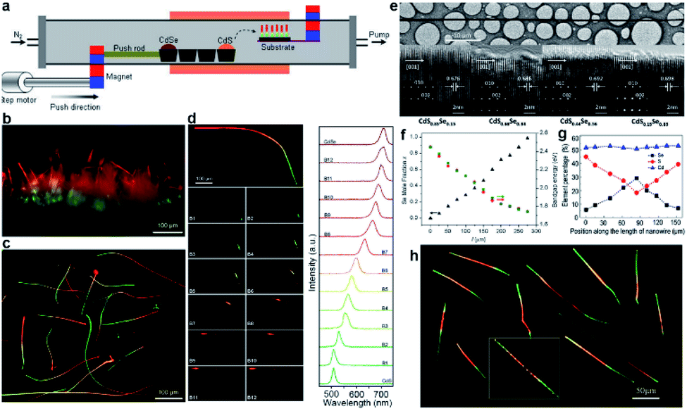 | ||
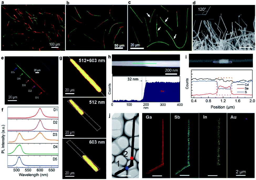
| Fig. 2 Composition-graded CdS1−xSex (0 ≤ x ≤ 1) ternary alloy nanowires. (a–f) CdS1−xSex nanowires with a single composition gradient: (a) schematic diagram of source-moving thermal evaporation growth; real-color optical photograph of (b) as-grown and (c) dispersed graded nanowires; (d) spatially resolved PL emission and corresponding spectra from a single graded nanowire; (e) TEM characterization; (f) position-dependent Se molar fractions and bandgaps. (g and h) CdS1−xSex nanowire with symmetric dual composition gradients: (g) position-dependent molar fractions; (h) real-color optical photograph of dispersed nanowires. (a–f) Reproduced with permission.11 Copyright 2011, American Chemical Society. (g and h) Reproduced with permission.46 Copyright 2013, American Chemical Society. | ||
Under illumination of a dispersive 405 nm laser, the emission color of each nanowire changes continuously from green at one end, through yellow and orange in the middle, to red at the other end (Fig. 2b and c), indicating a gradually varied chemical composition. Fig. 2d further shows that different emission colors can be extracted from different locations when the nanowire is locally illuminated with a focused laser beam. Corresponding spatially resolved PL spectra acquired along the nanowire length exhibit always a feature of a clean single narrow peak, with wavelength shift continuously from 505 nm at one end to 710 nm at the opposite end (left in Fig. 2d), further indicating that these nanowires are high-quality alloy nanowires with graded compositions. Besides, the spectra at the two ends are consistent with the spectra from the band-edge transitions of pure CdS and CdSe compounds, respectively, confirming the entire graded bandgap tunability (0 ≤ x ≤ 1) in these nanowires via a composition gradient. Neither apparent defects nor phase segregations are observed from the high-resolution TEM (HRTEM) image of a graded nanowire (Fig. 2e). Combined with the well-defined single set of diffraction spots in each selective-area electronic diffraction (SAED) pattern, one can conclude that these graded nanowires possess a high single-crystalline quality with a hexagonal crystal structure. The growth axis of these nanowires is identified to be [0002], along which their lattice spacing is compressed continuously from the wider CdS-rich end to the narrower CdSe-rich end (Fig. 2e). Fig. 2f shows that the Se molar fraction indeed increases linearly along the nanowire length, on the one hand. On the other hand, the bandgaps derived from the quantitative results of energy-dispersive X-ray spectroscopy (EDS) via the Vegard's law71 are well in agreement with the converted bandgaps from the peak energy of the PL spectra for each detected location, confirming that all these emissions originate from the band-edge transitions and that the gradually varied S/Se elemental ratio along the nanowire length is the only reason that causes the observed position-dependent PL peak shift.
The successful growth of composition-graded CdS1−xSex nanowires opens the magic box of single-nanostructure bandgap engineering based on the magnetic-pulling thermal evaporation growth. As an additional example, we thereafter succeeded in the growth of dual composition-graded CdSxSe1−x alloy nanowires,46 where the S/Se ratio gradually increased from the middle to both ends of the nanowires (Fig. 2g). Similar to the emission of CdS1−xSex alloy nanowires with a single composition gradient, the dual composition-graded nanowires exhibit an emission color symmetrically changing continuously from red in the middle to green at both ends (Fig. 2h) as a result of the dual composition gradient. These dual composition-graded nanowires possess a high single crystalline quality as well, as confirmed by their HRTEM and SAED patterns.
2.2 Substrate-moving strategy
Inspired by the great success of the source-moving strategy, we further proposed the substrate-moving strategy for the growth of composition-graded ZnyCd1−ySxSe1−x (0 ≤ x, y ≤ 1) quaternary alloy nanowires.12 As schematically shown in Fig. 3a, here the Au-coated silicon substrate, instead of the solid precursors (CdSe and ZnS powders), is linked to the magnetic pulling module, thereby enabling an in situ “substrate-moving” process during growth by driving the external magnet. Besides, there are another two critical upgrades for the success of this substrate-moving thermal evaporation growth. One is that a fan cooling module has to be incorporated into where the substrate is placed in order to achieve a steep temperature gradient. The other is that the substrate has to be placed vertically in order to obtain a narrow temperature window across the whole substrate as much as possible. Interestingly, two types of composition-engineered nanowires are obtained by adjusting the moving speed and stay time of the substrate, as shown schematically in Fig. 3b. The first is composition-graded ZnyCd1−ySxSe1−x (0 ≤ x, y ≤ 1) quaternary alloy nanowires by pulling the substrate from position A to B at a constant velocity of 5 cm min−1. The other is multi-segment axial hetero-nanowires with abruptly changed composition along the nanowire length. They are obtained by moving the substrate between selected positions as fast as possible and staying a certain time at each position as needed.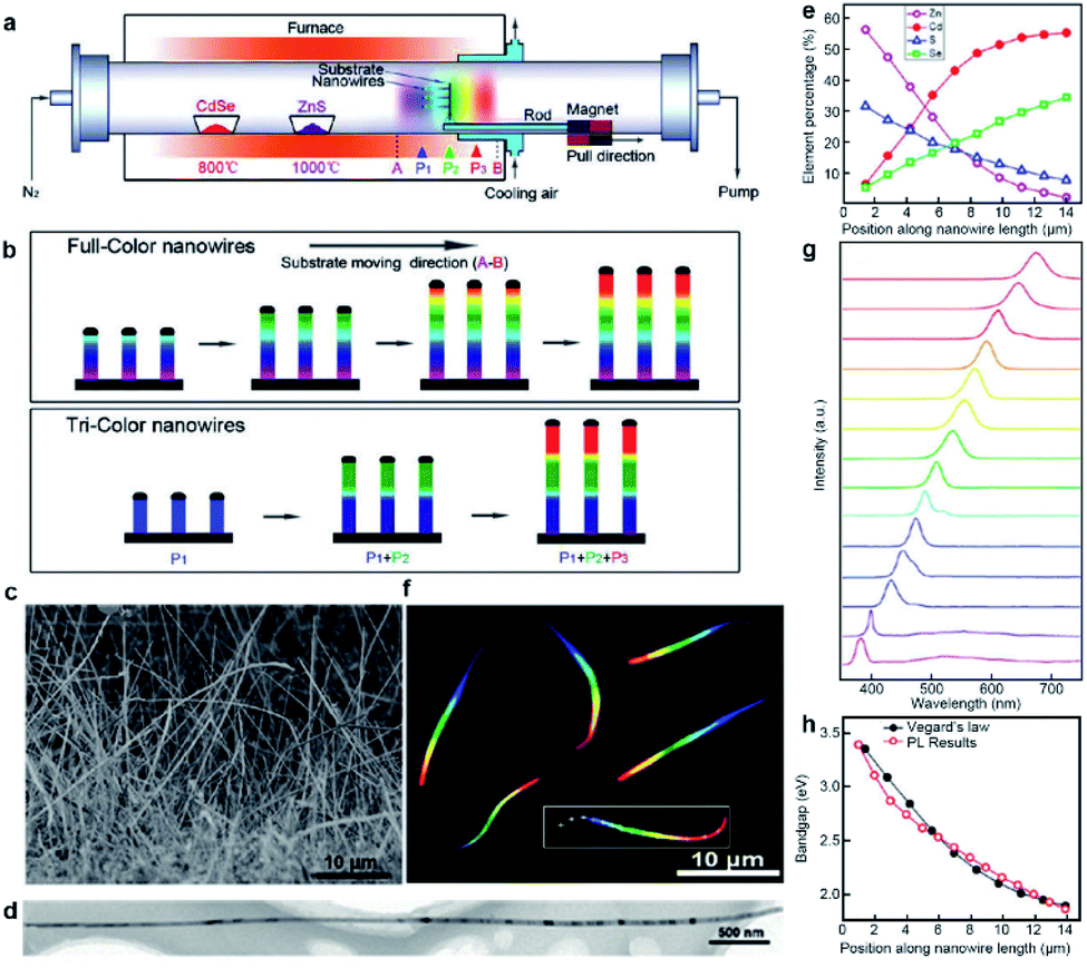 | ||
| Fig. 3 Composition-graded ZnyCd1−ySxSe1−x (0 ≤ x, y ≤ 1) nanowires. (a) Schematic diagram of substrate-moving thermal evaporation growth. (b) Schematic growth of full-color and tri-color nanowires. (c) SEM of as-grown nanowires. (d) TEM. (e) Position-dependent elemental molar fraction. (f) Real-color optical photograph of the dispersed nanowires under UV laser illumination. (g) Spatially resolved PL spectra acquired along a single nanowire (marked with a rectangle and crosses in panel (f)). (h) Position-dependent bandgaps calculated from the PL spectra (red circles) and the elemental compositions by the Vegard's law (black dots). Reproduced with permission.12 Copyright 2011, American Chemical Society. | ||
The composition-graded ZnCdSSe nanowires have a uniform diameter of ∼80 nm and a length of up to ∼30 μm (Fig. 3c and d). Spatially resolved EDS analysis indicates that any detected points along the nanowire length are composed of Zn, Cd, S, and Se elements. Fig. 3e reveals that Cd and Se increase gradually along the nanowire length while Zn and S are complementary to Cd and Se. Similar to the graded CdSxSe1−x nanowires, graded ZnyCd1−ySxSe1−x nanowires also have a high crystalline quality with the lattice spacing gradually varying along the growth axis. The most exciting result here is that these novel nanowires exhibit a rainbow-like emission colour under deep ultraviolet (UV) laser illumination, as shown beautifully in Fig. 3f. The red end corresponds to the Cd/Se-rich alloy, and the other grey end corresponds to the Zn/S-rich alloy with a bandgap or light emission extended into the UV region. Fig. 3g plots a series of spatially resolved PL spectra collected along the nanowire length. Each detected location has a single-band PL emission, with the peak wavelength gradually shifting from ∼380 nm to ∼700 nm, nearly covering the full visible spectrum. The local bandgap values can be derived from the PL spectra or calculated from the EDS quantitative results combined with Vegard's law for quaternary ZnyCd1−ySxSe1−x alloys. Fig. 3h shows that the bandgaps calculated from the PL spectra and EDS are well consistent with each other, confirming that all the emissions originate from the band-to-band transitions.
The above three examples of composition-graded nanowires not only reach the goal of single-nanostructure graded bandgap engineering but also provide a novel material choice for the emerging nano-optoelectronic applications. First of all, they are expected to serve as ultra-compact light sources packed with abundant wavelengths in view of their nanoscale footprint and finely tunable bandgaps.11,12 In particular, the emission color of ZnyCd1−ySxSe1−x nanowires covers the entire visible spectral range, and their nanoscale size is beyond the spatial resolution limit of the human naked eye. Consequently, they show high promise for use as monolithic white light sources. More details will be discussed in the Application section in this report.
It is worth mentioning that we made a great effort to grow composition-graded ZnyCd1−ySxSe1−x nanowires by the source-moving strategy before we moved to the substrate-moving strategy. The possible reason why we failed in growing composition-graded ZnyCd1−ySxSe1−x nanowires via the source-moving strategy is that the ZnS and CdSe compounds possess very different vapor pressures at the same temperature.52 Although in-depth research has to be done before reaching any reliable conclusions, we assume, based on our experimental experience, that the source-moving strategy may be only applicable to the combination of compounds that share a similar equilibrium vapor pressure at equal temperature, such as the CdS–CdSe system, while the substrate-moving strategy is preferable for combinations of compounds with considerable difference of equilibrium vapor pressures at equal temperature, e.g. the ZnS–CdS, ZnS–CdSe, and ZnSe–CdSe systems.
3. Axial hetero-nanowires
It is well known that the most revolutionary applications of semiconductors (i.e. diodes and transistors) rely on rational semiconductor heterojunctions. Therefore, considerable effort has been dedicated to the growth of hetero-nanowires ever since the birth of semiconductor nanostructures. Axial hetero-nanowires, where the composition or dopant experiences abrupt variations along the nanowire length, are particularly important for developing a list of nanowire functional devices, such as photodetectors, light-emitting diodes, field-effect transistors, thermoelectric components, and so on.6,17,70,72 A prerequisite for the optimal performance of these devices is the formation of high-quality sharp heterointerfaces.28 To date, most of the reported axial hetero-nanowires have been synthesized via other sophisticated approaches, rather than the facile thermal evaporation, as listed in the Introduction of this article.On the basis of the great success in the growth of composition-graded nanowires, we moved forward to the growth of axial hetero-nanowires by upgrading the source-moving strategy to the so-called multistep source-switching strategy with the same magnetic-pulling principle.47,50,73 The difference is that the pulling process is done as fast as possible to enable a fast source switching. Additional key to success of this source-switching growth is that a distinct time duration has to be introduced before switching to the next evaporation source in order to remove the residual of the previous source material as much as possible. On the basis of this source-switching strategy, two different axial hetero-nanowires have been fabricated so far. One is the CdS–CdSSe hetero-nanowires,46,50 the other is the GaSb–GaInSb hetero-nanowires.47
With CdS and CdSe powders serving as the evaporating sources, dual-segment CdS–CdSSe nanowires (Fig. 4a) and tri-segment CdS–CdSSe–CdS nanowires with long (Fig. 4b) and short (Fig. 4c) CdSSe segments are grown via the source-switching strategy by altering the growth parameters. The real-color photographs of these hetero-nanowires are shown in Fig. 4a–c, with green and red segments corresponding to the segments of CdS and CdSSe alloys, respectively. The CdSSe ternary alloy in these nanowires has a fixed S/Se ratio of ∼0.5, determined from EDS quantitative analyses, which is different from the gradually changed S/Se ratios in the graded nanowires. Fig. 4e shows a real-color emission photograph of a dual-segment hetero-nanowire, in which a sharp boundary between the green and red segment is clearly identified. Spatially resolved PL spectra (Fig. 4f) reveal that the green and red segments have a clean single-peak emission at 512 nm and 603 nm, respectively, with no obvious defect state-related emission, even around the hetero-interfaces. The spectrum from the junction (D3 in Fig. 4f) has two peaks with positions consistent with either the 512 nm green peak or 603 nm red peak, indicating that it originates from the two segments simultaneously, which is confirmed by 2D PL mapping. As shown in Fig. 4g, the 512 nm peak or 603 nm peak is only detected from the green and red segment, respectively, with a sharp boundary between them. The sharp boundary implies that the elemental composition is suddenly changed at the junctions, which is confirmed by the high-angle annular dark-field (HAADF) STEM image around the boundary (Fig. 4h). The transition length from CdS to CdSSe measured in the HAADF image is about 32 nm, which sets a new record of what can be reached by thermal evaporation growth, to the best of our knowledge. It is worth noting that the length of each segment in the tri-segment hetero-nanowires can be well controlled by adjusting the growth time. For example, the length of the middle CdSSe segment has been reduced from 40 μm (Fig. 4b) to 300 nm (Fig. 4c and i) by reducing the growth time for the CdSSe segment from 30 min to 2 min. This result suggests an improved controllability of thermal evaporation in terms of hetero-nanowire growth, although, unlike MOCVD and MBE growth, it remains a challenge to achieve sub-monolayer growth control and atomically sharp interfaces.
 | ||
| Fig. 4 Axial hetero-nanowires. Real-color optical photograph of (a) dispersed dual-segment CdS–CdSSe nanowires, dispersed tri-segment CdS–CdSSe nanowires with (b) long and (c) short red-emitting CdSSe segments in the middle, respectively. (d) SEM of as-grown GaSb–GaInSb nanowires. (e) Real-color optical photograph, (f) spatially resolved PL spectra, and (g) PL peak intensity mapping of a single dual-segment nanowire. (h) HAADF STEM image and line scanning profile of Se along the nanowire length. (i) EDS line profiles of Cd, Se and S across a single tri-segment hetero-nanowire with a short CdSSe segment in the middle. (j) 2D elemental mapping of GaSb–GaInSb nanowires. (a, e–h) Reproduced with permission.73 Copyright 2016, American Chemical Society. (b, c and i) Reproduced with permission.50 Copyright 2017, Elsevier B.V. (d and j) Reproduced with permission.47 Copyright 2014, American Chemical Society. | ||
On the basis of the same source-switching strategy, GaSb–GaInSb p–n nanowires are also synthesized with high-purity GaSb and InSb powders serving as the precursors. As-grown GaSb–GaInSb hetero-nanowires have a length of up to 20 μm and a diameter ranging from 80 nm to 200 nm (Fig. 4d). Unlike the straight CdS–CdSSe hetero-nanowires, GaSb–GaInSb hetero-nanowires have a regular kink structure with a bending angle of 120° (inset of Fig. 4d). The authors attribute this kink structure to the different growth temperatures for each segment. The mapping results (Fig. 4j) show that Ga and Sb are quite homogeneously distributed across the whole nanowire and In is almost completely confined in the top segment of the nanowire. Considering that intrinsic GaSb is a p-type semiconductor and GaInSb alloy is an n-type semiconductor,74,75 the elemental analyses results prove that these nanowires are GaSb–GaInSb p–n heterostructures.
4. Lateral hetero-nanobelts
The source-switching thermal evaporation growth has further been extended to grow two different multi-lane hetero-nanobelts under modified growth conditions. One is the CdS–CdS0.4Se0.6–CdS tri-lane hetero-nanobelt, in which a CdS0.4Se0.6 alloy nanobelt is sandwiched between two CdS nanobelts (Fig. 5a).45 Under laser illumination, the middle CdS0.4Se0.6 nanobelt and the two lateral CdS nanobelts exhibit red and green emission, respectively, thus each nanobelt looks like a colored tri-lane road, as shown in Fig. 5a. The other is exactly opposite, each nanobelt consists of a wide green CdS0.9Se0.1 nanobelt in the middle and two narrow red CdS0.5Se0.5 nanobelts on the two lateral sides (Fig. 5b).48 In addition, Kim et al. reported the growth of similar CdS/CdSe lateral heterostructure nanobelts by a two-step physical vapor transport method.76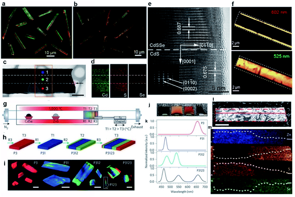 | ||
| Fig. 5 Lateral hetero-nanobelts. Real-color optical photograph of (a) CdS–CdS0.4Se0.6–CdS and (b) CdS0.5Se0.5–CdS0.9Se0.1–CdS0.5Se0.5 hetero-nanobelts. (c) TEM, (d) 2D elemental mapping, and (e) HRTEM image of CdS–CdS0.4Se0.6–CdS nanobelt. (f) PL peak intensity mapping of CdS0.5Se0.5–CdS0.9Se0.1–CdS0.5Se0.5 nanobelt. (g–m) Multi-lane ZnCdSSe hetero-nanobelts. (g) Schematic of the setup with a temperature gradient of 66 °C cm−1 in the region used for positioning the substrate. (h) Illustration of the growth procedure and the resulting samples. (i) PL images of individual structures after the corresponding growth sequences. Scale bars, 15 μm. (j) Digital photograph of as-grown samples under ambient lighting. (k) PL spectra of the samples shown in (i and j). (l) TEM image of a selected hetero-nanobelt for chemical elemental analysis. (m) EDS mapping inside the dashed rectangular area in (l). (a, c–e) Reproduced with permission.45 Copyright 2012, American Chemical Society. (b and f) Reproduced with permission.48 Copyright 2014, Wiley-VCH. (g–m) Reproduced with permission.15 Copyright 2015, Nature Publishing Group. | ||
Fig. 5c is the TEM morphology of the CdS–CdS0.4Se0.6–CdS nanobelt with a uniform width of ∼3 μm. EDS spectra acquired from three different positions along the width direction and 2D elemental mapping (Fig. 5d) reveal that Cd is quite uniformly distributed across the entire nanobelt, while S is located more concentrated on both lateral sides than in the central region, and Se almost completely occupies the central region of the nanobelt. The well-defined boundary in the elemental mapping images proves that these nanobelts are lateral heterostructures with CdS crystals forming both lateral lanes and CdS0.4Se0.6 ternary alloy in the middle lane. The HRTEM image reveals that no grain boundary exists at the CdS/CdS0.4Se0.6 hetero-interface (Fig. 5e), indicating the high quality of the heterojunction, which is reasonable since the lattice mismatch between CdS and CdS0.4Se0.6 is very small.45
The other CdS0.5Se0.5–CdS0.9Se0.1–CdS0.5Se0.5 lateral nanobelts share a similar tri-lane microstructure. The high quality of these nanobelts is also confirmed by their spatially resolved PL spectra and 2D PL intensity mapping (Fig. 5f). The peak wavelength of the emission bands at the lateral sides (602 nm) and the central region (525 nm) is consistent with the near-band-edge energy of the CdS0.5Se0.5 and CdS0.9Se0.1 alloys, respectively. The PL spectra collected at the interface exhibit two peaks, coming from the emission of both the central and the lateral regions simultaneously. Similar to the case of graded nanowires, all lateral nanobelts exhibit a clean band-edge emission with no obvious trap-level related emission observed across the entire nanobelt, including at the interface region, further confirming the high quality of these nanobelts and few defects even at the strained interface.
In 2015, Ning's group succeeded in the growth of multi-lane ZnCdSSe hetero-nanobelts via the multistep substrate-moving thermal evaporation assisted by magnetic force as well (Fig. 5g).15 The essence of this approach is to optimize the substrate temperature for the desired alloy composition by adjusting the substrate position along the axial temperature gradient in the tube reactor. Fig. 5g–k show schematically the whole growth procedure and the results from each step. The first step is the growth of Cd- and Se-rich red-emitting ZnCdSSe nanobelts at position R3 with temperature T3 ≈ 640 °C. These nanobelts are then moved to position R1 with temperature T1 ≈ 780 °C by driving the connected iron rod with an external magnet, where they are transformed to a Zn- and S-rich blue-emitting ZnCdSSe alloy with no appreciable change in morphology. The third step is the growth of the green-emitting lanes at position R2 with temperature T2 ≈ 740 °C by incorporating more Cd ions. Finally, the substrate is moved back to position R3 for the additional growth of the red-emitting lanes, resulting in the final multi-lane hetero-nanobelts capable of monolithic RGB light emission. The HRTEM images and the PL spectra (Fig. 5k) show that each lane of the nanobelt is a high-quality wurtzite monocrystal, with no visible defects or strain detected. Fig. 5l shows the morphology of a representative nanobelt used for chemical composition analyses, respectively. 2D mapping (Fig. 5m) results reveal that this nanobelt is composed of Zn, Cd, S and Se, and the concentration of these elements changes along the c axis. As one moves from the blue-emitting towards the red-emitting region, the concentrations of Cd and Se increase while those of Zn and S decrease. With this special nanobelt, a monolithic semiconductor laser capable of emitting over the full visible-color spectrum is demonstrated for the first time, which has a wide range of important applications, such as solid-state lighting, full-color displays, visible color communications and multi-color fluorescence sensing. Details will be discussed later in this report.
Another unexpected product we obtained by this magnetic-pulling thermal evaporation growth is the lateral composition-graded nanobelts.49 These special nanobelts are grown by the same source-moving thermal evaporation used for the growth of composition-graded nanowires but under different growth conditions. Elemental 2D mapping and line scanning results reveal that Cd is quite homogeneously distributed across the whole nanobelt, while S is gradually reduced and Se is gradually increased along the lateral direction. Under illumination of diffused laser light, each composition-graded nanobelt exhibits a gradually changed emission color from green to red along the ribbon width. The author attributes the formation of these composition-graded nanobelts to the polarization-induced asymmetric growth process.
5. Optoelectronic applications
The abovementioned examples of single-nanostructure bandgap engineering represent the latest advances in pursuing bandgap engineering at the nanoscale regime through the facile and cost-effective thermal evaporation growth. What is more important, a number of novel 1D semiconductor nanostructures are therefore obtained, providing a new material platform for both basic scientific research and nanodevice design. For example, composition-graded nanowires can directly serve as monolithic wavelength-tunable or multi-wavelength nanoscale light sources.11,12 Moreover, a growing list of functional components, including asymmetric light propagation,77 wavelength-converted waveguides,78 proof-of-concept wavelength splitters,78 broadband-response photodetectors,79–81 wavelength-tunable lasers,82,83 field-effect transistors,84 solar cells,84 and single-nanowire spectrometers,85 have been demonstrated based on these composition-graded nanowires. The axial hetero-nanowires show a high potential for performance improvement of nanowire photodetectors47,73 and threshold reduction of nanowire lasers.46 The multi-lane nanobelts have been employed as both gain medium and parallel resonant micro-cavity for dual-color,45,86 multi-color49,87,88 and even monolithic white-light lasers.15 In this section, we will discuss these impressive optoelectronic applications in detail.5.1 Monolithic white light sources
As stated above, the composition-graded nanowires integrate a list of position-dependent tunable bandgaps, making them promising wavelength-tunable or multi-wavelength nanoscale light sources. In particular, the PL from composition-graded ZnyCd1−ySxSe1−x nanowires covers the entire visible spectral range, therefore they have high potential to serve as trichromatic white-light sources since their nanoscale footprint is beyond the resolution of human naked eye. What is more interesting, the magnet-assisted substrate-moving growth allows one to control the length of each color segment by altering the growth time, consequently adjusting the relative emission intensity of each primary color, which eventually enables a rational control over the color temperature. As an example, the left panels in Fig. 6a–d show the real-color micrographs of the dispersed nanowires from four different samples with different RGB segments. Corresponding PL spectra (right panels in Fig. 6a–d) reveal that the relative intensity of the three primary colors is indeed tuned in accordance with the length variation of each color segment. Under low-magnification observation, white light spots with different color–temperature combinations are directly recorded with a color digital camera. As shown in Fig. 6e, samples T1, T2 and T3 exhibit light blue, light yellow, and orange PL emissions, respectively, while sample T4 possesses a nearly ideal white light emission. The calculated CIE (International Commission on Illumination) chromatic coordinates of samples T1–T3 are located at the edge of the white area in the CIE diagram, while that of sample T4 is located at the center of the white area (Fig. 6f), demonstrating the realization of nearly ideal white light emission from these graded nanowires by carefully adjusting the relative intensity of the three primary colors.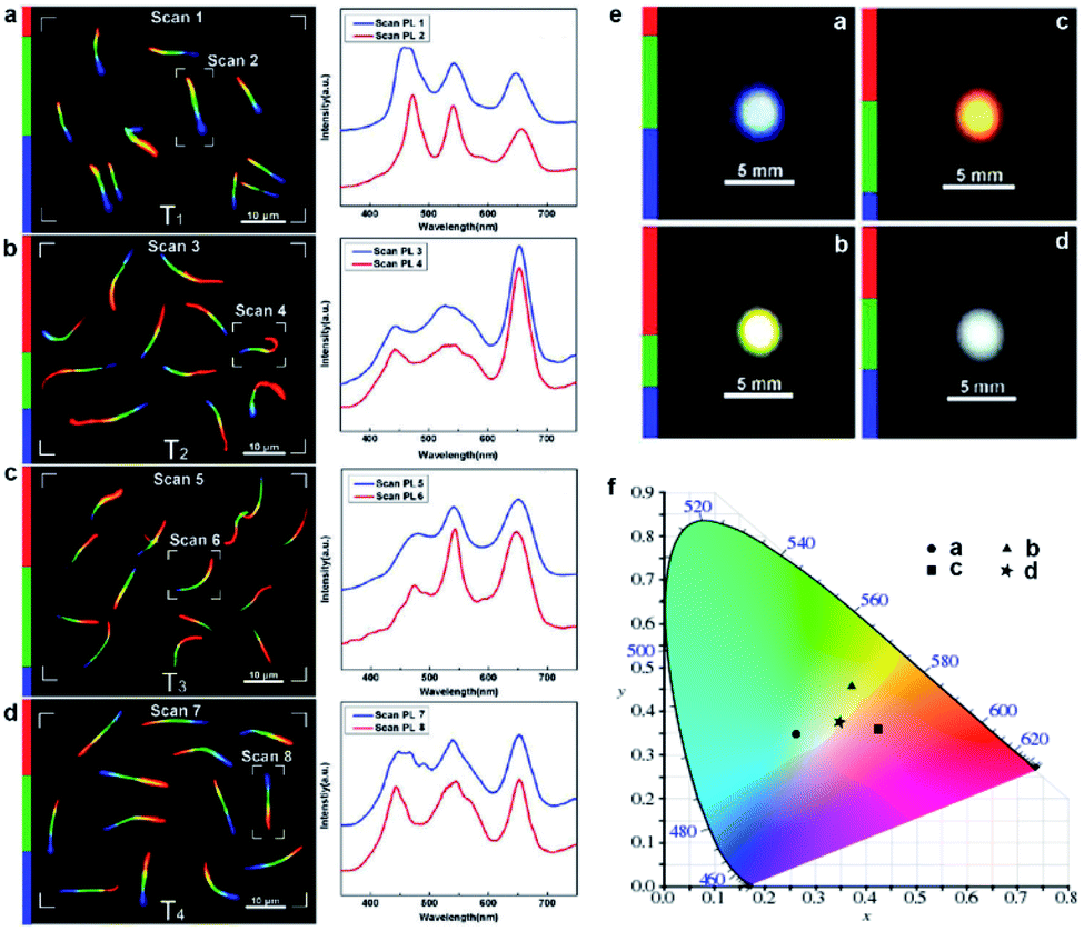 | ||
| Fig. 6 White-light emission from composition-graded nanowires. (a–d) Real-color micrographs (left) and corresponding PL spectra (right) of dispersed ZnyCd1−ySxSe1−x (0 ≤ x, y ≤ 1) nanowires from four tri-color samples (samples T1–T4), under 355 nm laser illumination. (e) Large area real-color photographs of the four samples under the illumination of a UV light beam. (f) CIE chromaticity diagram with the chromatic coordinates of the four tricolor samples calculated using the PL spectra shown on the right side of panels (a–d), respectively. Reproduced with permission.12 Copyright 2011, American Chemical Society. | ||
5.2 Photonic waveguides
Similar to optical fibers used for optical information communication in daily life, semiconductor nanowires have a two-dimensional confinement for visible light in their cross-section owing to their high refractive index contrast to their surroundings. In addition, semiconductor nanowires fabricated by thermal evaporation generally undergo a high-temperature process which offers them advantages of high single-crystalline quality, smooth surfaces, and nearly perfect geometry. Therefore, semiconductor nanowires have been utilized as excellent optical micro-cavities for light propagation and oscillation.89–92 In particular, the graded composition achieved in individual nanowires introduces not only a graded bandgap profile, but also a gradually changed dielectric constant along the nanowire length, which deserves special attention in terms of optical waveguiding. As a matter of fact, an unusual asymmetric light propagation has been observed in single composition-graded CdSSe nanowires from the perspective of guided light intensity, while from the perspective of guided light wavelength, a proof-of-concept wavelength splitter has been proposed based on the nanowire branch structure made of a composition-graded nanowire trunk and several composition-homogeneous nanowire branches.Fig. 7a and b show, respectively, the SEM view and real-color emission photograph of a composition-graded CdSSe nanowire. When the nanowire is independently excited at the nanowire ends with the same focused laser beam (input, Fig. 7c and d), the output light at the opposite ends has the same color but significantly different intensity. The PL spectra acquired at the output ends (Fig. 7e) further confirm that the light intensity contrast, C, at the two output ends is up to 0.95, demonstrating an excellent capability of asymmetric light propagation. Such a high intensity contrast is even close to the ideal contrast (C = 1) expected for a diode behavior, suggesting the potential for developing all-optical diodes.93–95 Theoretical studies suggest that the excellent asymmetric light propagation observed in these graded nanowires originates from the different propagation mechanisms along opposite directions. In the case of forward propagation toward the bandgap-increasing direction (Fig. 7c), the nanowire acts as a passive optical cavity for the input light (the PL coupled into the narrow-bandgap end) because the photon energy is smaller than the bandgap energy of any other positions along the nanowire. The input light will transmit through the nanowire cavity mainly by total internal reflection, exactly like how light transmits in a transparent optical fiber. Therefore, the propagation loss (both the optical intensity and the photon energy) is dominated by the band-tail absorption (induced by structural disorder) and the leakage caused by non-perfect geometry, which is very small for high quality nanowires. In the case of backward propagation toward the bandgap-decreasing direction (Fig. 7d), however, the nanowire acts as an active optical cavity for the input light (the PL coupled into the wide-bandgap end). The input light travels through the nanowire cavity by the incessantly repeated band-to-band re-absorption and re-emitting processes. The main contribution to propagation loss comes from the nonradiative loss involved in each band-to-band absorption and emitting process, which is orders of magnitude higher than the propagation loss for the forward passive waveguide.
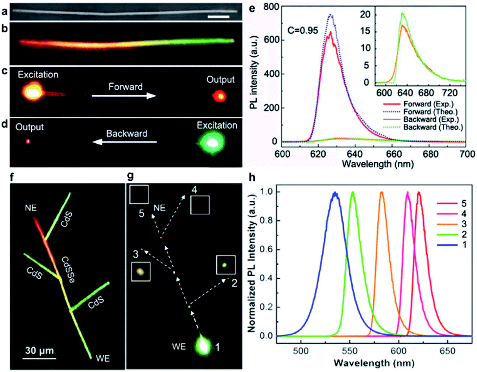 | ||
| Fig. 7 Optical waveguide. (a) SEM and (b) real-color emission photograph of a composition-graded CdSSe nanowire. Scale bar, 7 μm. (c and d) Real-color PL photographs with local excitation at one of its ends. (e) PL spectra at the output ends. The solid lines (red and orange) are the experimental results and dashed lines (blue and green) are the theoretical results, respectively. Inset shows the enlarged backward output PL spectra. (f and g) Real-color PL images of the nanowire branched structure under (f) diffused laser illumination and (g) focused excitation at the WE end of the trunk, respectively. Insets show the magnified (×4) views of the output signals at the output ends 2–5, respectively. (h) Detected spectra at the positions 1–5 indicated in panel (g), respectively. (a–e) Reproduced with permission.77 Copyright 2012, Nature Publishing Group. (f–h) Reproduced with permission.78 Copyright 2012, American Chemical Society. | ||
These nanowire-based asymmetric optical waveguides have some advantages, such as cost-effective setup, simple fabrication process, tunable working wavelengths, ultra-low operating power and nanoscale footprint, compared with previous all-optical diode designs based on planar chiral structures,96 liquid crystal heterojunctions,97 photonic crystals,98 absorbing multilayer structures,99 concentration-gradient fluorescent dyes,95 asymmetric optical resonators,100 and so on.93,94 However, it is worth noting that the guiding light inside the graded nanowires actually is the coupled PL emission induced by the input laser beam, instead of the original laser light. Therefore, this nanowire asymmetric optical waveguide can only serve as the so-called active optical waveguides at present, which is a fatal flaw for a lot of practical applications that usually require passive optical waveguides (where the guiding light is the original input light), such as the all-optical diodes required for the next generation of all-optical computing and processing. Nevertheless, the composition-graded nanowires still hold the possibility of realizing passive asymmetric optical waveguides by employing the gradient of dielectric constant along the nanowire length induced by the composition gradient.
The above discussion also indicates that the photon energy (wavelength) of the guided light in single composition-graded nanowires shifts continuously as it travels along the bandgap-decreasing direction. Therefore, single composition-graded nanowires can function as nanoscale wavelength converters. What is more interesting, this wavelength-converted waveguide behavior has been further used for development of a proof-of-concept nanoscale wavelength splitter. As shown in Fig. 7f, the proposed wavelength splitter consists of a nanowire-based branched structure, where the CdS branches are physically linked to the graded CdSSe backbone using the fiber-based micromanipulation incorporated in optical microscopy. When the green end of the graded CdSSe nanowire is locally excited with a focused laser beam (Fig. 7g), a small part of the PL emission from the excited end will couple into the nanowire body and further travel to the opposite end. The wavelength of the traveling light within the graded nanowire trunk will continuously increase as the propagation proceeds. Meanwhile, the wavelength-converted light inside the trunk can partially transmit into the branches through side-by-side coupling90 at each junction and further transmit passively along the CdS branches, in which additional wavelength shift is negligible since the CdS nanowire branches have a larger bandgap than that of any of the junctions in the graded nanowire trunk. In Fig. 7g, light spots with different colors and intensities are observed at each branch end (positions 2–4) as well as the opposite end of the graded nanowire (position 5). Corresponding intensity-normalized PL spectra in Fig. 7h confirm that light of different wavelengths has been extracted successfully from different CdS ends, therefore realizing the function of a wavelength splitter. The structure and involved fabrication steps of these nanowire-based wavelength converters and proof-of-concept wavelength splitters are much simpler than those of previously proposed schemes by other groups, such as photonic crystal,101 diffraction grating,102 or dielectric-loaded plasmonic waveguides.103 They will have great potential applications for optical information processing and communication in a compact photonic integrated system.18,101
5.3 Nanoscale lasers
1D semiconductor nanostructures with perfect geometry and smooth surface are ideal optical micro-cavities (i.e. Fabry–Pérot or whispering-gallery mode) in view of the high dielectric constant of semiconductors. Meanwhile, they provide the necessary gain media required for light to reach lasing thresholds. Therefore, they have been suggested as promising candidates for developing nanoscale lasers.10 Since the first demonstration of ZnO nanowire lasers in 2001 by Yang et al.,89 a large number of 1D nanostructure-based lasers have been investigated. Most of them are optically pumped lasers made of individual composition-homogeneous 1D nanostructures, such as the well investigated II–VI, III–V family and their alloys, and the brand new perovskite nanostructures.104 In principle, the lasing properties (i.e. lasing modes, quality factors, thresholds) of 1D semiconductor nanostructures are determined by their sizes, bandgaps, and geometry. Therefore, the single-nanostructure bandgap engineering in these composition-engineered 1D nanostructures is expected to play a key role in their lasing behavior. For example, the composition-graded CdSSe nanowires are capable of defining tunable lasing wavelengths over a wide range.82,83,88 In contrast, the dual composition-graded CdSSe nanowires are considered as more perfect optical resonant cavities, reducing the nanowire lasing threshold because they can effectively suppress the band tail induced self-absorption.46 The multi-lane lateral hetero-nanobelts provide monolithically integrated cavities in a parallel configuration, which allows light with different wavelengths to lase simultaneously, therefore realizing dual-color,45 tri-color,49 and even monolithic RGB white-light15 lasers from individual 1D semiconductor nanostructures.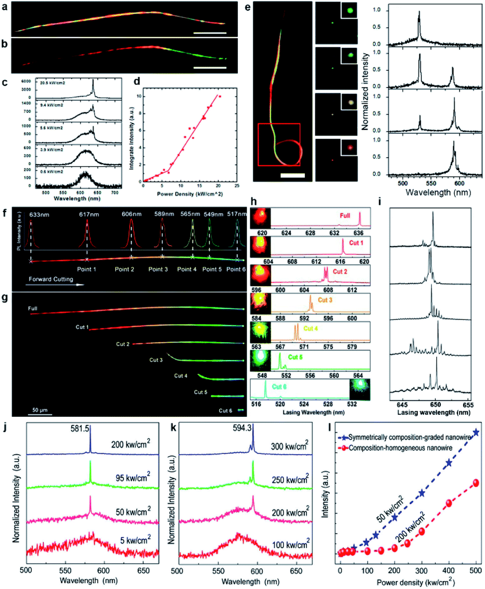 | ||
| Fig. 8 Composition-graded nanowire lasers. (a) Dark-field optical photograph and (b) real-color image of a composition-graded CdSSe nanowire. Scale bars are 30 μm. (c) PL spectra under a single excitation pulse with increasing peak power density. (d) Integrated intensity of 637 nm lasing peak versus excitation power density. (e) Color control of a looped wire dual-color laser. Left is the dark-field image of the looped nanowire. Scale bar, 10 μm. Middle panels are the real-color images under different pumpings for the two cavities. The images are taken from the red box. Right is the normalized lasing spectra acquired from the middle panels. (f) Real-color image of a composition-graded CdSSe nanowire with six cut points determined by the localized PL spectra. (g) Real-color images and (h) lasing spectra of the nanowire after being cut at point 1 to point 6 sequentially. The colorful spots shown in each spectrum correspond to the real-color image of the end emission of each nanowire at pump density above the threshold. (i) Lasing spectra obtained by cutting the nanowire along the bandgap-decreasing direction step-by-step. (j and k) Pumping power-dependent PL spectra of symmetrically composition-graded nanowires and composition-homogeneous CdSSe alloy nanowires, respectively. (l) Integrated intensity of the lasing peaks at 581.5 nm and 594.3 nm versus excitation power density. (a–e) Reproduced with permission.83 Copyright 2013, American Chemical Society. (f–i) Reproduced with permission.82 Copyright 2014, American Chemical Society. (j–l) Reproduced with permission.46 Copyright 2013, American Chemical Society. | ||
Nevertheless, it is interesting to investigate whether single graded nanowires could lase at different colors simultaneously since they naturally integrate abundant tunable bandgaps in one ultra-small cavity. Such a goal first came true by looping the wide-bandgap end of a graded nanowire to form a relatively isolated nano-ring cavity for the green emission,83 as illustrated in Fig. 8e. The nano-ring cavity in this configuration provides a strong feedback for the green emission from the wide-bandgap end,105,106 hence significantly reducing the re-absorption of the green emission by the straight nanowire tail with smaller bandgaps. In the meantime, the orange emission from the narrow-bandgap end can still propagate in the entire nanowire. As a result, the green emission can oscillate in the nano-ring cavity with sufficient gain and low loss to reach the lasing level, while the orange emission can still oscillate to lase in the cavity defined by the two end-facets of the nanowire. More interestingly, this configuration enables a color-tunable laser by pumping the straight and looped segments separately with modulated laser intensities. As shown in the dark-field images (Fig. 8e), the output color at the junction was tuned from green (B1) to yellow-green (B2) to yellow (B3) to orange (B4) by simply adjusting the relative intensities of the two pump beams. The corresponding lasing spectra (right side in Fig. 8e) confirm that the intensity of the green and orange lasing peaks is well modulated by adjusting the pumping intensities, which eventually leads to the tunable lasing color.
Another way to extract the integrated different lasing wavelengths from these composition-graded nanowires was reported by Yang et al. in 2014.82 As shown in Fig. 8f–h, tuned laser colors from red to green with tunable wavelengths over a wide range of 119 nm are achieved by cutting a single composition-graded CdSSe alloy nanowire along the bandgap-increasing direction step-by-step. In contrast, if the nanowire is step-by-step cut along the bandgap-decreasing direction, its sharp lasing modes are always located in the broad PL peak from the CdSe-rich end (Fig. 8i). The free spectral range of these lasing modes shows a linear relationship with L−1, where L is the nanowire length after each cutting, indicating the well-defined Fabry–Pérot cavity properties originating from the reflection at the two end facets of the nanowire.89,91 Therefore, further cutting the nanowire into even shorter lengths may end up with single-mode lasing, which is another active research topic in the field of nanowire lasers.
As stated above, the red laser from the CdSe-end of the composition-graded CdSSe nanowire also indicates that a passive optical cavity is more favorable than an active optical cavity in terms of reducing the lasing threshold of nanowires. Such a deduction is further proven by the investigation of the lasing behavior of symmetrically composition-graded CdSSe alloy nanowires46 as well as tri-segment axial hetero-nanowires.50 As shown in Fig. 8j–l, the symmetrically composition-graded CdSSe nanowires start to lase at a threshold of ∼50 kW cm−2, which is several times lower than the threshold of the composition-homogeneous CdS nanowire lasers (∼200 kW cm−2). As a result of the symmetrically increased bandgaps from the middle to the two ends, the nanowire is optically transparent for the light emitted from the middle segment that has the narrowest bandgap (red emission). In this case, the propagation loss of the red emission is expected to be much smaller than that in homogeneous nanowires because both the band-to-band absorption and the self-absorption induced by the band tails92,107 are eliminated during oscillation between the two nanowire end facets. Owing to the same reason, similar results are obtained when the middle narrow bandgap segment of the tri-segment axial hetero-nanowires is pumped to lase.50
Room-temperature dual-color lasing was first observed from individual CdS–CdSSe–CdSe tri-lane hetero-nanobelts,45 as can be seen in the pumping power-dependent lasing spectra (Fig. 9a). The 607.9 nm red and 517.9 nm green lasing peaks originate from the middle CdSSe lane and the two lateral CdS lanes, respectively. The lasing threshold of the red emission (∼80 kW cm−2) is a lot lower than that of the green emission (∼200 kW cm−2). Although the threshold of a semiconductor laser is determined by a series of factors, such as the optical gain of materials and the amount of gain materials,91 here the inevitable re-absorption of the green emission by the middle CdSSe lane is the main reason that caused the difference in lasing thresholds. More interestingly, the lasing peak at the longer side of the wavelength can be tuned by adjusting the S/Se ratio in the middle CdSSe lanes, as shown in Fig. 9b. Fan et al. reported similar results in 2013 as well.86
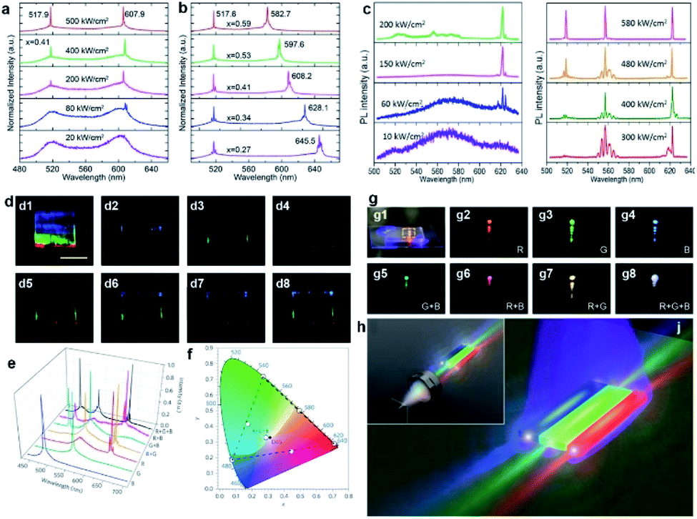 | ||
| Fig. 9 Monolithic multi-color lasers based on single lateral hetero-nanobelts. (a) Power-dependent PL spectra of a CdS–CdSSe tri-lane hetero-nanobelt. (b) Lasing spectra from CdS–CdSSe tri-lane hetero-nanobelts with different S/Se ratios (x) in the middle lanes. (c) Power-dependent PL spectra of a CdS–CdSSe lateral graded nanobelt. (d) Real-color images of a single ZnCdSSe multi-lane nanobelt, under low pumping (d1) and above-threshold pumping (d2–d8). (e) Corresponding PL spectra acquired from panels d2 to d8. (f) Chromaticity of the lasing peaks extracted from the spectra in (e). (g1) Photograph of the mixed emission colour. (g2–g8) Photographs of the enlarged dashed-box region in (g1) when the different combinations of segments are pumped as indicated by the labels inside each figure, creating the mixed far-field emission colours red, green, blue, yellow, cyan, magenta and white. The top dots in each photograph are the direct images of laser emission, while the tails under these dots are the reflections from the substrate. (h) Schematic diagram for achieving a monolithic white laser from an individual multi-lane hetero-nanobelt. (a and b) Reproduced with permission.45 Copyright 2012, American Chemical Society. (c) Reproduced with permission.49 Copyright 2016, Springer. (d–h) Reproduced with permission.15 Copyright 2015, Nature Publishing Group. | ||
On the basis of lateral composition-graded CdSSe nanobelts, multi-color lasers with three groups of lasing modes at 519 nm (green), 557 nm (orange), and 623 nm (red), respectively, have been reported at room temperature (Fig. 9c).49 In-depth studies revealed that the red lasing mode originates from the passive Fabry–Pérot cavity89,91 resonance between the two end facets of the longer length direction. The orange and green lasing modes, however, in accordance with the passive and active Fabry–Pérot modes, oscillate between the two lateral facets along the width direction, respectively.
The most exciting achievement of monolithic multi-color lasers is the first realization of a monolithic white-light laser from individual ZnCdSSe multi-lane hetero-nanobelts.15 Three power adjustable beams are focused into long, narrow, parallel stripes to pump one of the three segments each. Fig. 9d shows the optical properties of such a multi-lane hetero-nanobelt under different pumping conditions. By pumping one, two and all three lanes up to their lasing thresholds, the author demonstrated independent lasing of each RGB color, simultaneous two-color lasing of any two of the three primary colors, and finally simultaneous RGB mixed white color lasing. Fig. 9e presents the lasing spectra for all the seven cases, while Fig. 9f shows the calculated chromaticity for these lasing spectra on a CIE1931 color diagram. The chromaticity of the carefully balanced white lasing is very close to that of the white point CIE standard white illuminant D6546. The corresponding far-field photograph in Fig. 9g confirms the following: (1) independent red, green and blue lasing can be achieved by pumping each color lane individually (g2–g4); (2) yellow, cyan and magenta mixed lasing emissions are produced by pumping two of the segments (g5–g7); (3) simultaneous RGB lasing emission from a single multi-segment hetero-nanobelt can be mixed together to render white-like color (g8). This color mixing demonstration provides an experimental proof-of-concept for the use of multi-color lasing structures for illumination and display applications (Fig. 9h).
5.4 Photodetectors
Another intensively investigated application of 1D semiconductor nanostructures is the photodetector (or optical sensor) considering the fact that the electrical conductivity of semiconductors usually increases in accordance with the incident light intensity. In principle, the photoconductivity involves several successive or simultaneous physical processes:108 (1) absorption of incident light; (2) exciton generation by the incident light with photon energy larger than the nanostructure bandgap, which determines the spectral response of the photoconductor; (3) carrier (electrons and holes) separation due to an applied electrical field, which induces the photocurrent; (4) exciton recombination at the surface and in the bulk of the nanostructures, which leads to photocurrent degradation; (5) carrier trapping and releasing by defect centers, which determine the rise time and decay time when the incident radiation is introduced and withdrawn, respectively. They are all closely related to the bandgap diagram of the nanostructures, therefore the abovementioned single-nanostructure bandgap engineering induced by the engineered composition is expected to bring additional impact on their photoconductivity characteristics.The first example is a monolithic wavelength-selective (multispectral) photodetector by taking advantage of the graded bandgaps along the nanowire length axis.79 This multispectral photodetector consists of individual graded CdSSe nanowires with 4 parallel electrodes deposited (Fig. 10a). By connecting adjacent electrodes, three photodetector cells (PD1, PD2, PD3) are integrated in a series configuration, each covering a different bandgap band. As a result, each detector is expected to have its unique response to a different spectral range. Fig. 10b plots the photocurrent as a function of incident wavelength. The response cutoff wavelengths extrapolated for PD1–PD3 at forward bias and PD3 at reverse bias are 540, 570, 600, and 630 nm, respectively. The rectification ratio, defined as the ratio of forward current to backward current, is closely related to the excitation wavelength. As plotted in Fig. 10c, the rectification ratio of each detector exhibits a single peak feature, with peak wavelengths at 550, 570, and 600 nm, respectively, which correspond to the response cutoff wavelengths in Fig. 10b. Although a similar tunable wavelength response range is implementable based on CdSSe nanowire arrays with a composition gradient along a single substrate,109 here the tunable ranges are monolithically integrated into a single nanowire. Besides, the integrated number of photodetector units can be increased by simply adding more parallel electrodes onto the graded nanowires, hence increasing the selectivity of the photodetector. Such a monolithic multispectral system greatly increases the sensitivity of photodetectors beyond what single spectral photodetectors are capable of.
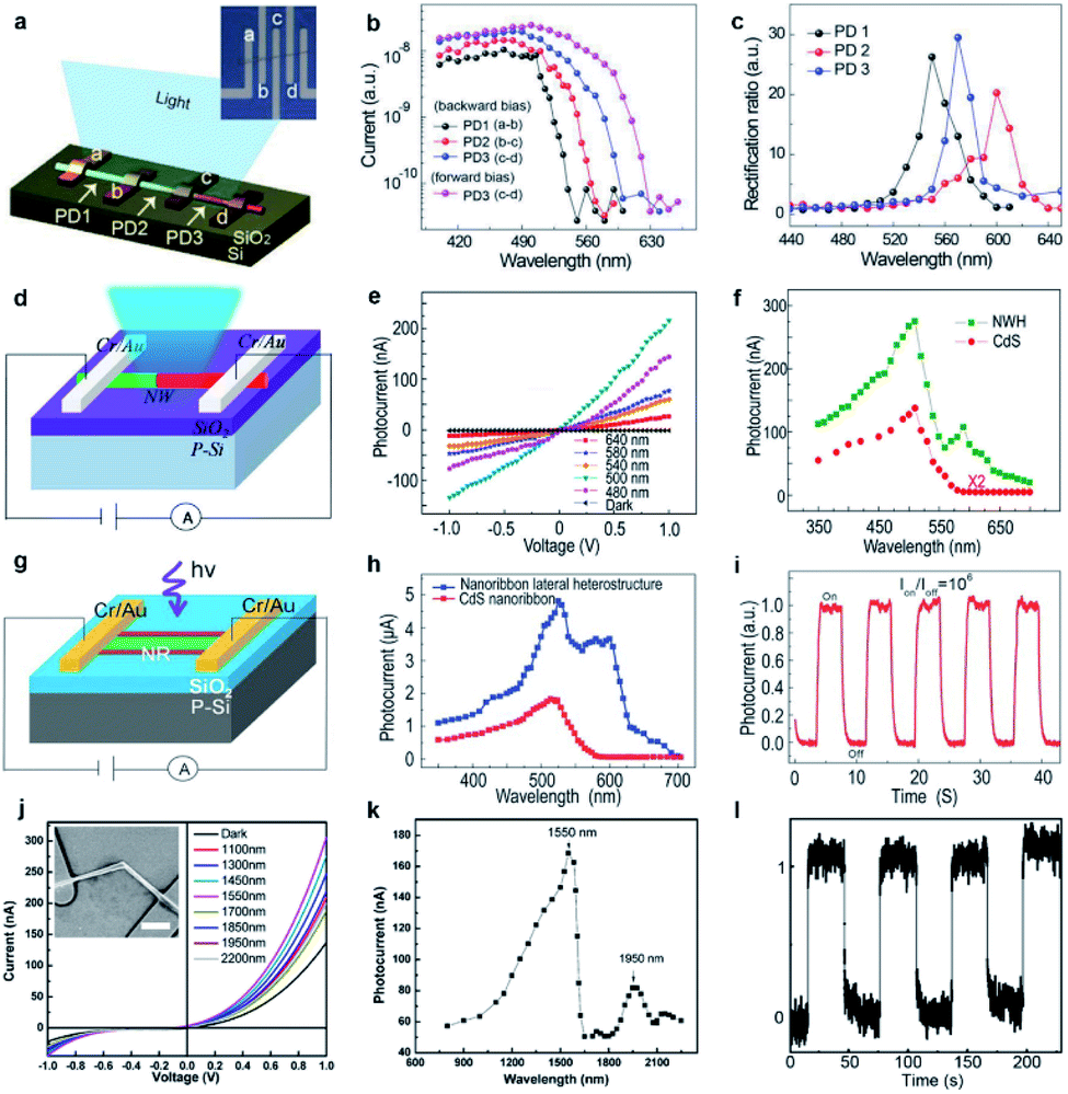 | ||
| Fig. 10 Photodetectors based on composition-engineered 1D semiconductor nanostructures. (a–c) Wavelength selective photodetector made of a single composition-graded CdSSe nanowire: (a) schematic drawing; (b) wavelength-dependent photocurrents; (c) wavelength-dependent rectification ratios. (d–f) Photodetector made of a single CdS–CdSSe axial hetero-nanowire: (d) schematic drawing; (e) I–V curves under dark conditions and illumination of different laser wavelengths with the same intensity; (f) excitation wavelength-dependent photocurrents of the detectors made of an axial hetero-nanowire (green) and a homogeneous CdS nanowire (red), respectively. (g–i) Photodetectors made of a single tri-lane hetero-nanobelt: (g) schematic drawing; (h) excitation wavelength-dependent photocurrents of the detectors made of single tri-lane hetero-nanobelts (blue) and homogeneous CdS nanobelt (red), respectively; (i) photocurrent under illumination of an intensity-modulated laser. (j–l) Photodetector made of a single GaSb–GaInSb p–n hetero-nanowire: (j) I–V curves under dark conditions and illumination of different infrared laser wavelengths with the same intensity; (k) excitation wavelength-dependent photocurrent; (l) photocurrent under illumination of an intensity-modulated 1550 nm laser. (a–c) Reproduced with permission.79 Copyright 2018, Wiley-VCH. (d–f) Reproduced with permission.73 Copyright 2016, American Chemical Society. (g–i) Reproduced with permission.48 Copyright 2014, Wiley-VCH. (j–l) Reproduced with permission.47 Copyright 2014, American Chemical Society. | ||
The change of the conductivity induced by incident irradiation depends upon not only the bandgap absorption of the semiconductor, but also the number of free carriers produced per absorbed photon and the mobility of these carriers.108,110 The abruptly changed bandgap in 1D axial hetero-nanostructures is expected to enhance the separation of photogenerated carriers. Fig. 10d depicts schematically the construction of a photodetector made of a single CdS–CdS0.49Se0.51 axial hetero-nanowire. Under the illumination of laser beams of different wavelengths with the same intensity, the conductance of the CdS–CdS0.49Se0.51 axial hetero-nanowire is indeed increased significantly, on the one hand. On the other hand, the increment depends on the wavelength being used (Fig. 10e). Fig. 10f further reveals that two response bands with peak positions at 512 nm and 603 nm, respectively, are recognized for this axial hetero-nanowire detector, which is much broader than the single response band at 512 nm observed for the homogeneous CdS nanowire detector. The two response bands are expected results since the CdS and CdS0.49Se0.51 segments in the same nanowire possess a stronger photon absorption ability for these two bands owing to their band-to-band absorption. Besides, the photocurrent of axial hetero-nanowire detectors is always higher than that of CdS nanowire detectors, indicating improved photoconductivity in the investigated spectral band (from 350 nm to 700 nm). The author ascribed this improved photoconductivity to the broadened absorption bands in the hetero-nanowire and the re-absorption of the CdS emission by the CdS0.49Se0.51 segment with a narrower bandgap. In addition, the rise time and fall time of the CdS–CdS0.49Se0.51 axial hetero-nanowire detector are reduced to 68 μs and 137 μs, respectively, which are at least 1 order of magnitude shorter than those of the CdS nanowire detector (1.6 ms and 3.7 ms, respectively).
On the basis of CdS0.5Se0.5–CdS0.9Se0.1–CdS0.5Se0.5 lateral hetero-nanobelts, a high performance photodetector is also demonstrated (Fig. 10g).48 Similar to the axial hetero-nanowire detector, this detector exhibits increased photoconductivity compared to the homogeneous CdS nanobelt detector in a broad spectral range from 350 nm to 700 nm (Fig. 10h). The rise time and fall time of this hetero-nanobelt detector are 30 ms and 90 ms (Fig. 10i), respectively, 1 order of magnitude shorter than the case of the CdS nanobelt detector (280 ms and 550 ms, respectively). Although the hetero-nanobelt detector has a longer rise and fall time than the hetero-nanowire detector, the responsivity (1.16 × 10³ A W−1) and gain (104), are 1 and 2 orders of magnitude higher than those of the hetero-nanowire detector (1.18 × 10² and 3.1 × 10²), respectively. As suggested by the Rose model,111–114 there is a tradeoff between the gain and the response speed of semiconductor detectors since both gain and response speed are determined by the lifetime of the photo-generated carriers.
Until now, most photodetectors made of 1D semiconductor nanostructures exhibit a notable response to a certain spectral band in the visible range. Progress in developing infrared photodetectors from 1D nanostructures, however, is limited. On the basis of the GaSb–GaInSb p–n hetero-nanowires, we reported a near-infrared nanowire photodetector that works at room temperature.47 As shown in Fig. 10j, all the I–V curves acquired for different incident infrared light wavelengths but same intensity show a well-defined rectification characteristic owing to the formation of a p–n junction in the GaSb–GaInSb hetero-nanowire. Compared with the electrical conductance under dark conditions, the electrical conductance of the nanowire increases dramatically under light illumination. Fig. 10k further shows that the photodetector exhibits a dual-band spectral response as well. The peak wavelengths of these two bands are located at 1550 nm and 1950 nm, in consistence with the band-to-band charge generation processes of the GaSb and Ga0.9In0.1Sb segments, respectively. Fig. 10l indicates that this near-IR photodetector exhibits features of a high external quantum efficiency of 104, a high responsivity of 103 A W−1 and a response time as short as 2 ms. It is worth pointing out that the strongest response band at 1550 nm is exactly the wavelength that is most widely used in optical communication systems. Therefore, these photodetectors may be compatible with the existing optical communication systems. Besides, the nanoscale footprint of these devices offers them great potential for future on-chip integrated nanosystems.
5.5 Field-effect transistors and solar cells
Similar to the case of 1D nanostructure photodetectors, most of the early reported field-effect transistors (FETs) and solar cells are built up from individual composition-homogeneous nanostructures that are randomly selected from the growth substrate.115–119 The impact of engineered composition in single 1D nanostructures has rarely been investigated.70,74 On the basis of composition-graded CdS1−xSex alloy nanowires, Li et al. carried out the initial study on their FETs and solar cells. The FET is made of single composition-graded CdS1−xSex alloy nanowire with a back-gate configuration. The acquired output characteristics reveal that this FET has a pronounced gate-dependent Ids–Vds effect and n-type conductivity. From the linear region of the transfer characteristics, the threshold gate voltage, Vth, and the transconductance, gm, are determined to be −8.2 V and 18.6 nS, respectively. Consequently, the calculated electron mobility is 1.5 cm2 V−1 s −1 and the concentration is 2.1 × 1017 cm−3. The on–off current ratio of such FETs is up to 107. In addition, a CdSxSe1−x nanowire-network Schottky solar cell was fabricated and characterized under air-mass (AM) 1.5 G illumination. This device exhibits a current density (Jsc) of 13.1 mA cm−2, an open-circuit voltage (Voc) of 0.21 V, a fill factor (FF) of 28%, and an energy conversion efficiency (η) of 0.77%. These results are comparable to or even higher than the values measured for pure CdS117 and CdSe118 nanowire/nanobelt cells. The monochromatic incident photon-to-electron conversion efficiency (IPCE) spectrum shows that the solar cell maintains a high photo-electron response in the whole visible range. However, such a nanowire-network Schottky solar cell has been far from perfect so far. The energy conversion efficiency is still quite low and the dispersed nanowires are too disordered to reach the upper limit of the theoretical performance. Possible strategies for further performance improvement will be discussed in the Conclusion section.5.6 Single-nanowire spectrometer
The latest exciting optoelectronic application of composition-graded nanowires is the single-nanowire spectrometer, reported last year by Yang et al. In their report, a composition-graded CdSxSe1−x nanowire covered from 1.74 eV to 2.42 eV in bandgaps (Fig. 11a) was firstly transferred from the growth substrate onto a Si/SiO2 substrate and served as the active element of the spectrometer. An array of In/Au parallel electrodes (top, Fig. 11b) with identical spacing was then deposited on the graded nanowire to form a good electrical contact. After incorporating the graded nanowire into a packaged chip (bottom, Fig. 11b), a single-nanowire spectrometer was successfully constructed for the first time. With such a simple configuration, each segment of the graded nanowire between two neighboring electrodes functioned as an ultra-compact photodetector. Under illumination of adequate light, each cell showed a good photo-response characteristic with typical response and recovery time of ∼1.5 ms and 3.5 ms, respectively (Fig. 11c). In principle, photocurrent or photo-response only emerges when the incident photon energy is larger than the bandgap energy of the semiconductor materials. As a result of the graded bandgaps between adjacent photodetector cells, the response cutoff wavelengths and normalized spectral responses Ri(λ) of the photodetector cell shifted continuously along the nanowire (Fig. 11d) under the same radiation. Therefore, the incident light spectrum can be reconstructed by taking into account the pre-calibrated photon-response and signal discrepancy of each detector unit (Fig. 11e). The minimum reconstructed FWHM achieved by the nanowire spectrometer with 38 detector units is 7 nm (Fig. 11f), which is comparable with the FWHM measured using a conventional spectrometer (Thorlabs CCS100, 0.5 nm wavelength accuracy). At present, the spectrometer can well resolve two peaks around 570 nm separated by 15 nm. Despite a reduction in footprint of about two to three orders of magnitude, such a resolution is comparable to that of other visible-range spectral reconstruction micro-spectrometers, and commercially available centimeter-scale systems. Furthermore, the authors demonstrated an in situ, micrometer-scale spectral imaging, which has long been a great challenge across fields such as cytobiology and biomedicine, using their nanowire spectrometer on the basis of a shift register strategy (Fig. 11g–k). As an example, a red onion cell membrane, featuring naturally colored cells surrounded by transparent cells, was mounted onto the sample holder and positioned over the nanowire spectrometer with a gap of several micrometers (Fig. 11g and h). Under the illumination of white light, the nanowire spectrometer scanned across the x–y plane with fixed mapping steps (Fig. 11i). The scanning results provided simultaneously the intensity maps at fixed wavelength (Fig. 11j) and the reconstructed absorption spectra for different points on the onion cell membrane (Fig. 11k), suggesting that this spectrometer has high potential to obtain spectral images at the cellular level.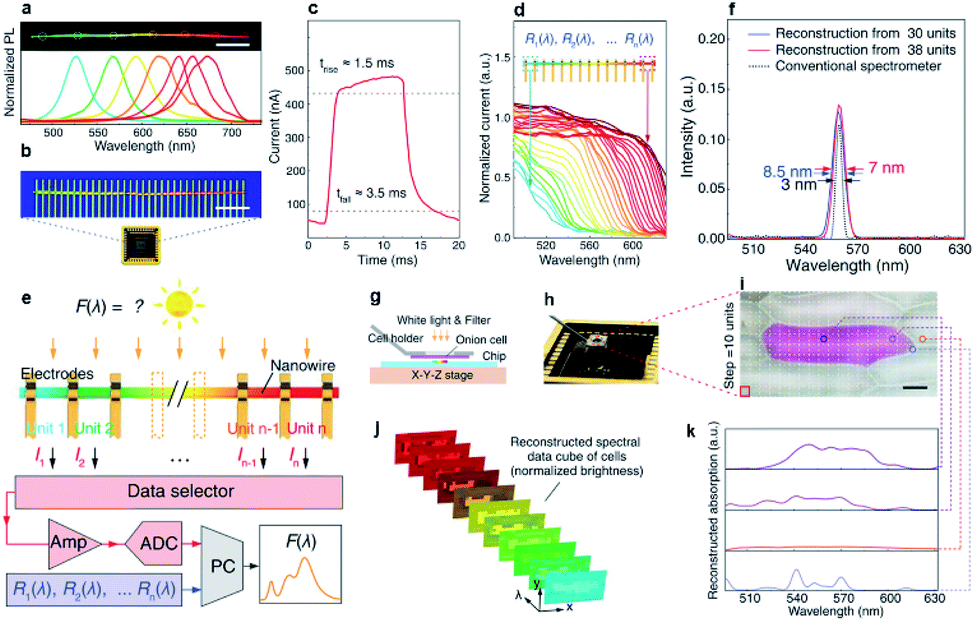 | ||
| Fig. 11 Spectrometer based on single composition-graded CdSxSe1−x nanowires. (a) PL real-color digital image of a selected composition-graded CdSxSe1−x nanowire and corresponding PL spectra collected from the circle-marked regions (spot size ∼ 5 μm). Scale bar, 20 μm. (b) Fluorescent micrograph (top) of a nanowire spectrometer, incorporated into a packaged chip (bottom). Scale bar, 10 μm. (c) Time response measured between two neighboring electrodes at the red (CdSe) end of the nanowire under intensity-modulated incident light (490 nm, 0.3 mW cm−2) at a bias of 0.5 V. Dotted lines indicate 10 and 90% of peak value, as used for calculating the rise (1.5 ms) and fall time (3.5 ms). (d) Normalized spectral responses Ri(λ) of each constituent unit in the nanowire spectrometer, with cutoff wavelengths shifting continuously along the nanowire length. (e) Operational scheme of the nanowire spectrometer. (f) Measurement and reconstruction of a single spectral peak at 560 nm using a 30- and 38-unit device, relative to the same signal measured by a conventional spectrometer (Thorlabs CCS100, 0.5 nm wavelength accuracy). Arrows indicate the FWHM. (g–k) Spectral imaging at the micrometer scale: (g) operational scheme of cell mapping; (h) photograph of the cell-mapping apparatus; (i) micrograph of a naturally pigmented red onion cell surrounded by transparent cells. Scale bar: 50 mm; (j) absorption spectral images of the onion cell at selected wavelengths. Pixel intensity range of these images is normalized; (k) reconstructed absorption spectra from different parts of the red onion cell membrane. Reproduced with permission.85 Copyright 2019, American Association for the Advancement of Science. | ||
6. Concluding remarks and future perspectives
In summary, the past ten years have witnessed great progress in single-nanostructure composition/bandgap engineering by upgrading conventional thermal evaporation systems with a home-made magnetic-pulling module. Several different magnetic-pulling strategies have been proposed for bottom-up growth of diverse composition-engineered 1D semiconductor nanostructures, consequently offering various single-nanostructure bandgap engineering desired for future nano-optoelectronics. The first is the in situ “source-moving” strategy, which enabled the growth of CdSSe ternary alloy nanowires with a linear composition gradient or symmetrical dual composition gradients along the nanowire length, as well as CdSSe ternary alloy nanobelts with a composition gradient along the nanobelt width. The second is the in situ “substrate-moving” strategy, which allowed the growth of composition-graded ZnCdSSe quaternary alloy nanowires and multi-lane ZnCdSSe hetero-nanobelts. The third is the multi-step “source-switching” strategy, which let us succeed in the growth of axial hetero-nanowires and tri-lane CdSSe hetero-nanobelts. On the basis of these composition-engineered 1D semiconductor nanostructures, a number of laboratory nanodevices have been proposed for optoelectronic applications, including ultra-small monolithic wavelength-tunable light sources, monolithic white-light sources, asymmetric light propagation, wavelength converters and splitters, color-tunable nano-lasers, low-threshold nanowire lasers, monolithic dual-color, multi-color and even white-color nanostructure lasers, monolithic wavelength selective and broadband-response photodetectors in the visible and IR spectral range, transistors, solar cells as well as the very recent exciting single-nanowire spectrometer.Despite the great progress in the growth and promising optoelectronic applications of composition-engineered 1D semiconductor nanostructures based on this magnetic-pulling thermal evaporation strategy, many opportunities and challenges remain for the future. First and foremost, site-controlled horizontal alignment is necessary in order to further realize the substantial potential of these novel 1D nanostructures. For example, composition-graded nanowires on a single chip have recently been suggested as a fascinating material platform for developing the so-called spectrum-splitting photovoltaic system120,121—which enables optimized absorption of different solar spectral components by a combination of the matched bandgaps available in these graded nanowires and the assistance of dispersive optical elements (such as prisms).122 In this regard, site-controlled horizontally aligned composition-graded nanowire arrays (Fig. 12a) are highly anticipated in order to construct such spectrum-splitting photovoltaic systems for further improvement of the energy conversion efficiency of nanowire solar cells, as schematically shown in Fig. 12b. The great news is that considerable progress in site-controlled growth of horizontally oriented semiconductor nanowires through the facile thermal evaporation has been made by suitably choosing the substrate and growth conditions over the past two decades. To date, a growing list of semiconductor nanowires have been successfully grown on either flat surfaces through the guiding effect of the substrate lattices123–129 or faceted surfaces with pre-formed aligned nano-features (i.e. nanogrooves, nanosteps) by the so-called “graphoepitaxy”,9,32–40 where nanowires are guided by the aligned orientation of the nano-features. Very recently, the generality of guided growth has been further applied to the growth of self-aligned core–shell nanowires with controlled growth sites and shells, allowing a scale-up fabrication of nanowire photodetectors with both high-gain and ultrafast response.114 With these ideas in mind, there will be a great chance for success in the site-controlled growth of composition-engineered 1D semiconductor nanostructure arrays by combining the magnetic-pulling thermal evaporation strategy with the in-plane guided growth mechanism. Second, controlled growth of p–n hetero-nanowire horizontal arrays for light emitting diodes (Fig. 12c) and n–p–n hetero-nanowire horizontal arrays for transistors remains a challenge, which deserves even more research enthusiasm. Third, it is worthwhile to make efforts to extend the general synthesis strategy to the growth of narrow-bandgap III–V semiconductors for the purpose of photodetector applications in the near and deep IR spectral range. Last but not least, the principle of this magnetic-pulling thermal evaporation is not limited to the growth of composition-engineered 1D semiconductor nanostructures. As a matter of fact, this strategy has been successfully applied to the growth of composition-modulated 2D layered nanomaterials,130 such as composition-graded atomic layer MoS2(1−x)Se2x (ref. 131) and WS2(1−x)Se2x (ref. 132) nanobelts, as well as WS2–WSe2 and MoS2–MoSe2 atomic layered heterostructures,133 and so on.
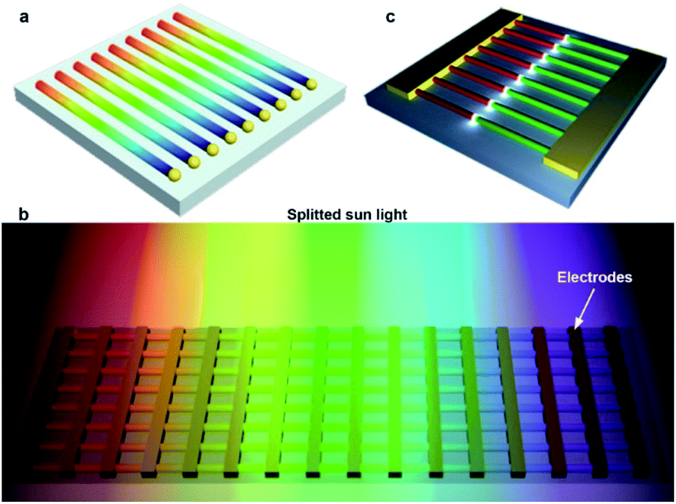 | ||
| Fig. 12 Challenges and opportunities of single-nanostructure bandgap engineering. (a) Self-oriented growth of horizontal arrays of composition-graded nanowires. (b) Conceptual scheme of a spectrum-splitting photovoltaic system based on composition-graded nanowire arrays. (c) Light-emitting diodes made of in-plane arrays of p–n hetero-nanowires. | ||
From the perspective of technology, some optimization work is anticipated in order to further improve the capability of composition control of thermal evaporation growth. For example, it remains a substantial challenge to grow nanowire superlattices based on thermal evaporation because thin nanowires are usually too delicate to survive multiple sequential growth steps, which however are necessary for the formation of nanowire superlattices. In principle, block-by-block growth of nanowire superlattices requires an effective minimization of undesired homogeneous nucleation of new crystal seeds to ensure exclusive heterogeneous epitaxial growth at the two ends of the existing nanowires. Such a goal has been achieved in the robust growth of superlattices from 2D atomic crystals by introducing a reverse gas flow during the temperature-swing stage in the sequential vapor deposition growth process.134 In this regard, incorporating the reverse flow strategy into the magnetic-pulling thermal evaporation system to enable block-by-block growth of nanowire superlattices is another research direction worthwhile to make an effort in the near future. Last but not least, further improvement of alignment quality (i.e. nanowire density, length uniformity, industrial-scale)135,136 is essential toward the next-step large-scale fabrication of optoelectronic devices and systems based on bottom-up 1D semiconductor nanostructures.
Conflicts of interest
There are no conflicts to declare.Acknowledgements
The authors acknowledge the financial support by the 2019QN01C290, the Outstanding Young Scholar at South China Normal University, Science and Technology Program of Guangzhou (No. 2019050001), Program for Chang Jiang Scholars and Innovative Research Teams in Universities (No. IRT_17R40), Guangdong Provincial Key Laboratory of Optical Information Materials and Technology under Grant (No. 2017B030301007), MOE International Laboratory for Optical Information Technologies and the 111 Project. National Natural Science Foundation of China (No. 61504116).Notes and references
- A. Pan, R. Liu, M. Sun and C. Ning, J. Am. Chem. Soc., 2009, 131, 9502 CrossRef CAS PubMed.
- A. Pan, H. Yang, R. Liu, R. Yu, B. Zou and Z. Wang, J. Am. Chem. Soc., 2005, 127, 15692 CrossRef CAS PubMed.
- Y. Liu, J. Zapien, Y. Shan, C. Geng, C. Lee and S. Lee, Adv. Mater., 2005, 17, 1372 CrossRef CAS.
- C.-Z. Ning, L. Dou and P. Yang, Nat. Rev. Mater., 2017, 2, 1 Search PubMed.
- X. Zhuang, C. Ning and A. Pan, Adv. Mater., 2012, 24, 13 CrossRef CAS PubMed.
- J. Arbiol, M. de la Mata, M. Eickhoff and A. Morral, Mater. Today, 2013, 16, 213 CrossRef CAS.
- Y. Xia, P. Yang, Y. Sun, Y. Wu, B. Mayers, B. Gates, Y. Yin, F. Kim and Y. Yan, Adv. Mater., 2003, 15, 353 CrossRef CAS.
- H. Yan, H. Choe, S. Nam, Y. Hu, S. Das, J. Klemic, J. Ellenbogen and C. Lieber, Nature, 2011, 470, 240 CrossRef CAS PubMed.
- M. Schvartzmana, D. Tsiviona, D. Mahalub, O. Raslinb and E. Joselevich, Proc. Natl. Acad. Sci. U. S. A., 2013, 110, 15195 CrossRef PubMed.
- S. Eaton, A. Fu, A. Wong, C. Ning and P. Yang, Nat. Rev. Mater., 2016, 1, 1 Search PubMed.
- F. Gu, Z. Yang, H. Yu, J. Xu, P. Wang, L. Tong and A. Pan, J. Am. Chem. Soc., 2011, 133, 2037 CrossRef CAS PubMed.
- Z. Yang, J. Xu, P. Wang, X. Zhuang, A. Pan and L. Tong, Nano Lett., 2011, 11, 5085 CrossRef CAS PubMed.
- Y. Ra, R. Navamathavan, H. Yoo and C. Lee, Nano Lett., 2014, 14, 1537 CrossRef CAS PubMed.
- Y. Qu and X. Duan, J. Mater. Chem., 2012, 22, 16171 RSC.
- F. Fan, S. Turkdogan, Z. Liu, D. Shelhammer and C. Z. Ning, Nat. Nanotechnol., 2015, 10, 796 CrossRef CAS PubMed.
- Y. Wu, R. Fan and P. Yang, Nano Lett., 2002, 2, 83 CrossRef CAS.
- M. Gudiksen, L. Lauhon, J. Wang, D. Smith and C. Lieber, Nature, 2002, 415, 617 CrossRef CAS PubMed.
- F. Qian, Y. Li, S. Gradečak, H.-G. Park, Y. Dong, Y. Ding, Z. L. Wang and C. M. Lieber, Nat. Mater., 2008, 7, 701 CrossRef CAS PubMed.
- M. Hocevar, G. Immink, M. Verheijen, N. Akopian, V. Zwiller, L. Kouwenhoven and E. Bakkers, Nat. Commun., 2012, 3, 1 Search PubMed.
- W. Guo, M. Zhang, A. Banerjee and P. Bhattacharya, Nano Lett., 2010, 10, 3355 CrossRef CAS PubMed.
- T. Rieger, M. Luysberg, T. Schäpers, D. Grützmacher and M. I. Lepsa, Nano Lett., 2012, 12, 5559 CrossRef CAS PubMed.
- L. Li, D. Pan, Y. Xue, X. Wang, M. Lin, D. Su, Q. Zhang, X. Yu, H. So, D. Wei, B. Sun, P. Tan, A. Pan and J. Zhao, Nano Lett., 2017, 17, 622 CrossRef CAS PubMed.
- H. Kim, H. Rho, E. Lee and J. Song, J. Phys. D: Appl. Phys., 2016, 49, 175105 CrossRef.
- M. Laskar, S. Carnevale, A. Sarwar, P. Phillips, M. Mills and R. Myers, J. Electron. Mater., 2013, 42, 863 CrossRef CAS.
- F. Furtmayr, J. Teubert, P. Becker, S. Conesa-Boj, J. R. Morante, A. Chernikov, S. Schäfer, S. Chatterjee, J. Arbiol and M. Eickhoff, Phys. Rev. B: Condens. Matter Mater. Phys., 2011, 84, 205303 CrossRef.
- H. Geaney, E. Mullane, Q. Ramasse and K. Ryan, Nano Lett., 2013, 13, 1675 CrossRef CAS PubMed.
- G. Flynn, Q. Ramasse and K. Ryan, Nano Lett., 2016, 16, 374 CrossRef CAS PubMed.
- C.-Y. Wen, M. C. Reuter, J. Bruley, J. Tersoff, S. Kodambaka, E. A. Stach and F. M. Ross, Science, 2009, 326, 1247 CrossRef CAS PubMed.
- R. Nötzel, Natl. Sci. Rev., 2017, 4, 184 CrossRef.
- R. Wagner and W. Ellis, Appl. Phys. Lett., 1964, 4, 89 CrossRef CAS.
- Z. Pan, Z. Dai and Z. Wang, Science, 2001, 291, 1947 CrossRef CAS PubMed.
- L. Goren-Ruck, D. Tsivion, M. Schvartzman, R. Popovitz-Biro and E. Joselevich, ACS Nano, 2014, 8, 2838 CrossRef CAS PubMed.
- E. Shalev, E. Oksenberg, K. Rechav, R. Popovitz-Biro and E. Joselevich, ACS Nano, 2017, 11, 213 CrossRef CAS PubMed.
- E. Oksenberg, R. Popovitz-Biro, K. Rechav and E. Joselevich, Adv. Mater., 2015, 27, 3999 CrossRef CAS PubMed.
- G. Reut, E. Oksenberg, R. Popovitz-Biro, K. Rechav and E. Joselevich, J. Phys. Chem. C, 2016, 120, 17087 CrossRef CAS PubMed.
- D. Tsivion and E. Joselevich, J. Phys. Chem. C, 2014, 118, 19158 CrossRef CAS.
- J. Xu, E. Oksenberg, R. Popovitz-Biro, K. Rechav and E. Joselevich, J. Am. Chem. Soc., 2017, 139, 15958 CrossRef CAS PubMed.
- D. Tsivion and E. Joselevich, Nano Lett., 2013, 13, 5491 CrossRef CAS PubMed.
- D. Tsivion, M. Schvartzman, R. Popovitz-Biro, P. v. Huth and E. Joselevich, Science, 2011, 333, 1003 CrossRef CAS PubMed.
- D. Tsivion, M. Schvartzman, R. Popovitz-Biro and E. Joselevich, ACS Nano, 2012, 6, 6433 CrossRef CAS PubMed.
- S. Xu, Y. Ding, Y. Wei, H. Fang, Y. Shen, A. Sood, D. Polla and Z. Wang, J. Am. Chem. Soc., 2009, 131, 6670 CrossRef CAS PubMed.
- E. Oksenberg, E. Sanders, R. Popovitz-Biro, L. Houben and E. Joselevich, Nano Lett., 2018, 18, 424 CrossRef CAS PubMed.
- M. Shoaib, X. Zhang, X. Wang, H. Zhou, T. Xu, X. Wang, X. Hu, H. Liu, X. Fan, W. Zheng, T. Yang, S. Yang, Q. Zhang, X. Zhu, L. Sun and A. Pan, J. Am. Chem. Soc., 2017, 139, 15592 CrossRef CAS PubMed.
- W. Deng, X. Zhang, J. Wang, Q. Shang, C. Gong, X. Zhang, Q. Zhang and J. Jie, Org. Electron., 2014, 15, 1317 CrossRef CAS.
- J. Xu, L. Ma, P. Guo, X. Zhuang, X. Zhu, W. Hu, X. Duan and A. Pan, J. Am. Chem. Soc., 2012, 134, 12394 CrossRef CAS PubMed.
- P. Guo, X. Zhuang, J. Xu, Q. Zhang, W. Hu, X. Zhu, X. Wang, Q. Wan, P. He, H. Zhou and A. Pan, Nano Lett., 2013, 13, 1251 CrossRef CAS PubMed.
- L. Ma, W. Hu, Q. Zhang, P. Ren, X. Zhuang, H. Zhou, J. Xu, H. Li, Z. Shan, X. Wang, L. Liao, H. Q. Xu and A. Pan, Nano Lett., 2014, 14, 694 CrossRef CAS PubMed.
- P. Guo, W. Hu, Q. Zhang, X. Zhuang, X. Zhu, H. Zhou, Z. Shan, J. Xu and A. Pan, Adv. Mater., 2014, 26, 2844 CrossRef CAS PubMed.
- X. Zhuang, P. Guo, Q. Zhang, H. Liu, D. Li, W. Hu, X. Zhu, H. Zhou and A. Pan, Nano Res., 2016, 9, 933 CrossRef CAS.
- Q. Zhang, H. Liu, P. Guo, D. Li, P. Fan, W. Zheng, X. Zhu, Y. Jiang, H. Zhou, W. Hu, X. Zhuang, H. Liu, X. Duan and A. Pan, Nano Energy, 2017, 32, 28 CrossRef CAS.
- P. Reimers and W. Ruppel, Phys. Status Solidi B, 1968, 29, K13 Search PubMed.
- P. Reimers, Phys. Status Solidi B, 1969, 35, 707 CrossRef CAS.
- L. Van Ruyven and I. Dev, J. Appl. Phys., 1966, 37, 3324 CrossRef.
- Indradev, L. V. Ruyven and F. Williams, J. Appl. Phys., 1968, 39, 3344 CrossRef CAS.
- A. Pan, W. Zhou, E. S. P. Leong, R. Liu, A. H. Chin, B. Zou and C. Z. Ning, Nano Lett., 2009, 9, 784 CrossRef CAS PubMed.
- T. Kuykendall, P. Ulrich, S. Aloni and P. Yang, Nat. Mater., 2007, 6, 951 CrossRef CAS PubMed.
- A. L. Pan, R. B. Liu, M. H. Sun and C. Z. Ning, ACS Nano, 2010, 4, 671 CrossRef CAS PubMed.
- K. Seo, S. Lee, H. Yoon, J. In, K. S. K. Varadwaj, Y. Jo, M. H. Jung, J. Kim and B. Kim, ACS Nano, 2009, 3, 1145 CrossRef CAS PubMed.
- H. Li, C. Cheng, X. Li, J. Liu, C. Guan, Y. Tay and H. Fan, J. Phys. Chem. C, 2012, 116, 3802 CrossRef CAS.
- Y. Wang, J. Xu, P. Ren, X. Zhuang, H. Zhou, Q. Zhang, X. Zhu and A. Pan, Mater. Lett., 2013, 105, 90 CrossRef CAS.
- K. Davami, J. Pohl, M. Shaygan, N. Kheirabi, H. Faryabi, G. Cuniberti, J. S. Lee and M. Meyyappan, Nanoscale, 2013, 5, 932 RSC.
- Y. Wang, J. Xu, P. Ren, Q. Zhang, X. Zhuang, X. Zhu, Q. Wan, H. Zhou, W. Hu and A. Pan, Phys. Chem. Chem. Phys., 2013, 15, 2912 RSC.
- R. Pinyun, H. Wei, Z. Qinglin, Z. Xiaoli, Z. Xiujuan, M. Liang, F. Xiaopeng, Z. Hong, L. Lei, D. Xiangfeng and P. Anlian, Adv. Mater., 2014, 26, 7444 CrossRef PubMed.
- P. L. Nichols, Z. Liu, L. Yin, S. Turkdogan, F. Fan and C. Z. Ning, Nano Lett., 2015, 15, 909 CrossRef CAS PubMed.
- A. Dong, F. Wang, T. Daulton and W. Buhro, Nano Lett., 2007, 7, 1308 CrossRef CAS PubMed.
- J.-E. Yang, W.-H. Park, C.-J. Kim, Z. H. Kim and M.-H. Jo, Appl. Phys. Lett., 2008, 92, 26311 Search PubMed.
- Y. He, J. Fan and Y. Zhao, Cryst. Growth Des., 2010, 10, 4954 CrossRef CAS.
- C. Kim, K. Kang, Y. Woo, K. Ryu, H. Moon, J. Kim, D. Zang and M. Jo, Adv. Mater., 2007, 19, 3637 CrossRef CAS.
- S. Dayeh, R. Dickerson and S. Picraux, Appl. Phys. Lett., 2011, 99, 113105 CrossRef.
- S. Le, P. Jannaty, X. Luo, A. Zaslavsky, D. Perea, S. Dayeh and S. Picraux, Nano Lett., 2012, 12, 5850 CrossRef CAS PubMed.
- L. Vegard, Z. Phys., 1921, 5, 17 CrossRef CAS.
- C. Yang, Z. Zhong and C. M. Lieber, Science, 2005, 310, 1304 CrossRef CAS PubMed.
- P. Guo, J. Xu, K. Gong, X. Shen, Y. Lu, Y. Qiu, J. Xu, Z. Zou, C. Wang, H. Yan, Y. Luo, A. Pan, H. Zhang, J. Ho and K. Yu, ACS Nano, 2016, 10, 8474 CrossRef CAS PubMed.
- B. Borg, K. Dick, B. Ganjipour, M. Pistol, L. Wernersson and C. Thelander, Nano Lett., 2010, 10, 4080 CrossRef CAS PubMed.
- P. Dutta, H. Bhat and V. Kumar, J. Appl. Phys., 1997, 81, 5821 CrossRef CAS.
- Y. Kim, J. Jung, H. Yoon, M. Song, S. H. Bae, Y. Kim, Z. Chen, J. Zou, H. Joyce, Q. Gao, H. Tan and C. Jagadish, Nanotechnology, 2010, 21, 145602 CrossRef PubMed.
- J. Xu, X. Zhuang, P. Guo, X. Zhu, Z. Yang, L. Tong, X. Duan, W. Huang, W. Hu, Q. Zhang and A. Pan, Sci. Rep., 2012, 2, 820 CrossRef PubMed.
- J. Xu, X. Zhuang, P. Guo, Q. Zhang, W. Huang, Q. Wan, W. Hu, X. Wang, X. Zhu, C. Fan, Z. Yang, L. Tong, X. Duan and A. Pan, Nano Lett., 2012, 12, 5003 CrossRef CAS PubMed.
- X. Hu, H. Liu, X. Wang, X. Zhang, Z. Shan, W. Zheng, H. Li, X. Wang, X. Zhu, Y. Jiang, Q. Zhang, X. Zhuang and A. Pan, Adv. Opt. Mater., 2018, 6, 1800293 CrossRef.
- F. Gu, H. Yu, W. Fang and L. Tong, Appl. Phys. Lett., 2011, 99, 181111 CrossRef.
- H. Liu, J. Lu, Z. Yang, J. Teng, L. Ke, X. Zhang, L. Tong and C. H. Sow, Sci. Rep., 2016, 6, 27387 CrossRef CAS PubMed.
- Z. Yang, D. Wang, C. Meng, Z. Wu, Y. Wang, Y. Ma, L. Dai, X. Liu, T. Hasan, X. Liu and Q. Yang, Nano Lett., 2014, 14, 3153 CrossRef CAS PubMed.
- Z. Liu, L. Yin, H. Ning, Z. Yang, L. Tong and C. Ning, Nano Lett., 2013, 13, 4945 CrossRef CAS PubMed.
- L. Li, H. Lu, Z. Yang, L. Tong, Y. Bando and D. Golberg, Adv. Mater., 2013, 25, 1109 CrossRef CAS PubMed.
- Z. Yang, T. Albrow-Owen, H. Cui, J. Alexander-Webber, F. Gu, X. Wang, T.-C. Wu, M. Zhuge, C. Williams, P. Wang, A. Zayats, W. Cai, L. Dai, S. Hofmann, M. Overend, L. Tong, Q. Yang, Z. Sun and T. Hasan, Science, 2019, 365, 1017 CrossRef CAS PubMed.
- F. Fan, Z. Liu, L. Yin, P. Nichols, H. Ning, S. Turkdogan and C. Ning, Semicond. Sci. Technol., 2013, 28, 065005 CrossRef.
- S. Turkdogan, F. Fan and C.-Z. Ning, Adv. Funct. Mater., 2016, 26, 8521 CrossRef CAS.
- Y. Lu, F. Gu, C. Meng, H. Yu, Y. Ma and W. Fang, Opt. Express, 2013, 21, 22314 CrossRef PubMed.
- M. H. Huang, S. Mao, H. Feick, H. Yan, Y. Wu, H. Kind, E. Weber, R. Russo and P. Yang, Science, 2001, 292, 1897 CrossRef CAS PubMed.
- M. Law, D. J. Sirbuly, J. C. Johnson, J. Goldberger, R. J. Saykally and P. Yang, Science, 2004, 305, 1269 CrossRef CAS PubMed.
- J. Johnson, H. Yan, P. Yang and R. Saykally, J. Phys. Chem. B, 2003, 107, 8816 CrossRef CAS.
- A. Pan, X. Wang, P. He, Q. Zhang, Q. Wan, M. Zacharias, X. Zhu and B. Zou, Nano Lett., 2007, 7, 2970 CrossRef CAS PubMed.
- L. Fan, J. Wang, L. T. Varghese, H. Shen, B. Niu, Y. Xuan, A. M. Weiner and M. Qi, Science, 2012, 335, 447 CrossRef CAS PubMed.
- L. Bi, J. Hu, P. Jiang, D. H. Kim, G. F. Dionne, L. C. Kimerling and C. Ross, Nat. Photonics, 2011, 5, 758 CrossRef CAS.
- S. Mujumdar and H. Ramachandran, Opt. Lett., 2001, 26, 929 CrossRef CAS PubMed.
- V. Fedotov, A. Schwanecke, N. Zheludev, V. Khardikov and S. Prosvirnin, Nano Lett., 2007, 7, 1996 CrossRef CAS.
- J. Hwang, M. H. Song, B. Park, S. Nishimura, T. Toyooka, J. Wu, Y. Takanishi, K. Ishikawa and H. Takezoe, Nat. Mater., 2005, 4, 383 CrossRef CAS PubMed.
- Z. Wang, Y. Chong, J. D. Joannopoulos and M. Soljačić, Nature, 2009, 461, 772 CrossRef CAS PubMed.
- R. Philip, M. Anija, C. S. Yelleswarapu and D. Rao, Appl. Phys. Lett., 2007, 91, 141118 CrossRef.
- J. Fujita, M. Levy, R. Osgood Jr, L. Wilkens and H. Dötsch, Appl. Phys. Lett., 2000, 76, 2158 CrossRef CAS.
- H.-G. Park, C. J. Barrelet, Y. Wu, B. Tian, F. Qian and C. M. Lieber, Nat. Photonics, 2008, 2, 622 CrossRef CAS.
- H. Taylor, Opt. Commun., 1973, 8, 421 CrossRef.
- Z. Chen, T. Holmgaard, S. I. Bozhevolnyi, A. V. Krasavin, A. V. Zayats, L. Markey and A. Dereux, Opt. Lett., 2009, 34, 310 CrossRef CAS PubMed.
- H. Zhu, Y. Fu, F. Meng, X. Wu, Z. Gong, Q. Ding, M. Gustafsson, M. Trinh, S. Jin and X. Zhu, Nat. Mater., 2015, 14, 636 CrossRef CAS PubMed.
- P. J. Pauzauskie, D. J. Sirbuly and P. Yang, Phys. Rev. Lett., 2006, 96, 143903 CrossRef PubMed.
- R. Ma, X. Wei, L. Dai, S. Liu, T. Chen, S. Yue, Z. Li, Q. Chen and G. Qin, Nano Lett., 2009, 9, 2697 CrossRef CAS PubMed.
- F. Urbach, Phys. Rev., 1953, 92, 1324 CrossRef CAS.
- J. Jie, W. Zhang, I. Bello, C.-S. Lee and S.-T. Lee, Nano Today, 2010, 5, 313 CrossRef CAS.
- T. Takahashi, P. Nichols, K. Takei, A. C. Ford, A. Jamshidi, M. CWu, C. Z. Ning and A. Javey, Nanotechnology, 2012, 23, 045201 CrossRef PubMed.
- X. Dai, M. Tchernycheva and C. Soci, in Semiconductors and Semimetals, ed. A. F. i. M. Shadi, A. Dayeh and J. Chennupati, Elsevier, 2016, vol. 94, pp. 75–107 Search PubMed.
- A. Rose, Proc. IRE, 1955, 43, 1850 CAS.
- R. Bube, Proc. IRE, 1955, 43, 1836 CAS.
- A. Rose, Phys. Rev., 1955, 97, 322 CrossRef.
- J. Xu, K. Rechav, R. Popovitz-Biro, I. Nevo, Y. Feldman and E. Joselevich, Adv. Mater., 2018, 30, 1800413 CrossRef PubMed.
- P. Wu, Y. Ye, C. Liu, R. Ma, T. Sun and L. Dai, J. Mater. Chem., 2009, 19, 7296 RSC.
- Y. Ye, L. Dai, X. Wen, P. Wu, R. Pen and G. Qin, ACS Appl. Mater. Interfaces, 2010, 2, 2724 CrossRef CAS.
- Y. Ye, Y. Dai, L. Dai, Z. Shi, N. Liu, F. Wang, L. Fu, R. Peng, X. Wen, Z. Chen, Z. Liu and G. Qin, ACS Appl. Mater. Interfaces, 2010, 2, 3406 CrossRef CAS PubMed.
- L. Zhang, Y. Jia, S. Wang, Z. Li, C. Ji, J. Wei, H. Zhu, K. Wang, D. Wu, E. Shi, Y. Fang and A. Cao, Nano Lett., 2010, 10, 3583 CrossRef CAS PubMed.
- R. Ma, L. Dai and G. Qin, Nano Lett., 2007, 7, 868 CrossRef CAS PubMed.
- D. Caselli, Z. Liu, D. Shelhammer and C. Ning, Nano Lett., 2014, 14, 5772 CrossRef CAS PubMed.
- D. Caselli and C. Ning, Opt. Express, 2011, 19, A686 CrossRef CAS PubMed.
- D. Caselli and C. Ning, Prog. Quantum Electron., 2015, 39, 24 CrossRef.
- B. Nikoobakht and A. Herzing, ACS Nano, 2010, 4, 5877 CrossRef CAS PubMed.
- B. Nikoobakht, Chem. Mater., 2007, 19, 5297 CrossRef.
- B. Nikoobakht, Chem. Mater., 2009, 21, 27 CrossRef CAS.
- B. Nikoobakht, J. Bonevich and A. Herzing, J. Phys. Chem. C, 2011, 115, 9961 CrossRef CAS.
- B. Nikoobakht and A. Herzing, Nanoscale, 2014, 6, 12814 RSC.
- B. Nikoobakht, A. Herzing, S. Muramoto and J. Tersoff, Nano Lett., 2015, 15, 8360 CrossRef CAS PubMed.
- B. Nikoobakht, X. Wang, A. Herzinga and J. Shib, Chem. Soc. Rev., 2013, 42, 342 RSC.
- H. Li, X. Wang, X. Zhu, X. Duan and A. Pan, Chem. Soc. Rev., 2018, 47, 7504 RSC.
- H. Li, Q. Zhang, X. Duan, X. Wu, X. Fan, X. Zhu, X. Zhuang, W. Hu, H. Zhou, A. Pan and X. Duan, J. Am. Chem. Soc., 2015, 137, 5284 CrossRef CAS PubMed.
- X. Wu, H. Li, H. Liu, X. Zhuang, X. Wang, X. Fan, X. Duan, X. Zhu, Q. Zhang, A. J. Meixner, X. Duan and A. Pan, Nanoscale, 2017, 9, 4707 RSC.
- X. Duan, C. Wang, J. Shaw, R. Cheng, Y. Chen, H. Li, X. Wu, Y. Tang, Q. Zhang, A. Pan, J. Jiang, R. Yu, Y. Huang and X. Duan, Nat. Nanotechnol., 2014, 9, 1024 CrossRef CAS PubMed.
- Z. Zhang, P. Chen, X. Duan, K. Zang, J. Luo and X. Duan, Science, 2017, 357, 788 CrossRef CAS PubMed.
- L. Liu, J. Han, L. Xu, J. Zhou, C. Zhao, S. Ding, H. Shi, M. Xiao, L. Ding, Z. Ma, C. Jin, Z. Zhang and L.-M. Peng, Science, 2020, 368, 850 CrossRef CAS PubMed.
- L. Kang, S. Zhang, Q. Li and J. Zhang, J. Am. Chem. Soc., 2016, 138, 6727 CrossRef CAS PubMed.
| This journal is © The Royal Society of Chemistry 2020 |