DOI:
10.1039/D0NA00501K
(Review Article)
Nanoscale Adv., 2020,
2, 4323-4340
The highly-efficient light-emitting diodes based on transition metal dichalcogenides: from architecture to performance
Received
19th June 2020
, Accepted 17th July 2020
First published on 22nd July 2020
Abstract
Transition metal dichalcogenides (TMDCs) with layered architecture and excellent optoelectronic properties have been a hot spot for light-emitting diodes (LED). However, the light-emitting efficiency of TMDC LEDs is still low due to the large size limit of TMDC flakes and the inefficient device architecture. First and foremost, to develop the highly-efficient and reliable few-layer TMDC LEDs, the modulation of the electronic properties of TMDCs and TMDC heterostructures is necessary. In order to create efficient TMDC LEDs with prominent performance, an in-depth understanding of the working mechanism is needed. Besides conventional structures, the electric (or ionic liquid)-induced p–n junction of TMDCs is a useful configuration for multifunctional LED applications. The significant performances are contrasted in the four aspects of color, polarity, and external quantum efficiency. The color of light ranging from infrared to visible light can be acquired from TMDC LEDs by purposeful and selective architecture construction. To date, the maximum of the external quantum efficiency achieved by TMDC LEDs is 12%. In the demand for performance, the material and configuration of the nano device can be chosen according to this review. Moreover, novel electroluminescence devices involving single-photon emitters and alternative pulsed light emitters can expand their application scope. In this review, we provide an overview of the significant investigations that have provided a wealth of detailed information on TMDC electroluminescence devices at the molecular level.
 Caiyun Wang | Caiyun Wang joined Prof. Gao's Nanomaterials and Device group at the Huazhong University of Science and Technology (HUST) in 2018 in pursuit of her Ph.D. Her current scientific interests include designing and fabricating 2D materials and 2D material-based light-emitting diodes and studying their corresponding applications. |
 Fuchao Yang | Dr Fuchao Yang received his Ph.D. from Lanzhou Institute of Chemical Physics (LICP), Chinese Academy of Sciences (CAS) in 2016. Since then, he joined Hubei University. His research interest is focused on the photoelectric behavior of hierarchical surfaces under harsh conditions and fabricating stimuli-responsive surfaces with micro/nanostructures applied for smart functional materials. |
 Yihua Gao | Prof. Yihua Gao received his Ph.D. at the Institute of Physics, Chinese Academy of Sciences (1998). He became a special researcher at the National Institute for Materials Science (NIMS) in Japan. He and Prof. Yoshio Bando invented the carbon nanothermometer (Nature, 415, 2002, 599) and obtained the 16th Tsukuba Prize in 2005, together with Prof. D. Golberg. In 2006, Dr. Gao accepted the professorship in HUST. In Nov. 2016, he was promoted to 2nd Grade Professor. He has published more than 135 peer-reviewed papers. His research interests include microstructure, energy devices and sensors based on nanomaterials. |
1. Introduction
Transition metal dichalcogenides (TMDCs) have become a hot spot for two-dimensional material investigations.1–5 Generally, TMDCs have the chemical formula MX2, where M = Mo, W, Re, and X = S, Se, Te. The research on TMDCs cover their effective synthesis, excellent optoelectronic properties, and correlative device performance.6–10 The electronic and optical properties of TMDCs depend critically on the number of layers, N. For example, the bandgap transforms from the indirect bandgap of TMDCs bulk to the direct bandgap of the monolayer, and for another example, the photoluminescence (PL) quantum yield (QY) of monolayer MoTe2 is approximately three times (forty times) more than that of the bilayer (bulk).11 Due to their excellent layer shape structure and optoelectronic properties, much research has been conducted on TMDCs-based light-emitting diodes (LED) to date.
The research on TMDCs-based LED is mainly focused on the device structure to acquire an abundant luminous performance. According to different demand and supply, two-dimensional TMDCs can be fabricated with arbitrarily structured material to form heterostructures, such as 2D–2D heterostructures,12–14 2D–0D heterostructures,15–18 2D–1D heterostructures,19–21 and 2D–3D heterostructures.22–24 TMDC heterostructures have been extensively fabricated to achieve special luminescence performance, for instance, high quantum optical properties of single-photon emitters.24 The heterostructures have also been applied to highly light-sensitive photodetectors.25,26 In order to be utilized as LEDs, TMDCs have been combined with other materials of different electronic band structure to construct heterostructures. The accessible device architectures include MIS (metal–insulator–semiconductor) junctions, p–n (p-type semiconductor/n-type semiconductor) junctions, and MS (metal–semiconductor) junctions. P–n diodes represent the most common building units for TMDC-based LEDs.27
The investigation and improvement in the performances of TMDC-based LEDs are significant for their future applications. The luminescence performances of LEDs include the light-extraction efficiency, external quantum efficiency (EQE), and chroma. Nowadays, less research is conducted on TMDC LEDs and it is not as intensive as that of other light-emitting materials, for example, the ZnO.28 The EQE of the layered TMDC LED is still low, which restricts its application. In particular, the low QY of 1L-TMDCs is due to the high density of lattice defects. In order to enhance the EQE, the QYs of 1L-TMDCs urgently need to be improved. The QYs of layered-TMDCs have been deeply studied by theoretical calculations and some experimental methods; for example, it was found that oxygen absorbance affects the QY.29 To build highly-efficient TMDC LEDs, the electrical and optical properties of TMDC heterostructures were studied by density functional theory or first-principles calculation.30,31 The EL may originate from bound-excitons, defect bound-excitons, hot electrons, and defect-related light.32 Hong et al.33 studied the energy band gap of monolayer ReSe2 using STM and PL, and the exciton binding energy of ReSe2 was deduced. The defects in TMDC-layered materials have been advantageously explored using STM technology.33–36
In this review, we present the electronic properties of TMDCs and the heterostructures studied via density functional theory in Section 2. The device configuration and light emission mechanism of TMDC-based LEDs are reviewed in Section 3. The performances of TMDC-based LEDs are analyzed in Section 4. Novel EL devices are reviewed in Section 5. Herein, the prospects of TMDC-based LEDs are also put forward and the challenge will be predicted.
2. Theoretical research on TMDC heterostructures
The structure of monolayer TMDC involves a transition metal atomic layer sandwiching two chalcogen atomic-layers, in the cross-sectional view. TMDCs have two typical phases, 2H and 1T, which show the semiconductor properties and conductor properties, respectively. Their optical and electronic properties can be studied by first-principles calculation and scanning tunneling electron microscope (STM) technology. The structure construction of few-layer TMDC-based LEDs could be classified into metal–TMDC junctions like graphene/MoS2, metal–insulator–TMDC structures like graphene/BN/WSe2, and p–n junctions based on two TMDCs like MoS2/WSe2, or p–n junctions based on one TMDC with a wide-bandgap semiconductor like MoS2/GaN, as shown in Fig. 1. The luminescence performances of TMDC-based LEDs are outlined, including, EL chromaticity, EQE, and polarization. Novel EL devices, including single-photon emitters, alternating voltage pulsed LED, and thermal light-emitting devices, will be reviewed in detail.
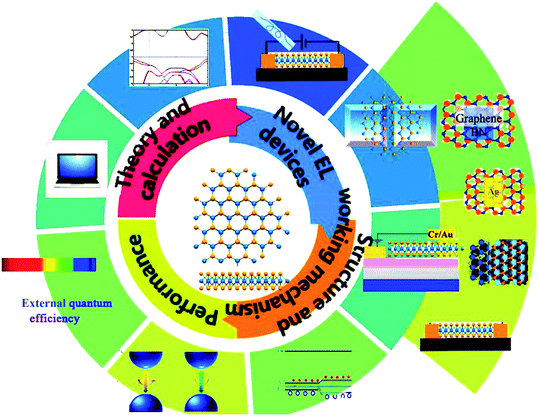 |
| | Fig. 1 The four aspects of light-emitting diodes (LED)-based on TMDCs, namely, theory and calculation, structure and working mechanism, performance, and novel electroluminescence devices. Direction I denotes the theoretical work of TMDCs, including the related semiconductor theory and density function theory calculation. Direction II denotes the structure and working mechanism of LEDs based on TMDCs, including the M–I–S junction, M–S junction, and p–n junction. Direction III denotes the performance of TMDCs-based LEDs, including polarity, color, and external quantum efficiency of the light emission. Direction IV denotes novel EL devices like thermal light-emitting devices and single photon emitters. | |
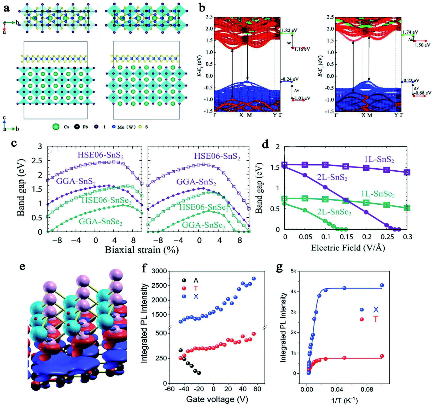
To gain insight into probable applications of TMDCs, it is essential to research their electronic properties such as the bandgap structure, carrier density, and carrier lifetime. According to the Bethe–Salpeter equation, the large difference in electron (me) and hole quality (mh) leads to a small exciton binding energy, thus inducing good optoelectronic properties. The structural, electronic, and optical properties of CsPbI3/MS2 (M = Mo, W) heterostructures were investigated by density functional theory (Fig. 2a and b).37 The differences between the conduction band minimums (conduction band offset, Δc) or valance band maximum (valence band offset, Δv) of the heterostructure are crucial for electron transport or hole blocking.37 To obtain stable CsPbI3/MS2 heterostructures, the binding energies of CsPbI3/MS2 heterostructures were calculated using the formula below:
| | | Eb = (Eheterojunction − Eperovskite − EMS2)/N | (1) |
where
Eheterojunction represents the energies of heterostructures,
Eperovskite and
EMS2 correspond to the energies of the isolated CsPbI
3 surface and monolayer MS
2, respectively. N denotes the interfacial area of CsPbI
3/MS
2 heterostructures. The charge density difference Δ
ρ(Z) along the
Z-direction was characterized as follows:
| | | Δρ(Z) = ρ(Z)total − ρ(Z)perovskite − ρ(Z)MS2 | (2) |
where
ρ(
Z)
total,
ρ(
Z)
perovskite, and
ρ(
Z)
MS2 are the charge densities of the heterostructure, the isolated perovskite surface, and monolayer MS
2, respectively.
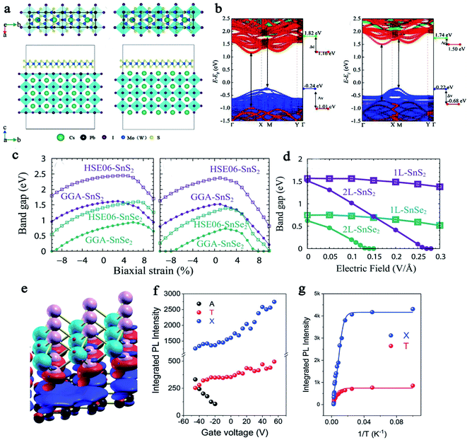 |
| | Fig. 2 (a) Top and side views of CsPbI3/MS2 (M = Mo, W) heterostructures with Pb–I termination (left panel); top and side views of CsPbI3/MS2 heterostructures with Cs–I termination (right panel). (b) Projected band structures of CsPbI3/MoS2 heterostructures with (left panel) Pb–I and (right panel) Cs–I terminations. Green, blue, red and dark yellow points represent the contributions of Pb, I, Mo (W), and S atoms, respectively. The short lines in the right planes are the band edges of the perovskite and MS2 parts of the heterostructures. (a and b) Reproduced with permission;37 Copyright 2019, American Chemical Society. (c) Variations of (left) the band gaps for monolayer SnS2 and SnSe2, (right) the band gaps for bilayer SnS2 and SnSe2 under biaxial compressive and tensile strains. (d) The variation of band gaps as a function of an applied electric field in a normal direction. (c and d) Reproduced with permission;40 Copyright 2019, Elsevier. (e) Changes in the electronic charge densities. The red and blue isosurfaces correspond to charge increase and decrease, respectively. (f) Integrated PL intensity of excitonic emissions as a function of gate voltage. (g) Integrated PL intensity for X and T emissions as a function of inverse of temperature (1/T). (e–g) Reproduced with permission;43 Copyright 2019, Royal Society of Chemistry. | |
The electronic properties of TMDC LEDs can be mediated by the external electric field and external stress. Based on density functional theory, Li et al.38 indicated that the electric field had little influence on the bandgap of the MoS2 monolayer but it can adjust the charge transfer between the MoS2 monolayer and the graphene substrate. Moreover, Hu et al.39 proposed that the weak vertical electric field had little influence on the Eg of MoX2, while the strong one could effectively achieve its modulation of Eg. The band gaps of monolayer SnSe2 slightly increased with the in-plane tensile strains (Fig. 2c).40 A semiconductor-to-metal transition at 10% strain was present for bilayer SnSe2 (Fig. 2c).40 The electrical field perpendicular to the bilayer SnS2 and SnSe2 modulated their electronic bandgap (Fig. 2d). The charge density difference and built-in electric field across the interface of TMDC van der Waals (vdWs) heterostructures prevent photogenerated electron–hole recombination, which goes against the light emission.41 By using first-principles calculations, Zhang et al.42 demonstrated that the MoSe2/WSe2 heterobilayer experienced transitions from type-II to type-I and then to type-II under various external electric fields perpendicular to the layers, which provides great application potential for ultrathin MoSe2/WSe2 heterostructures in future nano-devices and optoelectronics. As shown in Fig. 2e, the charge distribution can be controlled by an external electric field and the light emission properties will vary with the electronic properties (Fig. 2f).43
The light-emission properties of TMDCs can also be manipulated by the working temperature. Li et al.43 investigated intralayer excited-state bi-excitons in graphene/WS2 heterostructures. The binding energy and thermal activation energy of the excited-state biexcitons were obtained to be about 78 and 32 meV, respectively, by temperature-dependent PL intensity analysis, which was further confirmed by theoretical calculations using the stochastic variational method. The PL intensities of trions and bi-excitons as a function of the inverse of temperature were well fitted using the following thermal activation equation (solid lines):
| |  | (3) |
where
I0,
EB, and
kB are the PL intensity at 0 K, the thermal activation energy, and the Boltzmann constant, respectively (
Fig. 2g). The obtained thermal activation energies for trions and bi-excitons were 34 and 32 meV, respectively.
44
3. The structure and working mechanism of TMDC-based LEDs
TMDC-based LEDs have been fabricated in a variety of refined structures, including metal–insulator–semiconductor (MIS) junction, p-type semiconductor/n-type semiconductor (p–n) junction,29 metal–semiconductor (MS) junction.45 Among these structures, the p–n junction of two TMDC layers or TMDC with other routine materials is the key.46 For instance, Ghorai et al.47 fabricated highly luminescent WS2 quantum dots/ZnO heterojunction devices that emit white light.
3.1. MIS junction
TMDC LEDs based on MIS junctions have been extensively reported. Berraquero et al.48 prepared a tunneling diode based on the vertical heterostructure of a single layer of graphene (SLG), hexagonal boron nitride (hBN) layer and a layered WSe2 (Fig. 3a), a single quantum well structure. Without bias voltage between the SLG and the monolayer TMDC, the Fermi energy (EF) of the system is constant across the heterojunction, keeping the net charge from flowing between the layers (Fig. 3b). With a negative bias, the EF of SLG is raised above the minimum of the conduction band (EC) of WSe2. As a result, electrons tunnel from the SLG into the monolayer WSe2, and then tunneling electrons recombine with holes in WSe2 and release light (Fig. 3c). In the MIS junction, the injection of carriers into the semiconductor layer is unipolar.45 A double quantum well structure was reported in another work.49 Clark et al.24 put forward the single-defect LED based on a vertical device constructed by two graphenes separated by WS2 using layered hexagonal boron nitride (BN) barriers (Fig. 3d–f). Liu et al.50 fabricated the vertically assembled double quantum well structure LED using graphene/boron nitride as top and bottom tunneling contacts and monolayer WSe2 as an active light emitter, which increased the probability of radiative recombination as compared to a single quantum well structure. They locally enhanced the EL by integrating a photonic crystal cavity on top of the heterojunction, as shown in Fig. 4a. The enhancement of EL can be attributed to the increase in the spontaneous emission rates of WSe2 by the Purcell effect induced by the photonic crystal cavity.50
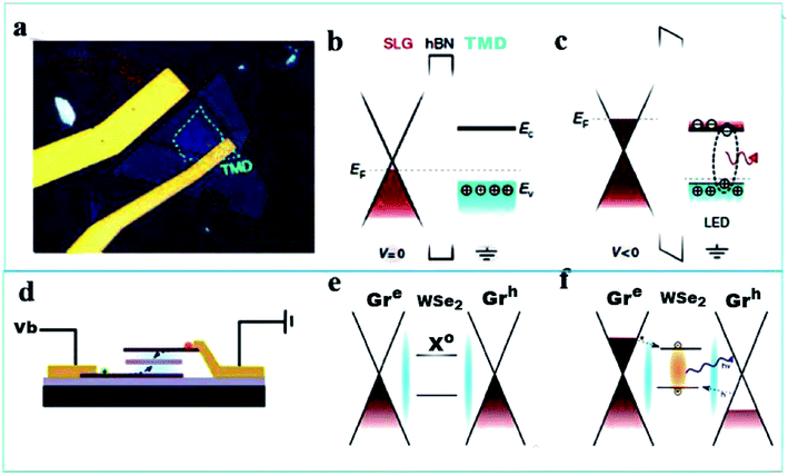 |
| | Fig. 3 (a) Optical microscope image of SLG/BN/WSe2 LED. (b) Band diagram illustration of SLG/BN/WSe2 LED under zero-applied bias. (c) Band diagram illustration of SLG/BN/WSe2 LED under a finite negative bias. (a–c) Reproduced with permission;48 Copyright 2016, Springer Nature. (d) The structure of graphene/WSe2/graphene heterostructure LED. (e) The band diagram illustration of the device under zero-applied bias. (f) The working mechanization of the graphene/BN/WSe2/BN/graphene heterostructure LED under the external bias. (d–f) Reproduced with permission;24 Copyright 2016, American Chemical Society. | |
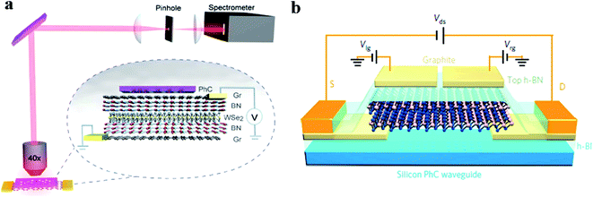 |
| | Fig. 4 Metal–insulator–semiconductor LED integrated with some kind of functional unit. (a) Schematic of light-emitting vdWs heterostructures of the graphene/boron nitride and its integration with a photonic crystal cavity and the EL measurement setup. Reproduced with permission;50 Copyright 2017, American Chemical Society. (b) Schematic of the encapsulated bilayer MoTe2 p–n junction on top of a silicon PhC waveguide. Reproduced with permission;51 Copyright 2017, Springer Nature. | |
The aforementioned works are based on the vertical MIS structure. The following works are based on the paratactic MIS structure. Bie et al.51 demonstrated the MoTe2-based lateral junction with an electrostatic split-gate configuration integrated with a silicon photonic-crystal (PhC) waveguide, as shown in Fig. 4b. The structure can also be seen as the paralleling of two MIS junctions. Remarkably, the device had a grating coupler at the far end of the waveguide to allow excitation and collection. When the device works as an LED, the emitted light near the junction section couples to the waveguide, where it travels in-plane to the grating coupler. As a result, the light emission can be detected near the grating coupler. The integration of TMDC LED with a photonic-crystal provides an effective strategy for enhancing the EL intensity.
3.2. P–n junction (p–i–n junction)
The P–n junction is the most important LED structure. Two kinds of TMDCs can be fabricated as 2D–2D heterojunction diodes. With different band gaps of the p(n) type materials, the p–n junction LED can emit light of different colors.28,52 In general, TMDC-based LEDs cannot emit light in the full visible light range due to the narrow bandgap. The injection of carriers into the semiconductor layer is a bipolar injection in the p–n junction LED.45 Cheng et al.53 created a p–n diode using the p-type monolayer tungsten diselenide (WSe2) and n-type few-layer molybdenum disulfide (MoS2) (Fig. 5a). As for the working mechanism of this LED, the conduction band of MoS2 is below that of WSe2, and the valence band of WSe2 is below that of MoS2. At a small bias voltage, holes can go across the junction, then inject into the MoS2 region and recombine with the electrons, emitting light; the electrons cannot go across the junction (Fig. 5b). At a large bias, the conduction band in MoS2 shifts upward and is higher than that in WSe2; the electrons can go across and are injected into the p-WSe2, while the holes can go across and are injected into the n-MoS2 (Fig. 5c). Therefore, the light intensity undergoes a marked increase with more electron–hole recombination in both WSe2 and MoS2 regions. A scalable, two-step and in situ growth chemical vapor deposition strategy was employed to synthesize self-aligned WSe2–MoS2 monolayer lateral heterojunction arrays and demonstrate their LEDs.54
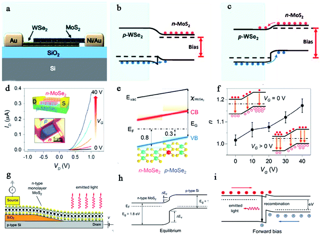 |
| | Fig. 5 Schematic illustration and band diagram of a p–n heterojunction diode. (a) The cross-sectional schematic illustration of the WSe2/MoS2 heterojunction. (b) The ideal band diagram of the WSe2/MoS2 heterojunction under a small forward bias, and (c) under a large forward bias. (a–c) Reproduced with permission;53 Copyright 2014, American Chemical Society. (d) VG-dependent rectifying behavior of the MoSe2 homojunction p–n diode. (e) Energy bandgap schematic for the MoSe2 homojunction. (f) Ideality factor of the MoSe2 homojunction as a function of gate bias. (d–f) Reproduced with permission;55 Copyright 2015, WILEY-VCH. (g) The cross-sectional view of the structure of the MoS2/Si heterojunction LED. (h) Band diagram of the MoS2/Si heterojunction in equilibrium conditions and (i) under forward bias. (h and i) Reproduced with permission; Copyright 2014, American Chemical Society.57 | |
Superior to the heterojunction, the p–n homojunction exhibits ideal diode characteristics (Fig. 5d) because there is no potential discontinuity on the homojunction. In the heterojunction, the tip or notch between the conduction band and the valence band can result in carrier scattering and trap positions near the boundary surface. Jin et al.55 proposed a p–n homojunction based on the p-type Nd-doped MoSe2 and intrinsic n-MoSe2 (Fig. 5e). When the Fermi level moves up at the positive Vg, this ideal diode behavior degenerates. In Fig. 5f, when Vg > 0 V, electron diffusion promotes the increase of the in-band composite current. They assumed that the Fermi levels of p-MoSe2 and n-MoSe2 moved upward with the same energy through the Vg bias.55 Li et al.56 fabricated the MoS2 p–n homojunction by spin-coating AuCl3 and benzyl viologen on MoS2 with post-annealing, respectively. The ultimate thickness of the MoS2 vertical homojunction is 3 nm and the depth of chemical doping is 1.5 nm.
To expand the application range of TMDC LEDs, 2D/3D heterojunction diodes based on TMDC in contact with wide band-gap bulk materials were developed. Lopez-Sanchez et al.57 studied vertical heterojunctions composed of n-type monolayer MoS2 and p-type silicon (Fig. 5g). Because of the difference in electron affinity and bandgap between Si and MoS2, the junction has the characteristics of conduction (δEc = 200 meV) and valence state band shifts (δEv = 900 meV) (Fig. 5h). Under forward bias to the heterojunction, electrons from the n-MoS2 side and holes from p-Si can radiatively recombine in the junction, resulting in light emission. For the valence band and conduction band offset, the valence band and conduction band tip will affect the charge carrier injection efficiency and limit the device current (Fig. 5i). The tunneling diode (p–i–n) composed of a vertical MoS2/SiO2/Si heterostructure was also demonstrated.58 The ionic-liquid gated light-emitting transistor was fabricated on WS2 monolayer and bilayers.59 For TMDCs, the p–n junction can be divided into two kinds: the first one is the vertical p–n junction, which shows large EL intensity for large junction area; the second one is the lateral p–n junction, which shows weaker EL intensity for relatively smaller junction area.
The field-induced p–n junction is an important atomic p–n junction because TMDC possesses atomic thickness and has the potential to be used in microelectronics. Electric field-induced p–n junctions can be used to realize peculiar functionalities in TMDC materials, for which the conventional chemical doping method is difficult to achieve. The field-induced p–n junctions play crucial roles in realizing LED operations as well as circularly polarized EL. Zhang et al.60 fabricated electric field-induced p–n junction and demonstrated that the built-in potential became negative under a forward bias voltage. Baugher et al.61 constructed LEDs based on the field-induced p–n diode on monolayer WSe2. Yumin et al.62 prepared an anion-induced p–n junction based on a WS2/boron nitride heterostructure, which is another method for creating p–n junctions. A 0D–3D p–n diode composed of MoS2 quantum dots and Si was also fabricated to exhibit white light emission from ∼450 nm to 800 nm under forward bias.63 The construction of mixed-dimensional van der Waals heterostructures can take advantage of the different dimensional properties to produce devices with novel functionalities.
3.3. M–S junction
Another type of TMDC LED is based on the M–S junction, which is also called the Schottky diode. Lien et al.64 created an AC voltage pulsed LED based on the Schottky diode of the TMDC monolayer/Au junction. Puchert et al.65 focused on broadband silver EL in Ag/MoS2 nano-LEDs. Due to the low luminescence efficiency of TMDCs LED, several studies were devoted to enhancing the light-emitting performance. Hole injection into the single-layer WSe2 was enhanced by incorporating a metal contact and the EL was enhanced.66 To optimize the device performance of LEDs, the solution-processed MoS2 was used as a hole-injecting electrode, and an electron blocking layer in the form of MoO3 was fabricated.67 A visible organic LED was fabricated using tris(8-hydroxy-quinolinato)aluminum as the emissive layer and MoS2 + PEDOT:PSS as the hole-injection layer, emitting 375 nm electroluminescence with high efficiencies of 8.1 cd A−1 and 5.7 lm W−1.68
4. Luminescence properties of TMDC LEDs
4.1. EL peak location and origin
The luminescence properties of LEDs cover parameters such as EL peak location, EQE, International Lighting Commission chromaticity coordinates (CIE 1931 color diagram), EL polarization, rectifying characteristics, ideality factor, and the switching ratio of the LED p–n junction. The luminescence properties of few-layer TMDC LEDs are reviewed as follows.
Generally, EL is related to the energy bandgap of TMDCs. Light of long wavelength results from narrow bandgap characteristics, and broad bandgap emission will bring out short wavelength light. The EL of TMDC LEDs varies from infrared to green light. The EL peaks of TMDC LEDs are often compared with the PL peak to ascertain the origin.69 In layered TMDCs, the EL is primarily attributed to intrinsic excitons (Xo), charged excitons or trions (X+/X−), free-space emission, and defect-trapped excitons. It is necessary to note that white light emission can be achieved in TMDC-based LEDs by combining TMDC with a broad bandgap semiconductor.
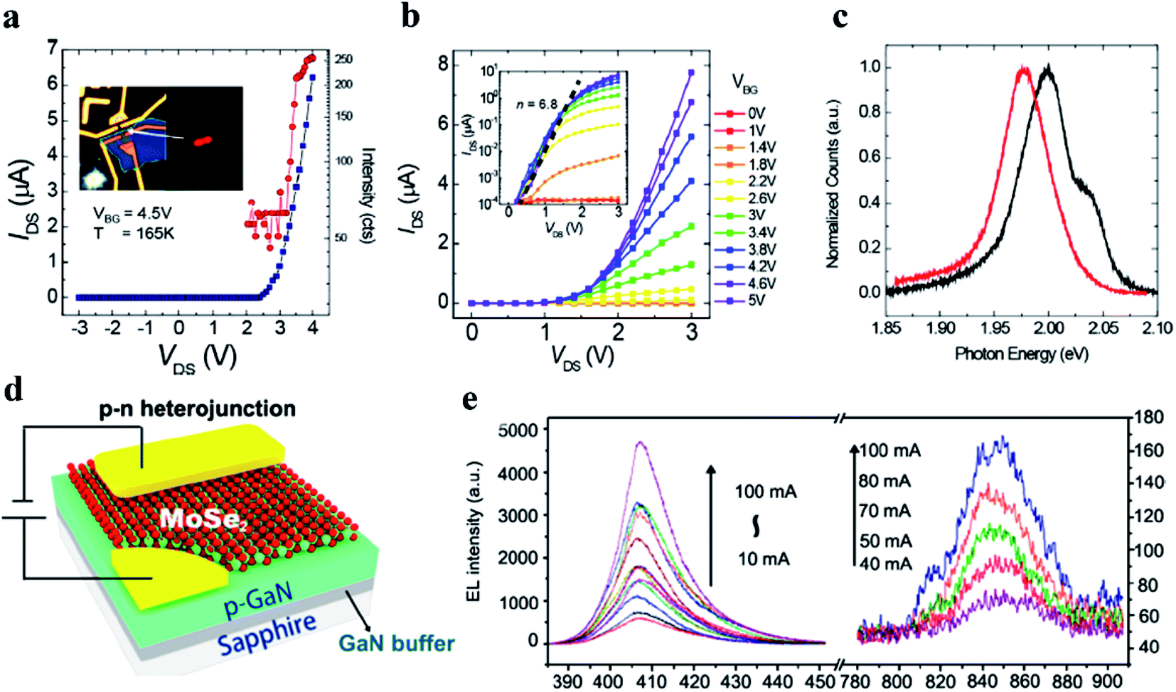
2Monolayer TMDCs can emit light in a highly efficient manner despite being sub-nanometers thick.70 Ross et al.69 observed the EL of a WSe2 monolayer p–n junction at an injection current as low as 200 pA; the EL and PL peaks were consistently located at 1.65 eV (red light) (Fig. 6a). This PL peak is the natural result of the large exciton binding energy of monolayer TMDC due to strong Coulomb interactions, which indicates that in the EL mechanism, the injected electrons and holes form excitons before radiative recombination (Fig. 6b).71,72 With the increase in the injected current, the EL emission intensity increased until it was beyond 2 mA. This is related to the heating effect of the device. Ghorai et al.47 fabricated light-emitting devices of highly luminescent WS2 quantum dots/ZnO heterojunctions (Fig. 6c). Under the injection current of 1.4 mA, the deconvolution of the wide EL spectrum showed three different emission peaks at about 450 nm, 505 nm, and 597 nm. The first peak is the characteristic emission of WS2 nanocrystals, the remaining two peaks are from the emission of defect-related excitons in ZnO (Fig. 6d). Ye et al.73 identified the direct-exciton and bound-exciton recombination process in MoS2/Si LED. The auger recombination of the exciton–exciton annihilation of bound exciton emission was observed.73 Sundaram et al.74 measured the EL of monolayer MoS2 field-effect transistors (Fig. 6e), which showed a peak at ∼685 nm, matching well with the PL peak at ∼680 nm; therefore the EL and PL of that device involved the same excited state, the B exciton (Fig. 6f).
 |
| | Fig. 6 The PL and EL spectral contrast of TMDC-based LEDs in search of the EL peak origin. (a) At 300 K, the EL spectrum (blue) of the monolayer WSe2 p–n junction generated by a current of 5 nA closely resembles the PL spectrum (red). (b) The EL image (red) superimposed on the WSe2 p–n junction device image (grayscale). (a and b) Reproduced with permission;69 Copyright 2014, Springer Nature. (c) The TEM images of the as-synthesized WS2 nanocrystals. Inset is the photo of WS2 nanocrystals suspended in DMF. (d) EL spectra of the Al/PEDOT-PSS/WS2/ZnO/ITO device under different applied currents. Reproduced with permission;47 Copyright 2017, American Chemical Society. (e) EL spectrum of a 1L-MoS2 field effect transistor measured at VD = 5 V and ID = 100 μA. (f) Absorption (Abs), EL, and PL spectra on the same 1L-MoS2. The EL spectrum was measured at VD = 8 V and ID = 164 μA. Reproduced with permission;74 Copyright 2013, American Chemical Society. | |
Importantly, temperature-dependent PL measurements can be used to profoundly probe the EL peak origin. Yang et al.75 measured the EL from the p-Si/i-WS2/n-ITO heterojunction at 77 K; two main emission peaks at 1.950 and 1.985 eV (red light) were detected, as shown in Fig. 7a. A temperature-dependent PL measurement had also been carried out in the temperature range from 81 K to 294 K to trace the emission peaks. The energy of emission peak located at 1.950 and 1.985 eV (red light) matched well with the observed Xb (defect-induced bound exciton) and X− (trion) in the PL spectra at low temperature.75 Multilayer WSe2 emits light more easily than monolayer WSe2 due to its larger light density.76 Schwarz et al.77 measured the typical EL spectra of a single-defect emitter under different applied voltages. A single sharp line at 1.607 eV, labeled SDE1, from the single-defect emitter (SDE) dominated the EL spectrum (Fig. 7b). As shown in Fig. 7c, Pospischil et al.78 showed the EL emission peaks at 1.547 eV of the gate-split WSe2 monolayer LED, which was 93 meV below of PL peak of monolayer WSe2 in energy. The peak shift was assigned to different dielectric environments in both experiments, which influenced the exciton bound energy due to Coulomb screening. In addition, light emission from high-order correlated exciton states was reported in the hBN-encapsulated monolayer WSe2 and WS2 upon bias voltage excitation. The EL was from charged bi-excitons and dark excitons.79
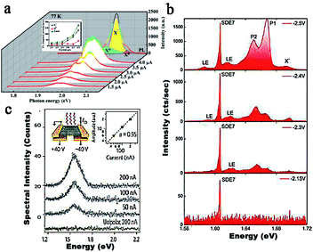 |
| | Fig. 7 Current-dependent EL and temperature-dependent PL spectra of the LED device. (a) EL spectra of the LED device recorded at 77 K under different injection currents. Reproduced with permission;75 Copyright 2016, American Chemical Society. (b) Evolution of EL spectra under different bias. Labels SDE1 and LE are used to denote the EL peaks of the single-defect emitters and other localized states, respectively. Reproduced with permission;77 Copyright 2014, American Association for the Advancement of Science. (c) EL emission spectra of the monolayer WSe2 p–n junction recorded for gate voltages. Reproduced with permission;78 Copyright 2014, Springer Nature. | |
4.1.1. Visible light LED.
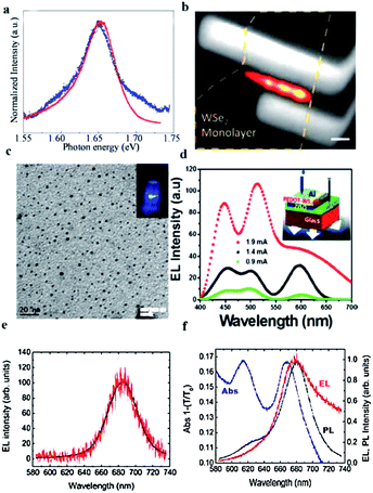
Highly efficient visible light emission is significant for TMDC-based LEDs. Many methods have been adopted to improve the EL of layered TMDC LEDs.23,70,80 Yumin et al.62 realized orange light emission centered at 620 nm from anion induced p–n junction of a WS2/boron nitride heterostructure (Fig. 8a–c). Perumal et al.81 achieved red light from a single layer n-MoS2/SiO2/p-GaN heterostructure device. Chen et al.82 designed an ultrathin MoSe2/GaN heterojunction diode, demonstrating high-intensity EL at 407 nm (violet light) and ∼850 nm (infrared light) (Fig. 8d and e). Ke et al.15 prepared the enhanced EL of CdSe quantum dots coupled with MoS2–chitosan nanosheets. Nikam et al.83 observed white-light-emitting constituents of the p-GaN/p-MoS2/n-MoS2 heterostructure, whose EL spectra consisted of three emission peaks of ∼481 nm (blue light), ∼525 nm (green light), and ∼642 nm (orange light). The device showed the white color purity of CIE (0.41, 0.41). Andrzejewski et al.84 reported red light LED, which was fabricated by embedding a metal–organic (MO-)CVD WS2 monolayer into a vertical p–i–n device architecture of organic and inorganic injection layers. The multicolor LED can be fabricated based on MoS2 QD, and the emission wavelength can be tuned from blue to red by adjusting the thickness of the QD layers.21 The representative visible light LEDs are summarized in Table 1.
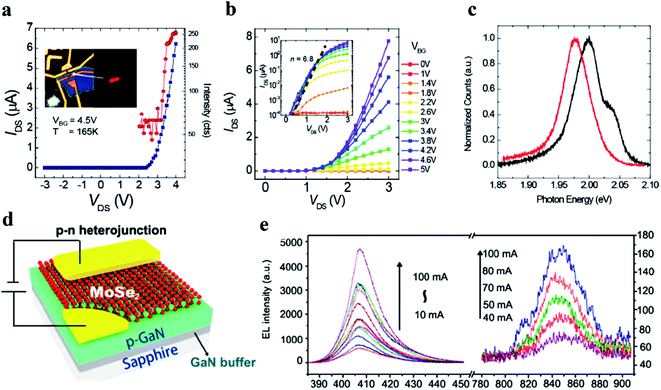 |
| | Fig. 8 The visible light emission of TMDCs-based LEDs. (a) The electrical performance of the TMDCs/boron nitride (BN) heterostructures device under a 4.5 V backgate voltage and 5 V liquid gate voltage at a temperature of 165 K. (b) Electrical properties of the TMDs/boron nitride (BN) heterostructure device under different backgate conditions at 80 K. (c) EL (red) and PL (black) spectra at 80 K under 650 mW m−2 fluence power. (a–c) Reproduced with permission;62 Copyright 2017, John Wiley and Sons. (d) Schematic of the device consisting of an atomic MoSe2 layer on a p-type GaN/sapphire substrate. (e) EL spectra of the n-MoSe2/p-GaN device in the short- and long-wavelength regions. Reproduced with permission;82 Copyright 2016, American Chemical Society. | |
Table 1 The structure composition and luminescence wavelength of visible light light-emitting diodes based on TMDCs
| Structure composition |
Peak position (nm) |
Peak color |
Peak origin |
| MoSe2/GaN82 |
407 |
Violet |
GaN |
| 850 |
Infrared |
MoSe2 |
| P-GaN/p-MoS2/n-MoS2 (ref. 83) |
481 |
Blue |
GaN |
| 525 |
Green |
P–MoS2 |
| 642 |
Orange |
N-MoS2 |
| PEDOT:Poly-PD/WS2/ZnO84 |
650–670 |
Red |
WS2 |
| WS2 quantum dots/ZnO47 |
450 |
Violet |
WS2 |
| 505 |
Green |
ZnO |
| 597 |
Yellow |
ZnO |
| MoS2 QD21 |
470–680 |
Full visible spectrum |
MoS2 |
4.1.2. Infrared light LED.
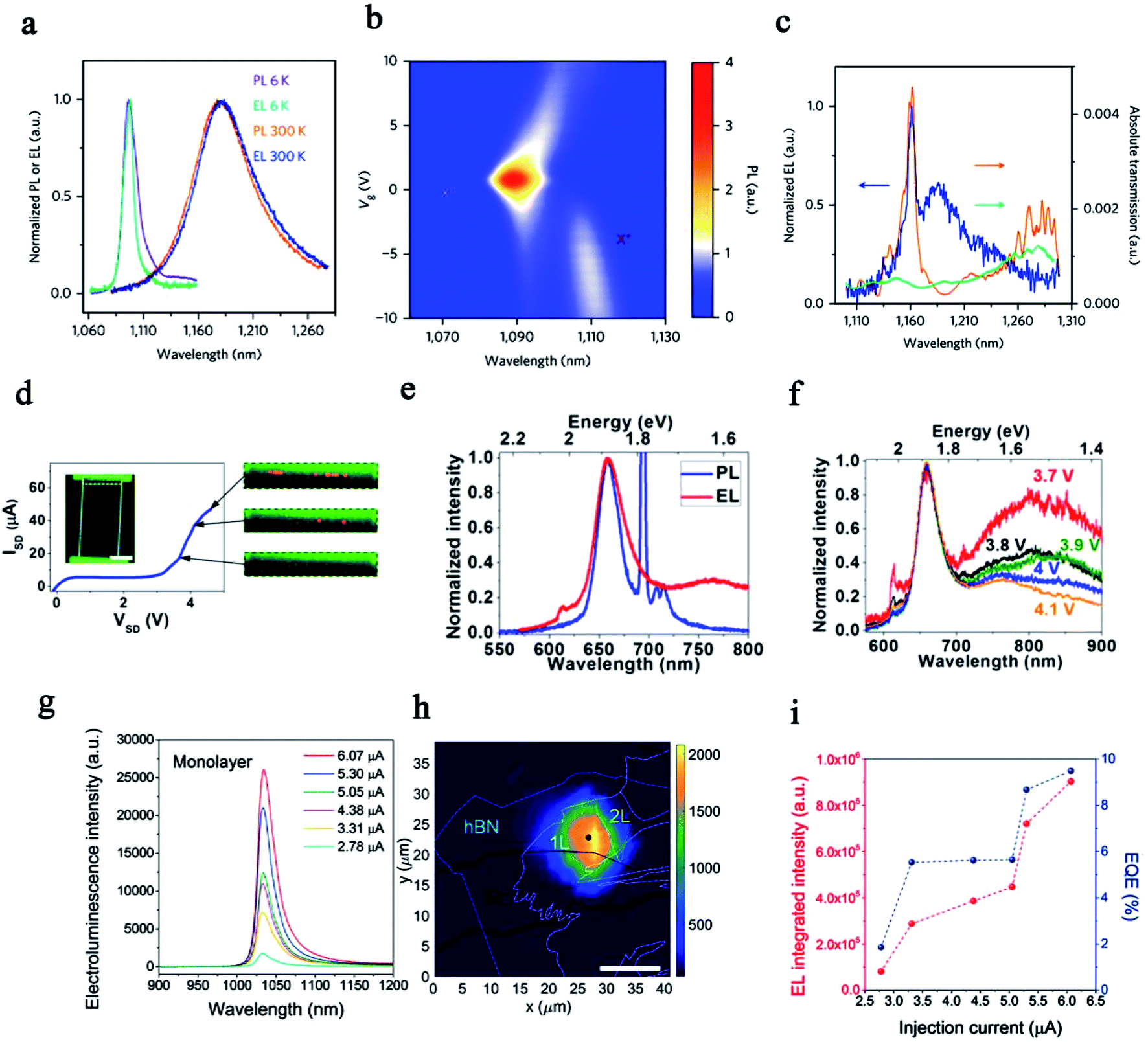
Infrared light LEDs based on TMDCs are easy to construct. The infrared EL peak often originates from direct transitions in monolayer TMDCs or indirect transitions in multilayer TMDCs. Bie et al.51 fabricated a red light LED of the MoTe2 p–n junction, which realized the EL peak of 1090 nm and 1175 nm at cryogenic and room temperatures, respectively. The peaks were due to intrinsic excitons (Xo) of bilayer MoTe2. Both PL and EL peaks demonstrated red shifts at higher recording temperatures (Fig. 9a). The excitonic (Xo) and trionic (X+) peaks can be clearly distinguished in the PL map (Fig. 9b). Moreover, as seen in Fig. 9c, a narrow peak at 1160 nm was on top of a broader peak centered at 1175 nm. The 1160 nm peak was due to the photonic crystal mode, and the 1175 nm peak matched the free-space emission of the bilayer MoTe2. Ponomarev et al.85 found EL in the ionic liquid field-effect transistor based on monolayer MoS2, as shown on the right side of Fig. 9d. The free exciton peak at 660 nm and an additional EL peak were found, as seen in Fig. 9e and f. The additional EL peak was due to the presence of defect states at an energy of 250–300 meV above the top of the valence band, acting as deep traps for holes. Cheng et al.53 found infrared light emission near 880 nm, which was due to the indirect bandgap transition in bilayer WSe2. Interestingly, a significant direct bandgap exciton emission was found in the EL of multilayer MoS2.86 The detection of the 1034.6 nm single EL peak in monolayer MoTe2 LED indicated that the monolayer MoTe2 maintained a high quality after the device fabrication process (Fig. 9g and h).87 The EQE is related to the current injection efficiency (Fig. 9i). A 2D–1D heterostructure of p-type MoS2 nanosheets and n-type CdSe NW was fabricated as an LED, exhibiting electroluminescence at 709 nm.88 Zheng et al.89 found an infrared cathodoluminescence (CL) peak near 1.572 eV via the hBN/WSe2/hBN heterostructure, which corresponded to the exciton energy of monolayer WSe2. The CL of TMDCs has been found by sandwiching between two hBN layers, but the CL of TMDCs was scarcely found by the direct measurement of TMDC materials. It can be concluded that it is still challenging to detect the interband CL signal in monolayer TMDCs, as the electron–hole creation cross-section is extremely small and only a small amount of recombination takes place in the top of the two-dimensional material, most of which takes place in the supporting slab.89 There have been no recent reports on layered TMDC LEDs emitting ultra-violet light, so this may be a problem that needs to be solved.
 |
| | Fig. 9 PL and EL comparison of TMDCs LED. (a) PL and EL spectra of the bilayer MoTe2 flake (the MoTe2 p–n junction) at room temperature and at 6 K. (b) Spectrally resolved PL map of the bilayer MoTe2 at 6 K as a function of gate voltage Vg = Vlg = Vrg. (c) EL and transmission of the waveguide before (orange) and after (green) transfer of MoTe2. (a–c) Reproduced with permission;51 Copyright 2017, Springer Nature. (d) Source–drain current ISD as a function of source–drain bias extending to large VSD values. The inset shows an image of the device with the region of the channel close to the hole injecting contact, where light emission occurs. (e) Comparison of the PL (blue curve) and EL (red curve) spectra (VSD = 4.1 V) measured in the MoS2-based ionic liquid field transistor. (f) Normalized EL spectra recorded for different values of source–drain bias VSD. (d–f) Reproduced with permission;85 Copyright 2015, American Chemical Society. (g) EL spectra from the hBN/monolayer MoTe2/graphite LED under −20 V back gate voltage at 83 K. (h) EL mapping image of the MoTe2 LED device under back gate voltage of −20 V. (i) EL intensity (left) and EQE (right) of monolayer MoTe2 as a function of the injection current. (g–i) Reproduced with permission;87 Copyright 2018, American Chemical Society. | |
4.2. Polarization electroluminescence
Circularly polarized light is involved in various fields ranging from 3D displays to spin sources in spintronics, and information carriers in quantum computation.90,91 There is a strong demand for compact circularly polarized light sources to achieve high integration and controllable polarization.92 Zhang et al.92 first demonstrated WSe2-based ambipolar transistors emitting circularly polarized EL (Fig. 10a). As shown in Fig. 10b–d, the degree of circular polarization EL from the p-Si/i-WS2/n-ITO heterojunction LED device can be modulated simply by the injection current.75 The excitons in monolayer WSe2 forming in the ±K valleys were demonstrated using polarization-resolved PL.69 The excellent matching of the EL peak with the PL peak thus proves that the EL also comes from such valley excitons. The injected electrons and holes form excitons in two valleys, thus producing unpolarized light, as shown in Fig. 10e.75 Zhang et al.60 realized bias voltage-dependent circular polarization in an ionic liquid-gated field effect transistor of a bilayer WSe2 thin flake, as seen in Fig. 10f and g, which possesses a peculiar valleytronic functionality through field-induced WSe2 p–n junction. Ye et al.93 demonstrated the electrically tunable valley polarization in the experiment. By accessing the extra spin degree of freedom (DOF) in electronics, spintronics can be applied for information processes, such as magnetoresistive random-access memory. To realize its potential in electronics, it is necessary to electrically control the valley DOF. These results are not only extremely interesting in physics but could also lead to many practical applications.94
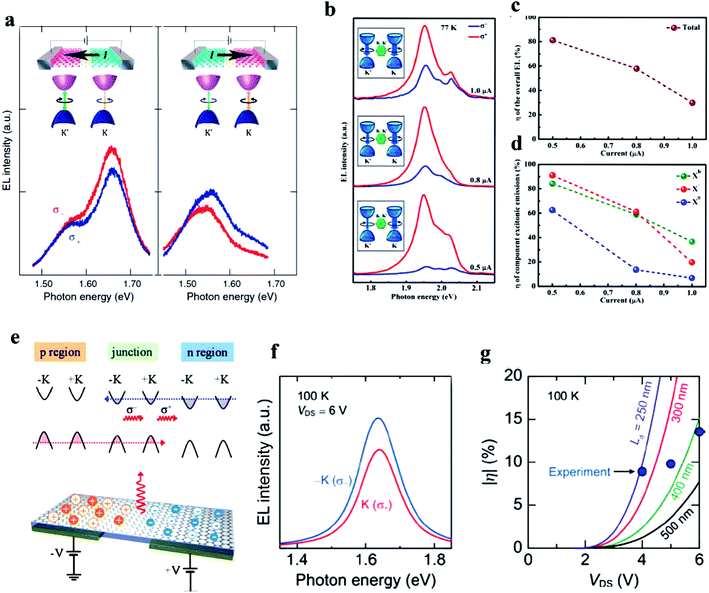 |
| | Fig. 10 Polarization electroluminescence (EL). (a) Circularly polarized EL spectra from p-Si/i-WS2/n-ITO heterojunction ambipolar transistors for two opposite current directions. Reproduced with permission;92 Copyright 2014, American Association for the Advancement of Science. (b) The current-dependent circularly polarized EL spectra from CVD-grown monolayer WS2. (c) Current-dependence of the degree of circularly polarized EL for the overall emission and (d) component neutral excitons Xo, negative trions X−, and bound excitons Xb. (b-d) Reproduced with permission;75 Copyright 2016, American Chemical Society. (e) Band diagram and device schematic of EL generation from valley excitons. Reproduced with permission;69 Copyright 2014, Springer, Nature. (f) Simulated polarized EL spectra from the WSe2 p–n junction. (g) Bias voltage-dependence of the degree of circular polarization in the EL of the WSe2 p–n junction. (f and g) Reproduced with permission;60 Copyright 2017, American Chemical Society. | |
4.3. Ideality factor
Clear current rectification behavior was observed for the WSe2/MoS2 heterojunction (Fig. 11a).53 The ideality factor of the heterojunction device was calculated based on the model of a p–n diode being in series with a resistor (Fig. 11b). In the same heterojunction, the ideality factor of 1.2 was derived with a series resistance of 80 MΩ, at zero gate voltage, but the ideality factor of 3 was derived with a series resistance of 33 MΩ, at −20 V gate voltage.53 The I–V characteristics were evaluated to extract the diode parameters including the reverse saturation current Is and the ideality factor n of diodes by the following formula:| |  | (4) |
where Is is the saturation current derived from the straight line intercept of ln![[thin space (1/6-em)]](https://www.rsc.org/images/entities/char_2009.gif) I at V = 0, as seen in Fig. 11c. q is the electronic charge, V is the applied voltage across the device, n is the diode ideality factor, k is Boltzmann's constant, and T is the absolute temperature.95 From eqn (4), the ideality factor n can be given as
I at V = 0, as seen in Fig. 11c. q is the electronic charge, V is the applied voltage across the device, n is the diode ideality factor, k is Boltzmann's constant, and T is the absolute temperature.95 From eqn (4), the ideality factor n can be given as| |  | (5) |
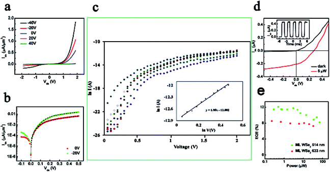 |
| | Fig. 11 (a) Gate-tunable output characteristics of the WSe2/MoS2 heterojunction p–n diode. (b) The ideality factor of the WSe2/MoS2 p–n diode. An ideality factor of 1.2 with a series resistor of 80 MΩ derived at 0 V gate voltage (red circle), and an ideality factor of 1.3 with a series resistor of 33 MΩ was derived at −20 V gate voltage (green triangle). (c) The forward semi-logarithmic I–V relation for the p-Si/n-WS2 heterojunction diode at different thicknesses. The inset shows the lnI vs. lnV plot in the forward region. (c) Reproduced with permission;94 Copyright 2017, Springer Nature. (d) Experimental output (Ids–Vds) characteristic of the vertical heterojunction device in the dark (black) and under the illumination of a laser at wavelength 514 nm with power of 5 mW. The inset denotes the temporal response of the photocurrent generation under 514 nm illumination (10 μW). (e) Power-dependent EQE of the heterojunction device under laser excitation at 514 and 633 nm, at VDS = 0 V and VBG = 0 V. A maximum EQE of 12% was observed. (a, b, d and e) Reproduced with permission;53 Copyright 2014, American Chemical Society. | |
Notably, if n ≈ 1.0, the diode must have ideal diode behavior. This characteristic is due to low charge trap density at the homojunction interface. An ideality factor greater than a unit represents a low-quality connection and is considered a sign of recombination loss.96,97
Kapatel et al.95 studied layer-engineered I–V characteristics of the Si/WS2 van der Waals heterostructure diode. In the 10 μm-thickness WS2 diode, the ideality factor was 2 and the reverse saturated current was 5 × 10⁻¹⁰ A. In terms of the ideality factor, without laser illumination (514 nm, 5 μW) the electronic properties of an ideal diode are much better as compared to homojunction p–n diodes in TMDCs (n ≈ 1.6).56 The output characteristics (Ids–Vds) of the vertical heterojunction with the photovoltaic effect are shown in Fig. 11d. The ideality factor of the current–voltage was 1.64 for the homostructured WSe2 rectifying diode.98
4.4. External quantum efficiency (EQE)
A series of work has been done on the improvement of the QY of TMDC photoluminescence (PL) and the EQE of TMDC LEDs.39,99 Monolayer TMDCs usually experience low QY because of the high density of lattice defects. It is advantageous to increase the QY by overcoming the lattice defects. Unlike conventional semiconductors, the thermal treatment of TMDCs cannot repair the defect but the acid treatment can effectively repair the chalcogen vacancy defect.100 The strong inter-exciton interactions in 1L-TMDCs were considered to be the primary limiting factor of QY.29,101 The strong coulombic interactions between excitons induced an exciton–exciton annihilation (EEA) effect, in which excitons decayed in a nonradiative way.29 Therefore, the density of radiative excitons was reduced. For photodetectors, the photo-to-electronic conversion efficiency is defined as the ratio of the number of carriers collected by electrodes to the number of incident photons.53 The EQE in a MoS2/WSe2 vertical heterojunction can reach 11% under 514 nm laser excitation with a power of 5 μW (Fig. 11e).
For LEDs, the EQE can be evaluated from the ratio of collected EL photon number per second to the injected electron number. The internal quantum efficiency (IQE, ηint) and EQE (ηext) can be calculated using the following equation:
| |  | (6) |
| |  | (7) |
| |  | (8) |
where
Pint denotes the optical power emitted from the active region and can be simplified to the number of photons emitted from the active region per second. P denotes the optical power emitted into free space and can be simplified to the number of photons emitted into free space per second.
I denotes the injection current and can be simplified to the number of electrons injected into the LED per second.
87ηext denotes the extraction efficiency or external quantum efficiency, and can be an indicator of the limitations of high-performance LEDs; it is often lower than 50%. To date, the EQE of LEDs based on TMDCs is relatively low.
51,53 The maximum EQE of 12% was achieved in the monolayer WSe
2/MoS
2 p–n diode.
50 The EQE reached 9.5% from LED on the graphene–hBN–MoTe
2 heterostructure.
87 The EQE of MoS
2 and MoSe
2 light-emitting quantum wells decreased on going from cryogenic conditions to room temperature.
102 On the contrary, the EQE of WSe
2 light-emitting quantum wells increased with temperature. The EQE of the WSe
2 light-emitting quantum wells reached 5%, which was much larger than the EQE of MoS
2 and MoSe
2 light-emitting quantum wells in ambient conditions. A performance outline of TMDC LEDs is given in
Table 2.
Table 2 Summary of performance of layered TMDCs LED, in terms of material configuration, EL peak position, ideality factor, and external quantum efficiency (EQE)
| Material configuration |
EL peak position |
Origin of peak |
Ideal factor |
EQE |
Literature |
| P+-Si/i-WS2/n-ITO |
1.950 and 1.985 eV |
Bound exciton and trion peak of WS2 |
— |
— |
Yang et al.73 |
| Bilayer MoTe2–silicon |
1175 nm/1160 nm |
Free-space emission of the bilayer MoTe2/photonic crystal mode |
— |
0.5% at 1160 nm |
Bie et al.52 |
| Graphene/hBN/MoTe2 |
1034.6 nm |
Exciton of MoTe2 |
|
9.5% at 83 K |
Zhu et al.85 |
| P-Monolayer WSe2/n-MoS2 junction |
A (792 nm) and B (626 nm) |
Exciton of WSe2 and exciton of MoS2 |
1.2 |
A maximum of 12%, 0.5 μW |
Li et al.56 |
| A' (546 nm) and B′ (483 nm) |
Hot electron peak |
| I (880 nm) |
Indirect band gap emission |
| Graphene/BN/WSe2/BN/graphene |
1.651–1.71 eV (621–598 nm) |
Defect-bound excitons |
— |
— |
Clark et al.24 |
| 1.72 and 1.75 eV (595–585 nm) |
Charged and neutral intrinsic excitons |
| Monolayer WSe2 p–n junction |
1.69 eV (606 nm) |
Xo recombination |
— |
IQE = 5% |
Ross et al.67 |
| 1.663 eV to 1.625 eV |
X− trion (two electrons and one hole) |
| 1.670 eV (613 nm) |
X+ trion (two holes and one electron) |
| 1.59 eV (644 nm) |
Impurity-bound excitons (XI) |
| N–MoS2/p-Si |
694 nm |
Intrinsic peak of MoS2 |
— |
4.4% |
Sanchez et al.58 |
| 644 nm |
The heterojunction region |
| 721 nm |
Trion resonance of MoS2 |
| Mono- and bilayer WS2 ionic liquid gated FETs |
1.95 eV (525 nm) |
Direct transition |
— |
— |
Jo et al.97 |
| 1.7 eV (602 nm) |
Indirect transition |
| Monolayer WSe2 p–n junction |
752 nm |
Direct-gap exciton transition |
1.9 |
0.2% at 522 nm |
Baugher et al.55 |
| Graphene/BN/WSe2/BN/Graphene |
738.7 nm |
Xo recombination |
1.14 |
Below 0.2% |
Liu et al.50 |
| 759 nm |
X−/X+ impurity exciton peak |
5. Novel LED devices
5.1. Single-photon emitter
Recently, significant progress has been made in realizing efficient single-photon emitters that can be used for quantum information and technology devices. Single-defects in monolayer TMDCs may be a new type of single-photon source.103–106 Clark et al.24 demonstrated a single-defect emitter by using both vertical and lateral van der Waals heterostructures of monolayer WSe2. Single-defect emitters are enabled by integration with a variety of optical components such as photonic crystal cavities and waveguides (Fig. 12a).50 Liu et al.50 demonstrated direct modulation of this single-mode EL at a high speed of ∼1 MHz, as seen in Fig. 12b. The high-resolution PL spectrum of the 1L-WSe2 flake revealed a doublet split by Δ = 726 meV with unequal intensities, as shown in Fig. 12c.106 A strong antibunched photon emission from this emitter was observed and then confirmed by fit using the relation g(2)(τ) = 1 − ρ2e−|τ|/T (Fig. 12d).107 The coupling single photons were detected from discrete quantum emitters in WSe2, which was also verified via the observation of antibunching in the signal (g(2)(0) = 0.42).108 To date, much research has been conducted on single-photon emitters of layered TMDCs utilizing PL; however, little has been done by way of EL. Iff et al.109 showed a compact and hybrid two-dimensional semiconductor-piezoelectric device that allows for controlling the energy of single photons emitted and localized in wrinkled WSe2 monolayers by strain fields (Fig. 12e).109 The ensemble emission due to defect-bound excitonic complexes can be seen in both 1L and 2L WSe2 (Fig. 12f).107 The realization of electrically driven polariton LEDs in atomically thin semiconductors at room temperature presents a promising step towards achieving an inversionless electrically driven laser, as well as ultrafast microcavity LEDs.110
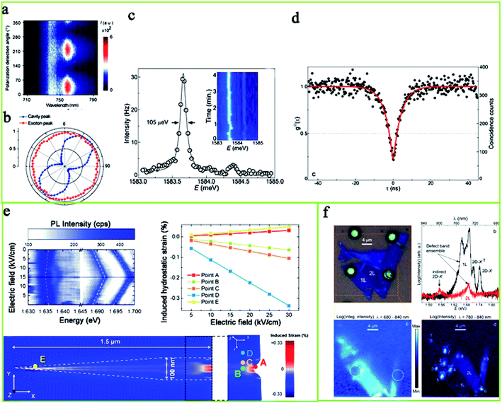 |
| | Fig. 12 The performance of a single photon emitter based on layered TMDCs. (a) The measured on-cavity EL as a function of polarization detection angle. (b) Normalized cavity-enhanced peak intensity (blue dots) and exciton peak intensity (red dots) as a function of polarization detection angle. (a and b) Reproduced with permission;50 Copyright 2017, American Chemical Society. (c) High-resolution PL spectrum of 0D-X from the location of WSe2 on the p-Si substrate. (d) Normalized second-order correlation function g(2)(τ) of the 0D-X lines of WSe2 on the p-Si substrate under non-resonant cw excitation at P = 0.5PN. (e) Contour plot of the PL spectra of SPEs as a function of the electric field applied on a (001) piezoelectric device. Evolution of the hydrostatic strain as a function of the electric field applied to a (001) piezoelectric device calculated on five different points of the wrinkle. Reproduced with permission;109 Copyright 2019, American Chemical Society. (f) Typical PL emission spectra for 1L (black) and 2L (red) WSe2 from the smooth and unstrained locations of the flake; color-coded spatial maps of PL with (left) integrated intensities in the spectral range of 680–840 nm, and (right) intensities in the spectral range of 780–840 nm. (c, d and f) Reproduced with permission;107 Copyright 2015, American Chemical Society. | |
5.2. AC voltage transient EL in TMDCs
Lien et al.64 demonstrated a transient-mode EL device based on TMDC monolayers (including MoS2, WS2, MoSe2, and WSe2). The device structure was MS heterojunction, as shown in Fig. 13a. Pulsed EL was observed at each Vg transition (Fig. 13b). EL from this device was weakly dependent on the Schottky barrier height or polarity. The main factor limiting the performance of the time-EL device is QY droop due to bi-excitonic recombination. The large voltage drop and the steep energy band bending at the Schottky contact lead to large transient tunneling currents. Injected electrons diffused inward while holes exited the semiconductor through contact or recombination with incoming electrons. In the steady-state, the band bending and tunneling current of the semiconductor and contact decrease. In the alternating current transient process, the excess electron and hole population occur simultaneously. The transient EL was applied to display the letters C–A–L (Fig. 13c). It is rewarding that suspended two-dimensional materials can produce periodic oscillation in the reflection and PL spectra, therefore providing a direct way to fabricate periodic EL devices.111 Recently, a transient-mode EL device was been fabricated based on WS2-metal contact; a centimeter-scale (≈0.5 cm2) visible (640 nm) display was demonstrated, which showcases the potential of TMDC systems for display applications.112
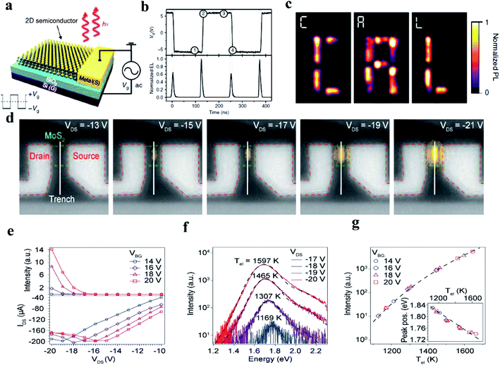 |
| | Fig. 13 AC voltage transient EL and thermal light emission from layered TMDCs. (a) Structure diagram of the time-EL device. (b) Time-resolved EL. (c) Operation of the seven-segment display of C–A–L. (a–c) Reproduced with permission.64 Copyright 2018, Springer Nature. (d) Optical images of the thermal light emitter for various bias conditions, ranging from VDS = −13 to −21 V (from left to right). (e) Integrated thermal emission intensity and corresponding current IDSversus bias voltage VDS plots. (f) Measured thermal emission spectra. (g) Thermal light emission intensity plotted as a function of temperature. (d–g) Reproduced with permission;113 Copyright 2017, WILEY-VCH. | |
5.3. Thermal light emission
Thermoluminescence occurs from a nanomaterial at elevated temperatures, which leads to the thermal propagation of exciton states and the subsequent radiative recombination.45 High temperatures can be reached by minimizing heat loss in the vertical direction through the substrate or along the lateral direction toward the contact electrodes. The transverse heat flux is determined by the thermal conductivity of the material.113 Dobusch et al.113 demonstrated that a MoS2 monolayer sheet, freely suspended in a vacuum over a distance of 150 nm, emitted visible light as a result of Joule heating (Fig. 13d). Due to the poor transfer of heat to the contact electrodes, as well as the suppressed heat dissipation through the underlying substrate, the electron temperature can reach 1500–1600 K, as seen in Fig. 13e and f.6,113,114 The well-pronounced peak at around 1.7 eV corresponds to the A-exciton of the MoS2 monolayer. The second (weaker) peak at higher energy, referring to the B-exciton, arises from the spin–orbit splitting of the valence band and corresponds to the transition from the lower spin level of the valence band (Fig. 13g). Compared to the PL spectra, the thermal emission spectra are usually broader and shifted in energy.
6. Conclusions
Since the EL light intensity and luminescence power of 2D layered TMDCs LEDs is low, it is essential to improve the emission performance of TMDCs LED. It is important to design effective structures to extend the multifunction of TMDC LEDs. Nowadays, the highest EQE of TMDC LEDs is only 12%, which reduces the utilization rate of TMDCs. The low EQE originates from the low quantum yield (QY). It is necessary to take measures to improve the QY of TMDCs. The QY of monolayer MoS2 was hugely enhanced by organic superacid treatment.115 This method opens the door for the development of highly efficient LEDs. Hot carriers can be injected into the bandgap of the heterojunction, then electrons may be trapped or form an interfacial state. Therefore, to improve the reliability of electronic devices based on TMDCs, thermal management may be necessary.113 Otherwise, the control of valley-spin polarization in solids is a basic research area for electronic applications. Further studies on polarization EL are necessary.
The optical band gap of monolayer TMDCs is so narrow that the EL peak wavelength is in the range from infrared light to red light. In order for layered TMDCs heterostructure LEDS to emit visible light in the full spectrum range, they need to be assembled with other wide bandgap materials. Moreover, as a supplement to sunlight, white light is useful in agriculture, for example, in greenhouse plants. It is rare to emit white light from TMDCs LEDs up to ultraviolet light, so TMDC-based white light LEDs may be an important research direction.116,117 Haldar et al.118 have found white light in MoS2 QD PL, which provides instructions for the fabrication of white light LEDs in the future. Furthermore, flexible devices are expected to meet the increasing demands for wearable and portable electronics. MoS2-dependent flexible optoelectronic devices have been fabricated,119–122 so it may be interesting to prepare flexible LEDs based on TMDCs. MoS2 with piezo-phototronic effects has been fabricated, which indicates a new direction for the study of other TMDC piezo-phototronic devices.123 MoS2 materials have also been used in gas sensors and nanogenerators; this is a potential direction for integrating 2D layered TMDCs LED with other devices such as gas sensors, nanogenerators.122,124,125
Conflicts of interest
There are no conflicts of interest to declare.
Acknowledgements
We acknowledge support from the National Natural Science Foundation of China (Grant No. 51705138, 11874025 and 11674113).
Notes and references
- G. G. D. Han, K. H. Tu, F. Niroui, W. Xu, S. Zhou, X. Wang, V. Bulović, C. A. Ross, J. H. Warner and J. C. Grossman, Adv. Funct. Mater., 2017, 27, 1703688 CrossRef.
- N. T. Son, Y.-S. Kim and E. Janzén, Phys. Status Solidi RRL, 2015, 9, 707–710 CrossRef CAS.
- D. Chiappe, I. Asselberghs, S. Sutar, S. Iacovo, V. Afanas'ev, A. Stesmans, Y. Balaji, L. Peters, M. Heyne, M. Mannarino, W. Vandervorst, S. Sayan, C. Huyghebaert, M. Caymax, M. Heyns, S. De Gendt, I. Radu and A. Thean, Adv. Mater. Interfaces, 2016, 3, 1500635 CrossRef.
- D. Arcos, D. Gabriel, D. Dumcenco, A. Kis and N. Ferrer-Anglada, Phys. Status Solidi B, 2016, 253, 2499–2504 CrossRef CAS.
- H. J. Kim, D. Kim, S. Jung, M. H. Bae, Y. J. Yun, S. N. Yi, J. S. Yu, J. H. Kim and D. H. Ha, J. Raman Spectrosc., 2018, 49, 1938–1944 CrossRef CAS.
- H. S. Tsai, Y. H. Huang, P. C. Tsai, Y. J. Chen, H. Ahn, S. Y. Lin and Y. J. Lu, ACS Omega, 2020, 5, 10725–10730 CrossRef CAS PubMed.
- R. Caputo, A. Tekin, R. Nesper and Z. Anorg, Z. Anorg. Allg. Chem., 2019, 645, 309–316 CrossRef CAS.
- J. B. Cook, H. Kim, T. C. Lin, C. H. Lai, B. Dunn and S. H. Tolbert, Adv. Energy Mater., 2017, 7, 1601283 CrossRef.
- G. J. Choi, Q. Van Le, K. S. Choi, K. C. Kwon, H. W. Jang, J. S. Gwag and S. Y. Kim, Adv. Mater., 2017, 29, 1702598 CrossRef PubMed.
- E. G. da Silveira Firmiano, A. C. Rabelo, C. J. Dalmaschio, A. N. Pinheiro, E. C. Pereira, W. H. Schreiner and E. R. Leite, Adv. Energy Mater., 2014, 4, 1301380 CrossRef.
- G. Froehlicher, E. Lorchat and S. Berciaud, Phys. Rev. B, 2016, 94, 085429 CrossRef.
- H. Coy-Diaz, F. Bertran, C. Chen, J. Avila, J. Rault, P. Le Fèvre, M. C. Asensio and M. Batzill, Phys. Status Solidi RRL, 2015, 9, 701–706 CrossRef CAS.
- C. Wang, Y. Zhan and Z. Wang, ChemistrySelect, 2018, 3, 1713–1718 CrossRef CAS.
- J. Shi, R. Tong, X. Zhou, Y. Gong, Z. Zhang, Q. Ji, Y. Zhang, Q. Fang, L. Gu, X. Wang, Z. Liu and Y. Zhang, Adv. Mater., 2016, 28, 10664–10672 CrossRef CAS PubMed.
- R. Ke, X. Zhang, L. Wang, C. Zhang, S. Zhang, H. Niu, C. Mao, J. Song, B. Jin and Y. Tian, J. Solid-State Electron Devices, 2015, 19, 1633–1636 CrossRef CAS.
- M. Shrivastava, R. Kumari, M. R. Parra, P. Pandey, H. Siddiqui and F. Z. Hague, Opt. Mater., 2017, 73, 763–771 CrossRef CAS.
- W. Su, Y. Wang, W. Wu, H. Qin, K. Song, X. Huang, L. Zhang and D. Chen, J. Mater. Chem. C, 2017, 5, 6352–6358 RSC.
- Y. M. Liu, J. J. Yang, J. T. Cao, J. J. Zhang, Y. H. Chen and S. W. Ren, Sens. Actuators, B, 2016, 232, 538 CrossRef CAS.
- F. Xu, B. Zhu, B. Cheng, J. Yu and J. Xu, Adv. Opt. Mater., 2018, 6, 1800911 CrossRef.
- K. Mallikarjuna, M. A. Shinde and H. Kim, Mater. Sci. Semicond. Process., 2020, 117, 105176 CrossRef CAS.
- W. Yin, X. Bai, X. Zhang, J. Zhang, X. Gao and W. W. Yu, Part. Part. Syst. Charact., 2019, 36, 1800362 CrossRef.
- A. Capasso, F. Matteocci, L. Najafi, M. Prato, J. Buha, L. Cinà, V. Pellegrini, A. D. Carlo and F. Bonaccorso, Adv. Energy Mater., 2016, 6, 1600920 CrossRef.
- Y. Chen, X. Wang, G. Wu, Z. Wang, H. Fang, T. Lin, S. Sun, H. Shen, W. Hu, J. Wang, J. Sun, X. Meng and J. Chu, Small, 2018, 14, 1703293 CrossRef PubMed.
- G. Clark, J. R. Schaibley, J. Ross, T. Taniguchi, K. Watanabe, J. R. Hendrickson, S. Mou, W. Yao and X. Xu, Nano Lett., 2016, 16, 3944–3948 CrossRef CAS PubMed.
- S. Qiao, R. Cong, J. Liu, B. Liang, G. Fu, W. Yu, K. Ren, S. Wang and C. Pan, J. Mater. Chem. C, 2018, 6, 32–33 Search PubMed.
- X. Zhou, N. Zhou, C. Li, H. Y. Song, Q. Zhang, X. Z. Hu, L. Gan, H. Q. Li, J. T. Lü, J. Luo, J. Xiong and T. Y. Zhai, 2D mater., 2017, 4, 025048 CrossRef.
- N. Krane, C. Lotze, J. M. Lager, G. Reecht and K. J. Franke, Nano Lett., 2016, 16, 5163–5168 CrossRef CAS PubMed.
- H. Jeong, R. Salas-Montiel, G. Lerondel and M. S. Jeong, J. Alloys Compd., 2017, 708, 612–618 CrossRef CAS.
- Y. Lee and J. Kim, ACS Photonics, 2018, 5, 4187–4194 CrossRef CAS.
- M. Farkous, M. Bikerouin, H. T. T. Phung, M. El-Yadri, E. Feddi, F. Dujardin, C. A. Duque, D. Muoi, H. V. Phuc, C. V. Nguyen and N. N. Hieu, Mater. Res. Express, 2019, 6, 065060 CrossRef CAS.
- K. Ren, M. Sun, Y. Luo, S. Wang, Y. Xu, J. Yu and W. Tang, Phys. Lett. A, 2019, 383, 1487–1492 CrossRef CAS.
- C. B. Qin, Y. Gao, Z. X. Qiao, L. T. Xiao and S. T. Jia, Adv. Opt. Mater., 2016, 4, 1429–1456 CrossRef CAS.
- M. Hong, X. B. Zhou, N. Gao, S. L. Jiang, C. Y. Xie, L. Y. Zhao, Y. Gao, Z. P. Zhang, P. F. Yang, Y. P. Shi, Q. Zhang, Z. F. Liu, J. J. Zhao and Y. F. Zhang, ACS Nano, 2018, 12, 10095–10103 CrossRef CAS PubMed.
- Y. Ge, Z. Y. Ding, W. J. Meng, J. H. Wang, Y. B. Hou, G. Wu, Q. Y. Lu and X. P. Yang, Phys. Rev. B, 2020, 101, 104305 CrossRef CAS.
- F. Bussolotti, J. W. Chai, M. Yang, H. Kawai, Z. Zhang, S. J. Wang, S. L. Wong, C. Manzano, Y. L. Huang, D. Z. Chi and K. E. J. Goh, RSC Adv., 2018, 8, 7744–7752 RSC.
- F. Zhang, Z. X. Lu, Y. C. Choi, H. N. Liu, H. S. Zheng, L. M. Xie, K. Park and L. Y. Jiao, ACS Appl. Nano Mater., 2018, 1, 2041–2048 CrossRef CAS.
- J. He, J. Su, Z. Lin, S. Zhang, Y. Qin, J. Zhang, J. Chang and Y. Hao, J. Phys. Chem. C, 2019, 123, 7158–7165 CrossRef CAS.
- X. Liu, Z. Li and J. Phys, Chem. Lett., 2015, 6, 3269–3275 CAS.
- X. Hu, Q. Zhang and S. Yu, Appl. Surf. Sci., 2019, 478, 857–865 CrossRef CAS.
- A. Rahman, H. J. Kim, M. Noor-A-Alam and Y.-H. Shin, Curr. Appl. Phys., 2019, 19, 709–714 CrossRef.
- A. T. Hanbicki, H. J. Chuang, M. R. Rosenberger, C. S. Hellberg, S. V. Sivaram, K. M. McCreary, I. I. Mazin and B. T. Jonker, ACS Nano, 2018, 12, 4719–4726 CrossRef CAS PubMed.
- F. Zhang, W. Li and X. Q. Dai, Solid State Commun., 2017, 266, 11–15 CrossRef CAS.
- Y. Li, N. Stolte, B. K. Li, H. Li, G. H. Cheng, D. Pan and J. N. Wang, Nanoscale, 2019, 11, 13552–13557 RSC.
- S. Y. Chen, T. Goldstein, T. Taniguchi, K. Watanabe and J. Yan, Nat. Commun., 2018, 9, 3717 CrossRef PubMed.
- J. Wang, I. Verzhbitskiy and G. Eda, Adv. Mater., 2018, 30, 1802687 CrossRef PubMed.
- K. Zhang, M. Peng, W. Wu, J. Guo, G. Gao, Y. Liu, J. Kou, R. Wen, Y. Lei, A. Yu, Y. Zhang, J. Zhai and Z. L. Wang, Mater. Horiz., 2017, 4, 274–280 RSC.
- A. Ghorai, S. Bayan, N. Gogurla, A. Midya and S. K. Ray, ACS Appl. Mater. Interfaces, 2017, 9, 558–565 CrossRef CAS PubMed.
- C. Palacios-Berraquero, M. Barbone, D. M. Kara, X. Chen, I. Goykhman, D. Yoon, A. K. Ott, J. Beitner, K. Watanabe, T. Taniguchi, A. C. Ferrari and M. Atature, Nat. Commun., 2016, 7, 12978 CrossRef CAS PubMed.
- Y. W. Sheng, T. X. Chen, Y. Lu, R. J. Chang, S. Sinha and J. H. Warner, ACS Nano, 2019, 4, 4530–4537 CrossRef PubMed.
- C. H. Liu, G. Clark, T. Fryett, S. f. Wu, J. J. Zheng, F. Hatami, X. D. Xu and A. Majumdar, Nano Lett., 2017, 17, 200–205 CrossRef CAS PubMed.
- Y. Q. Bie, G. Grosso, M. Heuck, M. M. Furchi, Y. Cao, J. Zheng, D. Bunandar, E. Navarro-Moratalla, L. Zhou, D. K. Efetov, T. Taniguchi, K. Watanabe, J. Kong, D. Englund and P. Jarillo-Herrero, Nat. Nanotechnol., 2017, 12, 1124–1129 CrossRef CAS PubMed.
- F. Xue, L. Yang, M. Chen, J. Chen, X. Yang, L. Wang, L. Chen, C. Pan and Z. L. Wang, NPG Asia Mater., 2017, 9, e418 CrossRef CAS.
- R. Cheng, D. Li, H. Zhou, C. Wang, A. Yin, S. Jiang, Y. Liu, Y. Chen, Y. Huang and X. Duan, Nano Lett., 2014, 14, 5590–5597 CrossRef CAS PubMed.
- M. Y. Li, J. Pu, J. K. Huang, Y. H. Miyauchi and K. Matsuda, Adv. Funct. Mater., 2018, 28, 1706860 CrossRef.
- Y. Jin, D. H. Keum, S. J. An, J. Kim, H. S. Lee and Y. H. Lee, Adv. Mater., 2015, 27, 5534–5540 CrossRef CAS PubMed.
- H. M. Li, D. Lee, D. Qu, X. Liu, J. Ryu, A. Seabaugh and W. J. Yoo, Nat. Commun., 2015, 6, 6564 CrossRef CAS PubMed.
- O. L. Sanchez, E. A. Llado, V. Koman, A. F. Morral, A. Radenovic and A. Kis, ACS Nano, 2014, 8, 3042–3048 CrossRef PubMed.
- K. Nishiguchi, A. Castellanos-Gomez, H. Yamaguchi, A. Fujiwara, H. S. J. van der Zant and G. A. Steele, Appl. Phys. Lett., 2015, 107, 053101 CrossRef.
- S. Jo, N. Ubrig, H. Berger, A. B. Kuzmenko and A. F. Morpurgo, Nano Lett., 2014, 14, 2019–2025 CrossRef CAS PubMed.
- Y. Zhang, R. Suzuki and Y. Iwasa, ACS Nano, 2017, 11, 12583–12590 CrossRef CAS PubMed.
- B. W. Baugher, H. O. Churchill, Y. Yang and P. Jarillo-Herrero, Nat. Nanotechnol., 2014, 9, 262–267 CrossRef CAS PubMed.
- A. A. El Yumin, J. Yang, Q. Chen, O. Zheliuk and J. Ye, Phys. Status Solidi B, 2017, 254, 1700180 CrossRef.
- S. Mukherjee, R. Maiti, A. K. Katiyar, S. Das and S. K. Ray, Sci. Rep., 2016, 6, 29016 CrossRef CAS PubMed.
- D. H. Lien, M. Amani, S. B. Desai, G. H. Ahn, K. Han, J. H. He, J. W. Ager III, M. C. Wu and A. Javey, Nat. Commun., 2018, 9, 1229 CrossRef PubMed.
- R. P. Puchert, F. Steiner, G. Plechinger, F. J. Hofmann, I. Caspers, J. Kirschner, P. Nagler, A. Chernikov, C. Schuelle, T. Korn, J. Vogelsang, S. Bange and J. M. Lupton, Nat. Nanotechnol., 2017, 12, 637–641 CrossRef CAS PubMed.
- X. Zhang, W. Guo, Z. Wang, H. Ke, W. Zhao, A. Zhang, C. Huang and N. Jia, Sens. Actuators, B, 2017, 253, 470–477 CrossRef CAS.
- K. J. Reynolds, J. A. Barker, N. C. Greenham, R. H. Friend and G. L. Frey, J. Appl. Phys., 2002, 92, 7556–7563 CrossRef CAS.
- X. W. Zhang, W. S. Li, Z. T. Ling, Y. Zhang, J. W. Xu, H. Wang, G. H. Chen and B. Wei, J. Mater. Chem. C, 2019, 7, 926–936 RSC.
- J. S. Ross, P. Klement, A. M. Jones, N. J. Ghimire, J. Yan, D. G. Mandrus, T. Taniguchi, K. Watanabe, K. Kitamura, W. Yao, D. H. Cobden and X. Xu, Nat. Nanotechnol., 2014, 9, 268–272 CrossRef CAS PubMed.
- G. Gupta and K. Majumdar, Phys. Rev. B, 2019, 99, 085412 CrossRef CAS.
- I. Gutierrez-Lezama, B. A. Reddy, N. Ubrig and A. F. Morpurgo, 2D Mater., 2016, 3, 045016 CrossRef.
- Y. Rong, Y. Sheng, M. Pacios, X. Wang, Z. He, H. Bhaskaran and J. H. Warner, ACS Nano, 2016, 10, 1093–1110 CrossRef CAS PubMed.
- Y. Ye, Z. Ye, M. Gharghi, X. Yin, H. Zhu, M. Zhao and X. Zhang, Appl. Phys. Lett., 2014, 104, 193508 CrossRef.
- R. S. Sundaram, M. Engel, A. Lombardo, R. Krupke, A. C. Ferrari, P. Avouris and M. Steiner, Nano Lett., 2013, 13, 1416–1421 CrossRef CAS PubMed.
- W. Yang, J. Shang, J. Wang, X. Shen, B. Cao, N. Peimyoo, C. Zou, Y. Chen, Y. Wang, C. Cong, W. Huang and T. Yu, Nano Lett., 2016, 16, 1560–1567 CrossRef CAS PubMed.
- Y. Li, J. Shi, H. Chen, R. Wang, Y. Mi, C. Zhang, W. Du, S. Zhang, Z. Liu, Q. Zhang, X. Qiu, H. Xu, W. Liu, Y. Liu and X. Liu, Nanoscale, 2018, 10, 17585–17592 RSC.
- S. Schwarz, A. Kozikov, F. Withers, J. K. Maguire, A. P. Foster, S. Dufferwie, L. Hague, M. N. Makhonin, L. R. Wilson, A. K. Geim, K. S. Novoselov and A. I. Tartakovskii, 2D Mater., 2016, 3, 025038 CrossRef.
- A. Pospischil, M. M. Furchi and T. Mueller, Nat. Nanotechnol., 2014, 9, 257–261 CrossRef CAS PubMed.
- M. Paur, A. J. Molina-mendoza and T. Mueller, Nat. Commun., 2019, 10, 1709 CrossRef PubMed.
- Z. L. Wen, C. J. Zhang, Z. M. Zhou, B. Xu, K. Wang, K. L. Teo and X. W. Sun, IEEE J. Quantum Electron., 2020, 56, 3200106 Search PubMed.
- P. Perumal, C. Karuppiah, W. C. Liao, Y. R. Liou, Y. M. Liao and Y. F. Chen, Sci. Rep., 2017, 7, 10002 CrossRef PubMed.
- Z. Chen, H. Liu, X. Chen, G. Chu, S. Chu and H. Zhang, ACS Appl. Mater. Interfaces, 2016, 8, 20267–20273 CrossRef CAS PubMed.
- R. D. Nikam, P. A. Sonawane, R. Sankar and Y. T. Chen, Nano Energy, 2017, 32, 454–462 CrossRef CAS.
- D. Andrzejewski, H. Myja, M. Heuken, A. Grundmann, H. Kalisch, A. Vescan, T. Kummell and G. Bacher, ACS Photonics, 2019, 6, 1832–1839 CrossRef CAS.
- E. Ponomarev, I. Gutierrez-Lezama, N. Ubrig and A. F. Morpurgo, Nano Lett., 2015, 15, 8289–8294 CrossRef CAS PubMed.
- D. Li, R. Cheng, H. Zhou, C. Wang, A. Yin, Y. Chen, N. O. Weiss, Y. Huang and X. Duan, Nat. Commun., 2015, 6, 7509 CrossRef PubMed.
- Y. Zhu, Z. Li, L. Zhang, B. Wang, Z. Luo, J. Long, J. Yang, L. Fu and Y. Lu, ACS Appl. Mater. Interfaces, 2018, 50, 43291–43298 CrossRef PubMed.
- P. Li, K. Yuan, D. Y. Lin, X. l. Xu, Y. l. Wang, Y. Wan, H. R. Yu, K. Zhang, Y. Ye and L. Dai, Nanoscale, 2017, 9, 18175–18179 RSC.
- S. Y. Zheng, J. K. So, K. Liu, F. C. Liu, L. Zheng, N. Zheludev and H. J. Fan, Nano Lett., 2017, 17, 6475–6480 CrossRef CAS PubMed.
-
J. Schaibley, M. Betz and A. Y. Elezzabi, In conference of Ultrafast Phenomena and Nanophotonics Xxi, Hamburg, Germany, 23 February, 2017 Search PubMed.
- J. Y. Wang, F. Lin, I. Verzhbitskiy, K. J. Watanabe, T. Taniguchi, J. Martin and G. Eda, Nano Lett., 2019, 19, 7470–7475 CrossRef CAS PubMed.
- Y. J. Zhang, T. Oka, R. Suzuki, J. T. Ye and Y. Iwasa, Science, 2014, 344, 725–728 CrossRef CAS PubMed.
- Y. Ye, J. Xiao, H. L. Wang, Z. L. Ye, H. Y. Zhu, M. Zhao, Y. Wang, J. H. Zhao, X. B. Yin and X. Zhang, Nat. Nanotechnol., 2016, 11, 11598–11602 CrossRef PubMed.
- Y. Z. Li, H. Sun, L. Gan, J. X. Zhang, J. B. Feng, D. Y. G. Zhang and C. Z. Ning, Proc. IEEE, 2020, 108, 676–703 Search PubMed.
- S. Kapatel, C. K. Sumesh, P. Pataniya, G. K. Solanki and K. D. Patel, Eur. Phys. J. Plus, 2017, 132, 191 CrossRef.
-
S. M. Sze and K. K. Ng, Physics of Semiconductor Devices, Wiley, Hoboken, NJ, USA, 2007 Search PubMed.
- M. El-Tahchi, A. Khoury, M. De Labardonnie, P. Mialhe and F. Pelanchon, Sol. Energy Mater. Sol. Cells, 2000, 62, 393–398 CrossRef CAS.
- T. H. Peng, C. H. Hong, M. R. Tang and S. C. Leeb, AIP Adv., 2019, 9, 075010 CrossRef.
- X. Huang, X. W. Feng, L. Chen, L. Wang, W. C. Tan, L. Huang and K. W. Ang, Nano Energy, 2019, 62, 667–673 CrossRef CAS.
- H. V. Han, A. Y. Lu, L. S. Lu, J. K. Huang, H. Li, C. L. Hsu, Y. C. Lin, M. H. Chiu, K. Suenaga, C. W. Chu, H. C. Kuo, W. H. Chang, L. J. Li and Y. Shi, ACS Nano, 2016, 10, 1454–1461 CrossRef CAS PubMed.
- S. K. Han, X. Y. Yang, Y. H. Zhu, C. L. Tan, X. Zhang, J. Z. Chen, Y. Huang, B. Chen, Z. M. Luo, Q. L. Ma, M. Sindoro, H. Zhang, X. Y. Qi, H. Li, X. Huang, W. Huang, X. W. Sun, Y. Han and H. Zhang, Angew. Chem., Int. Ed., 2017, 56, 10486–10490 CrossRef CAS PubMed.
- F. Withers, O. Del Pozo-Zamudio, S. Schwarz, S. Dufferwiel, P. M. Walker, T. Godde, A. P. Rooney, A. Gholinia, C. R. Woods, P. Blake, S. J. Haigh, K. Watanabe, T. Taniguchi, I. L. Aleiner, A. K. Geim, V. I. Fal'ko, A. I. Tartakovskii and K. S. Novoselov, Nano Lett., 2015, 15, 8223–8228 CrossRef CAS PubMed.
- A. Srivastava, M. Sidler, A. V. Allain, D. S. Lembke, A. Kis and A. Imamoğlu, Nat. Phys., 2015, 11, 141–147 Search PubMed.
- C. Chakraborty, L. Kinnischtzke, K. M. Goodfellow, R. Beams and A. N. Vamivakas, Nat. Nanotechnol., 2015, 10, 507–511 CrossRef CAS PubMed.
- M. Koperski, K. Nogajewski, A. Arora, V. Cherkez, P. Mallet, J. Y. Veuillen, J. Marcus, P. Kossacki and M. Potemski, Nat. Nanotechnol., 2015, 10, 503–506 CrossRef CAS PubMed.
- P. Tonndorf, R. Schmidt, R. Schneider, J. Kern, M. Buscema, G. A. Steele, A. Castellanos-Gomez, H. S. J. van der Zant, S. Michaelis de Vasconcellos and R. Bratschitsch, Optica, 2015, 2, 347–352 CrossRef CAS.
- S. Kumar, A. Kaczmarczyk and B. D. Gerardot, Nano Lett., 2015, 15, 7567–7573 CrossRef CAS PubMed.
- M. Blauth, M. Jürgensen, G. Vest, O. Hartwig, M. Prechtl, J. Cerne, J. J. Finley and M. Kaniber, Nano Lett., 2018, 18, 6812–6819 CrossRef CAS PubMed.
- O. Iff, D. Tedeschi, J. Martín-Sánchez, M. Moczała-Dusanowska, S. Tongay, K. Yumigeta, J. Taboada-Gutiérrez, M. Savaresi, A. Rastelli, P. Alonso-González, S. Höfling, R. Trotta and C. Schneider, Nano Lett., 2019, 19, 6931–6936 CrossRef CAS PubMed.
- J. Gu, B. Chakraborty, M. Khatoniar and V. M. Menon, Nat. Nanotechnol., 2019, 14, 1024–1028 CrossRef CAS PubMed.
- M. Yoshita, H. Kubota, M. Shimogawara, K. Mori, Y. Ohmiya and H. Akiyama, Rev. Sci. Instrum., 2017, 88, 093704 CrossRef PubMed.
- J. Cho, M. Amani, D. H. Lien, H. Kim, M. Yeh, V. Wang, C. L. Tan and A. Javey, Adv. Funct. Mater., 2020, 30, 1907941 CrossRef CAS.
- L. Dobusch, S. Schuler, V. Perebeinos and T. Mueller, Adv. Mater., 2017, 29, 1701304 CrossRef PubMed.
- G. Deokar, P. Vancsó, R. Arenal, F. Ravaux, J. C. Cháfer, E. Llobet, A. Makarova, D. Vyalikh, C. Struzzi, P. Lambin, M. Jouiad and J. F. Colomer, Adv. Mater. Interfaces, 2017, 4, 1700801 CrossRef.
- M. Amani, D. H. Lien, D. Kiriya, J. Xiao, A. Azcatl, J. Noh, S. R. Madhvapathy, R. Addou, S. Kc, M. Dubey, K. Cho, R. M. Wallace, S. C. Lee, J. H. He, J. W. Ager, X. Zhang, E. Yablonovitch and A. Javey, Science, 2015, 350, 1065–1068 CrossRef CAS PubMed.
- G. Z. Lu, M. J. Wu, T. N. Lin, C. Y. Chang, W. L. Lin, Y. T. Chen, C. F. Hou, H. J. Cheng, T. Y. Lin, J. L. Shen and Y. F. Chen, Small, 2019, 15, 1901908 CrossRef PubMed.
- W. X. Yin, X. Bai, P. Chen, X. Y. Zhang, L. Su, C. Y. Ji, H. M. Gao, H. W. Song and W. W. Yu, ACS Appl. Mater. Interfaces, 2018, 10, 43824–43830 CrossRef CAS PubMed.
- M. H. He, Y. J. Lin, C. M. Chiu, W. F. Yang, B. B. Zhang, D. Q. Yun, Y. N. Xie, Z. H. Lin, D. Haldar, A. Ghosh, S. Bose, S. Mondal, U. K. Ghorai and S. K. Saha, Opt. Mater., 2018, 79, 12–20 CrossRef.
- F. Yu, M. Hu, F. Kang and R. Lv, Prog. Nat. Sci.: Mater. Int., 2018, 28, 563–568 CrossRef CAS.
- S. Bhattacharjeea, U. Dasa, P. K. Sarkarb and A. Roya, Org. Electron., 2018, 58, 145–152 CrossRef.
- B. Sun, T. Shi, Z. Y. Liu, Y. Wu, J. X. Zhou and G. L. Liao, Mater. Des., 2018, 154, 1–7 CrossRef CAS.
- M. H. He, Y. h. Lin, C. M. Chiu, W. F. Yang, B. B. Zhang, D. Q. Yun, Y. N. Xie and Z. H. Lin, Nano Energy, 2018, 49, 588–595 CrossRef CAS.
- K. Zhang, J. Y. Zhai and Z. L. Wang, 2D Mater., 2018, 5, 035038 CrossRef.
- M. W. Jung, S. M. Kang, K. H. Nam, K. S. An and B. C. Ku, Appl. Surf. Sci., 2018, 456, 7–12 CrossRef CAS.
- X. Ou, C. Fang, Y. Fan, H. Chen, S. Chen and S. Wei, Sens. Actuators, B, 2016, 228, 625–633 CrossRef CAS.
|
| This journal is © The Royal Society of Chemistry 2020 |
Click here to see how this site uses Cookies. View our privacy policy here. 
 Open Access Article
 This Open Access Article is licensed under a Creative Commons Attribution-Non Commercial 3.0 Unported Licence
 *b and
Yihua
Gao
*b and
Yihua
Gao