
 Open Access Article
 This Open Access Article is licensed under a Creative Commons Attribution-Non Commercial 3.0 Unported Licence
Electrochemical properties of vertically aligned graphenes: tailoring heterogeneous electron transfer through manipulation of the carbon microstructure†
Dale A. C.
Brownson
 *a,
Alejandro
Garcia-Miranda Ferrari
a,
Subrata
Ghosh
bc,
Mohammed
Kamruddin
b,
Jesús
Iniesta
d and
Craig E.
Banks
*a
*a,
Alejandro
Garcia-Miranda Ferrari
a,
Subrata
Ghosh
bc,
Mohammed
Kamruddin
b,
Jesús
Iniesta
d and
Craig E.
Banks
*a
aFaculty of Science and Engineering, Manchester Metropolitan University, Chester Street, Manchester M1 5GD, UK. E-mail: d.brownson@mmu.ac.uk; c.banks@mmu.ac.uk; Tel: +44 (0)1612476561 Tel: +44 (0)1612471196
bMaterials Science Group, Indira Gandhi Centre for Atomic Research, Kalpakkam 603102, India
cDepartment of Materials, School of Natural Sciences, The University of Manchester, Oxford Road, Manchester M13 9PL, UK
dPhysical Chemistry Department, Institute of Electrochemistry, University of Alicante, 03690, San Vicente del Raspeig, Alicante, Spain
First published on 6th October 2020
Abstract
The electrochemical response of different morphologies (microstructures) of vertically aligned graphene (VG) configurations is reported. Electrochemical properties are analysed using the outer-sphere redox probes Ru(NH3)62+/3+ (RuHex) and N,N,N′,N′-tetramethyl-p-phenylenediamine (TMPD), with performances de-convoluted via accompanying physicochemical characterisation (Raman, TEM, SEM, AFM and XPS). The VG electrodes are fabricated using an electron cyclotron resonance chemical vapour deposition (ECR-CVD) methodology, creating vertical graphene with a range of differing heights, spacing and edge plane like-sites/defects (supported upon underlying SiO2/Si). We correlate the electrochemical reactivity/response of these novel VG configurations with the level of edge plane sites (%-edge) comprising their structure and calculate corresponding heterogeneous electron transfer (HET) rates, k0. Taller VG structures with more condensed layer stacking (hence a larger global coverage of exposed edge plane sites) are shown to exhibit improved HET kinetics, supporting the claims that edge plane sites are the predominant source of electron transfer in carbon materials. A measured k0eff of ca. 4.00 × 10⁻³ cm s−1 (corresponding to an exposed surface coverage of active edge plane like-sites/defects (% θedge) of 1.00%) was evident for the tallest and most closely stacked VG sample, with the inverse case true, where a VG electrode possessing large inter-aligned-graphene spacing and small flake heights exhibited only 0.08% of % θedge and a k0eff value one order of magnitude slower at ca. 3.05 × 10⁻⁴ cm s−1. Control experiments are provided with conventional CVD (horizontal) grown graphene and the edge plane of highly ordered pyrolytic graphite (EPPG of HOPG), demonstrating that the novel VG electrodes exhibit ca. 3× faster k0 than horizontal CVD graphene. EPPG exhibited the fastest HET kinetics, exhibiting ca. 2× larger k0 than the best VG. These results are of significance to those working in the field of 2D-carbon electrochemistry and materials scientists, providing evidence that the macroscale electrochemical response of carbon-based electrodes is dependent on the edge plane content and showing that a range of structural configurations can be employed for tailored properties and applications.
Introduction
Graphene has attracted the interest of scientists since its isolation as “pristine graphene” (i.e. single layer graphene without heteroatom contamination) in 2004;1 possessing a larger surface area and reported electron conductivity values greater than graphite or carbon nanotubes (CNTs). In electrochemical studies, graphene has been extensively explored due to its chemical stability, wide potential windows, beneficial surface chemistry,2,3 and given that it has been shown to outperform the traditional noble metals4–6 and carbon-based materials7–10 when used as an electrode. The electrochemical properties of graphene have been reported recently to be dependent upon its flake/lateral size,11–13 the number of stacked layers,14,15 its manufacturing process and resultant defect and contaminant content,6,16,17 and by its geometry/structure.18–20 In terms of general electrochemical reactivity at 2D carbon nanomaterials, there is an on-going debate encompassing both computational and experimental studies, exploring the electron transfer properties of edge plane like-sites/defects21–25 and basal/terrace planes,26,27 with some contradictory reports as to the respective electrocatalytic properties.Originally, graphene's large-scale production was possible only in its bulk form (as solvent suspended nano-platelets), which is known to be from top-down synthesis methods such as the chemical/thermal oxidation and subsequent reduction of graphene oxide or by using physical/chemical exfoliation; all of which result in highly defective graphene structures that are usually abundant in contaminants (such as residual C/O groups and/or surfactant or metallic impurities).28–32 Bottom-up fabrication routes, such as Chemical Vapour Deposition (CVD) lead to large scale and higher quality horizontal graphene films,33–35 but were initially limited due to the underlying catalyst support structure used during synthesis and the small quantities/areas available. In recent years however, the use of roll-to-roll manufacturing technologies and advancements in the understanding of transfer processes has allowed the large-scale production of high quality ‘pristine’ graphene to be realised36–38 and subsequently explored for its electrochemical performance; with important insights gained.
Given the current knowledge of ‘pristine’ graphene in electrochemistry and the large number of studies indicating edge plane like-sites/defects are the predominant origin of fast electron transfer in 2D carbon materials, CVD grown vertical aligned graphene (VG) is positioned as a promising candidate to take advantage of superior electrocatalytic properties or its structural formation.39–42 Moreover, its electrochemical performance, when contrasted to that of horizontal graphene films, will give rise to further insight into the ongoing edge vs. basal plane debate. A VG electrode structure is comprised of graphene sheets grown perpendicular/vertically to the supporting substrate, generating an interconnected network of chemically bonded graphene and exposing edge plane like-sites/defects. Previously, VG has been reported to exhibit superior reaction kinetics and mass transport capabilities when compared to graphene foams, which was attributed to its high proportion of exposed and accessible edge plane like-sites/defects.43–45
In all of the above literature reporting VG there is no reported correlation with electrochemical and physicochemical characterisation nor with relevant controls, such as HOPG and CVD grown (horizontal) graphene. Consequently, in this paper we report different structural compositions of a range of VG electrodes and their respective electrochemical properties (heterogeneous electron transfer, HET, kinetics). The VG electrodes are synthesised using varied substrate–plasma source distances in an electron cyclotron resonance (ECR) chemical vapour deposition (CVD) method, resulting in changes to the height, spacing and edge density of the VG and allowing a systematic study to reveal important and fundamental insights into the source of active reaction sites and fast electron transport pathways. Appropriate control experiments with horizontal graphene and EPPG are reported and confirm that the edge plane like-sites/defects are the principal source of fast electron transfer kinetics in graphitic materials when explored on the macroscale.
Experimental section
All chemicals used were of analytical grade and were used as received from Sigma-Aldrich without any further purification. All solutions were prepared with deionised water of resistivity not less than 18.2 MΩ cm and were vigorously degassed prior to electrochemical measurements with high purity, oxygen free nitrogen.Voltammetric measurements were performed using an ‘Autolab PGSTAT 101’ (Metrohm Autolab, The Netherlands) potentiostat. All measurements were conducted using a three-electrode system. The edge plane pyrolytic graphite (EPPG) working electrode (Le Carbone, Ltd. Sussex, UK) was machined into a 4.9 mm diameter, with the disc face parallel to the edge plane as required from a slab of highly ordered pyrolytic graphite (HOPG: highest grade available; SPI-1, equivalent to Union Carbide's ZYA grade, with a lateral grain size, La of 1–10 μm and 0.4 ± 0.1° mosaic spread). A platinum wire and a saturated calomel electrode (SCE) were used as counter and reference electrodes respectively.
The vertically aligned graphene (VG) supported on SiO2/Si substrates to be used as electrodes were synthesised using an electron cyclotron resonance chemical vapour deposition (ECR-CVD) method using an Ar (20 sccm and 200 W microwave power for 10 min) pre-cleaning step, followed by a partial vacuum with a flow of 5 sccm of CH4 (5 N purity) and 25 sccm of Ar (3 N purity) at 800 °C for 30 minutes. Last, an annealing step at 800 °C for 30 minutes without plasma was performed, after which the samples were left to cool down to room temperature naturally. Further details are reported in ref. 46 and 47. The deposition target-substrates are placed between 10, 20, 30 and 40 cm below the plasma source, resulting in the samples named V1Graphene, V2Graphene, V3Graphene and V4Graphene respectively; and consequently in VGs of different structures in terms of height and density/spacing.
The CVD grown mono- and quasi-‘graphene’ samples utilised herein were commercially obtained from ‘Graphene Supermarket’ (Reading, MA, USA)48 and consist of various configurations of chemical vapour deposition (CVD) grown ‘graphene’ films that are supported on SiO2/Si substrates and are horizontal in nature. Variables include a monolayer graphene film and a few-layer graphene film (comprising on average 4-graphene-layers, termed quasi-graphene). Full details of physicochemical characterisation of the batch samples is available (as is common practice in the literature) and reported in previous works from our research group.14,49,50
The ‘CVD grown graphene’ working electrodes were placed in a bespoke PTFE electrochemical cell, which exposes a working area diameter of 4.9 mm, as previously described within our group's research; for full details along with figures depicting the experimental set-up please see ref. 14.
Where stated, the effective heterogeneous electron transfer (HET) rate constant, k0eff, was determined utilising a method developed by Nicholson,51 applicable for quasi-reversible systems using the following equation:52ψ = k0eff[(πDnvF)/(RT)]−1/2; where ψ is a kinetic parameter, D is the diffusion coefficient (D = 9.1 × 10⁻⁶ cm2 s−1 for Ru(NH3)62+/3+ in 0.1 M KCl supporting electrolyte;53,54D = 6.32 × 10⁻⁶ cm2 s−1 for N,N,N′,N′-tetramethyl-p-phenylenediamine (TMPD) in 0.1 M KCl supporting electrolyte53), n is the number of electrons involved in the process, F is the Faraday constant, R the gas constant and T the temperature. The kinetic parameter, ψ, is tabulated as a function of peak-to-peak separation (ΔEP) at a set temperature (298 K) for a one-step, one electron process (where the transfer coefficient, α = 0.5).55 The function of ΔEP, which fits Nicholson's data, for practical usage (rather than producing a working curve) is given by: ψ = (−0.6288 + 0.0021X)/(1 − 0.017X), where X = ΔEP is used to determine k0eff as a function of ΔEP from the experimentally recorded voltammetry.56 Note that all k0eff values were deduced over the scan rate range of 15–400 mV s−1.
Within this electrochemical study, RuHex and TMPD were chosen due to them being outer-sphere electron transfer redox probes, dependent only on the electronic structure (DoS) of carbon based electrode materials and thus are the best probes to use when characterising carbon surfaces.53,57,58 A method for deducing/relating the percentage edge plane coverage (% θedge) of a given carbon/graphitic-based electrode relative to the k0eff value obtained can be applied when utilising outer-sphere systems (where the response is dependent only on the population of edge plane like-sites/defects (DoS)) and has been reported previously.12,25,52,55
The samples were investigated for their physicochemical characterisation by Raman spectroscopy (NRS-5100 by Jasco coupled with a confocal microscope (×50 objective) spectrometer with a laser at 532 nm excitation at a very low power level to avoid heating effects), Scanning Electron Microscopy (SEM, JSM-540 by JEOL with EDX microanalysis), Transmission Electron Microscopy (TEM; JEM-2010 by JEOL equipped with an X-ray detector for EDX microanalysis (Oxford, Inca Energy TEM 100)), Atomic Force Microscopy (AFM, Dimension 3100 by Veeco with a NanoScope V controller and NanoScope software v1.4) and X-ray Photoelectron Spectroscopy (XPS, K-Alpha by Thermo Scientific using a Al-Kα radiation (1486.6 eV), monochromatised by a twin crystal monochromator, yielding a focused X-ray spot with a diameter of 400 μm, at 3 mA × 12 kV. The alpha hemispherical analyser was operated in the constant energy mode with survey scan pass energies of 200 eV to measure the whole energy band and 50 eV in a narrow scan to selectively measure the particular element). A digital goniometer equipped with a dispensing needle and respective software (DSA II Version 2.4; Kruss GmbH, Hamburg) was used for contact angle measurements, which were estimated/calculated using the ‘Young–Laplace Fit’ method. All samples were analysed ‘as is’, except for analysis using TEM where the materials were prepared by scraping the synthesized VG off the support surface in order to deposit them onto a TEM grid for analysis.
Results and discussion
Physicochemical characterisation (of vertical graphene electrodes)
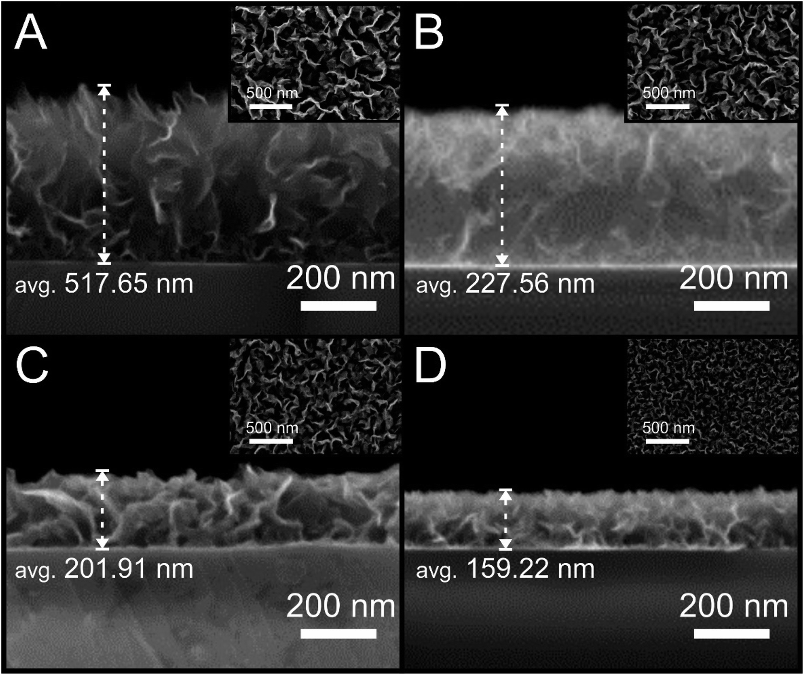
The vertically aligned graphene (VG) electrodes were fabricated via an ERC-CVD method (see Experimental section) with the distance between the plasma source and substrate varied to produce a range of VG samples with distinct microstructures (samples are supported on a SiO2/Si substrate). The distances utilised were 10, 20, 30 or 40 cm, resulting in the corresponding VG samples of V1Graphene, V2Graphene, V3Graphene and V4Graphene respectively. This approach gives rise to samples with various heights, inter-layer spacing and results in a range of edge plane densities. In order to understand the structural and compositional differences between the range of VG electrodes, Raman spectroscopy, SEM, TEM, Atomic Force Microscopy (AFM) and XPS were performed.SEM images of the VG samples are depicted in Fig. 1 (A to D respectively for V1–V4Graphene), including cross-sectional images and inserts depicting top-down views. It is clear from inspection of the SEM images that the VG samples offer an interconnected and compact network of graphene nano-flower like structural formations that are in place and extend ‘outward’ perpendicular to the substrate surface. It is also obvious to see that different spacing, heights and thus exposed edge plane densities are evident within the various graphene structures. One can determine a morphological trend based on the distance from the plasma source. As shown in Fig. 1, a decrease in the substrate–plasma distance results in an increase of the VG height, with the inverse true in the case of the largest gap/distance between the plasma and the substrate resulting in less growth, smaller graphene height and thus larger interlayer spacing. TEM characterisation (see Fig. 2) confirms this inference, illustrating the different spacing and edge plane content relating to the various exposures of the V1–V4Graphene samples.
 | ||
| Fig. 1 SEM images of V1Graphene, V2Graphene, V3Graphene and V4Graphene samples; A to D respectively. | ||
 | ||
| Fig. 2 TEM images of V1Graphene (A and B), V2Graphene (C and D), V3Graphene (E and F) and V4Graphene (G and H) respectively. | ||
Table 1 depicts the average vertical height, sheet resistivity and contact angle (CA) recorded for the VG electrodes. It is evident that the height of the VG network decreases from 517.65 nm (for V1Graphene) to 159.22 nm (for V4Graphene) as determined above, and that the recorded sheet resistivity for these samples is influenced. The sheet resistance increases from 97 to 806 Ω □−1 when comparing the V1Graphene and V4Graphene electrodes respectively. Clearly, the closer the substrate is to the plasma source the more vertical graphene growth occurs (V1Graphene), resulting in taller/bigger structures with closer stacking and more edge plane sites (a more interconnected network of layers), consequently resulting in less surface resistivity. One can potentially infer therefore that such a sample (V1Graphene) will possess favourable electrochemical properties and electrode performance compared to the inverse case (i.e. inversely V4Graphene, which at a greater plasma distance of 40 cm, has less graphene growth and larger inter-stacking distances, likely resulting in comparatively poor electrochemical responses).
| Sample | Vertical height/nm | Sheet rest., Ω □−1 | CA/degree |
|---|---|---|---|
| V1Graphene | 517.65 | 97 | 132.195 |
| V2Graphene | 227.56 | 407 | 132.988 |
| V3Graphene | 201.91 | 641 | 132.195 |
| V4Graphene | 159.22 | 806 | 133.816 |
Contact angle (CA) measurements were performed to determine the hydrophobicity of the VG samples and found to remain between 132.2 and 133.8° at the various samples, confirming the hydrophobic nature of such graphene samples,59 which is in line with literature reports on other carbon surfaces, such as on screen printed graphitic electrodes, horizontal CVD graphene and HOPG which exhibit CAs of 117, 94 and 91° respectively.60–63
Next, Raman characterisation of the graphene electrodes was performed, with the obtained spectra included in Fig. S1,† and the respective ratios, intensities and full width half-maximum (FWHM) values provided in Table S1.† The Raman spectra of the VG electrodes exhibit the typical D (ca. 1355 cm−1), G (ca. 1586 cm−1), 2D (ca. 2702 cm−1) and D + D′ (ca. 2947 cm−1) peaks, confirming the samples to indeed comprise vertical aligned graphene. Graphene's D band is well-known to relate to defects or edges in the lattice structure, the G band is generally associated to graphitic materials and the 2D band is related to the stacking order of the graphene.64,65 The I2D/IG ratios of our electrodes were 0.84, 0.81, 0.80 and 0.62 at V1–V4Graphene respectively. According to the literature,64,65 these values correspond to a flake thickness of double layer graphene for V1 and V2Graphene and few/quasi-graphene (average of 4-graphene layers) for V3 and V4Graphene respectively. The D band FWHM values from the Raman spectrum are ca. 40 to 42 cm−1, which also confirm the presence of no more than 4 (averaged) layers of graphene in all samples.64,65 FWHM values for graphene's 2D band is also a common method for estimating the number of graphene layers, where a single layer configuration exhibits a single sharp 2D band,66,67 while increasing layer numbers cause a widening of the band. The values for the 2D band's FWHM of our samples is included in Table S1† and these support the calculated number of layers reported above (although due to the nature of our vertical graphene, compared to horizontal graphene values commonly reported in the literature, we have not estimated the exact number of layers using this method). As confirmed in the SEM characterisation, vertical graphene is comprised of vertical stacks of graphene layers, which are detected via Raman as an elevated D band given that the edge plane sites are exposed.68 If requiring more information, the respective Raman fingerprints of our VG electrodes are reported in Table S1.†
XPS characterisation was performed (an overview of the acquired data is presented in Table S2†) to provide insight into the chemical composition of the VG structures, confirming the presence of two main elements: carbon (C1s at ca. 284.5 eV) and oxygen (O1s at ca. 531.7 eV). The presence of a main C1s peak at ca. 284.5 eV corresponds to C![[double bond, length as m-dash]](https://www.rsc.org/images/entities/char_e001.gif) C sp2 bonded graphitic structures, with a smaller peak at ca. 285.6 eV relating to edge plane like-sites/defects (likely C–H), and smaller peaks present at ca. 286.6 and 287 eV that are likely to correspond to adsorbed impurities (such as –C–O and –CO–/–O–CO groups). The appearance of O1s-related groups indicates that the oxygen present is bonding to the VG surface (not only adsorbed).69,70 It is important to note that the percentage of atomic O1s is 8.35, 3.30, 3.36 and 4.43% for the V1Graphene–V4Graphene samples respectively. Given these low values and the use of the near-ideal outer sphere electrochemical redox probe, RuHex, the carbon structural configuration is the only factor under investigation herein. Therefore, the electrochemical response reported is likely to vary depending only on the heights, spacing and edge plane like-sites/defects of the VG samples.
C sp2 bonded graphitic structures, with a smaller peak at ca. 285.6 eV relating to edge plane like-sites/defects (likely C–H), and smaller peaks present at ca. 286.6 and 287 eV that are likely to correspond to adsorbed impurities (such as –C–O and –CO–/–O–CO groups). The appearance of O1s-related groups indicates that the oxygen present is bonding to the VG surface (not only adsorbed).69,70 It is important to note that the percentage of atomic O1s is 8.35, 3.30, 3.36 and 4.43% for the V1Graphene–V4Graphene samples respectively. Given these low values and the use of the near-ideal outer sphere electrochemical redox probe, RuHex, the carbon structural configuration is the only factor under investigation herein. Therefore, the electrochemical response reported is likely to vary depending only on the heights, spacing and edge plane like-sites/defects of the VG samples.
Finally, AFM profiles were collected and are shown in Fig. S2,† with the corresponding data presented in Table S3† (AFM analysis includes the average roughness (Ra) and root mean square roughness (Rq), as is commonly reported in the literature). The roughness for the VG electrodes (determined by tapping-mode AFM analysis) were: Ra values of between 17.65 to 5.15 nm for the V1Graphene–V4Graphene samples respectively; and Rq values varying similarly from 23.01 to 6.67 nm (V1Graphene–V4Graphene respectively).
The physicochemical characterisation of the range of VG electrodes to be utilised for electrochemical experiments has revealed them to possess increased graphene heights and densities of layer stacking when fabricated with smaller/closer plasma–substrate distances. A decrease in the proximity of substrate and plasma source during synthesis increases the substrate temperature, which has been reported to increase the kinetics of H-radicals on the substrate surface, exhibiting higher migration energy and deposition rates of carbon and hydrocarbon clusters.71 The resultant differing resistance values and changes in the thickness of the VG networks will have a significant impact on electrochemical reactions.70
Electrochemistry at vertically aligned graphene (VG) electrodes
In order to electrochemically characterise and explore the influence of structural morphology and composition on the electrochemical performance at our various VG electrodes, the near-ideal outer-sphere redox probe hexaammineruthenium(III) chloride (RuHex, Ru(NH3)62+/3+) was employed. We utilise this well-known and widely characterised outer-sphere electrochemical redox system due to its dependence only on the electronic structure (DoS) of carbon-based electrode materials and thus the ability to relate this to the coverage of edge plane sites, which will offer useful fundamental insights. As a control and benchmarking exercise for our VG platforms, conventional (horizontal) CVD mono- and few-layer (termed quasi-) graphene and additional EPPG electrodes are studied, compared and their electrochemistry reported.Fig. 3 depicts the cyclic voltammetric signatures recorded using the RuHex electrochemical redox probe (Fig. S3† exhibits the full scan rate studies performed at the V1Graphene–V4Graphene electrodes). Table 2 reports values for the peak-to-peak separation (ΔEP), heterogeneous electron transfer (HET) rates (k0eff) and the percentage of edge plane coverage (% θedge) determined at each of the electrodes.
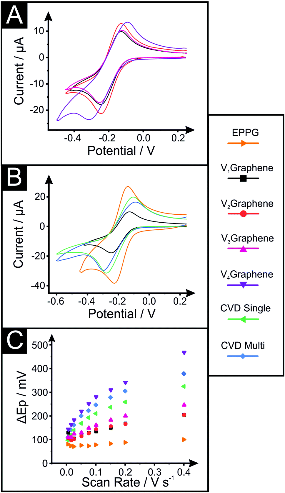 | ||
| Fig. 3 Cyclic voltammograms recorded in 1 mM RuHex in 0.1 M KCl (100 mV s−1, vs. SCE); at (A) the VG samples and (B) specifically at V1Graphene compared to CVD single-, CVD quasi-graphene and EPPG electrodes. (C) Respective plots of ΔEP against scan rate at each of the electrodes, illustrating the range of reversibility/reactivity. | ||
| ΔEP/mV (@100 mV s−1) | k 0eff/cm s−1 | % θedge | |
|---|---|---|---|
| EPPG | 100.1 | 7.60 × 10⁻³ | 1.90 |
| V1Graphene | 134.2 | 4.00 × 10⁻³ | 1.00 |
| V2Graphene | 144.1 | 2.29 × 10⁻³ | 0.57 |
| V3Graphene | 161.1 | 1.72 × 10⁻³ | 0.43 |
| V4Graphene | 280.7 | 3.05 × 10⁻⁴ | 0.08 |
| Quasi-G | 183.1 | 1.58 × 10⁻³ | 0.40 |
| Mono-G | 227.1 | 1.11 × 10⁻³ | 0.28 |
In terms of the VG samples, the ΔEP is shown to decrease as the substrate–plasma distance is shortened, indicating improved kinetics, which is evidenced and supported by the calculated HET rates (k0eff) altering from ca. 4.00 × 10⁻³ to 3.05 × 10⁻⁴ cm s−1 for V1 and V4Graphene respectively (at RuHex) – a significant change of over one order of magnitude. Correlating this to the physicochemical characterisation reported above, it is clear that the electrode possessing taller graphene structures that are stacked closer together (more dense) and thus which possesses a higher number of edge planes that are interconnected within the network of layers, not only exhibits less surface resistivity, but this translates into improved electrochemical properties, with the favourable structural configuration beneficially influencing the DoS at the given VG electrode (V1Graphene). Furthermore, note that the electrochemical behaviour of the EPPG electrode (ca. 7.60 × 10⁻³ cm s−1) is clearly the most reversible and that the horizontal monolayer graphene (ca. 1.11 × 10⁻³ cm s−1) is less favourable for fast kinetics in electrochemistry due to their respective structures, with the VG samples completing the range between these two extremes.
The percentage of edge plane like-sites/defects coverage (% θedge) comprising the various electrode surfaces is calculated from the k0eff, as shown in the Experimental section. As expected, the mono- and quasi-CVD graphene electrodes have ca. 0.28 and 0.4% of their surface covered by edge plane like-sites/defects respectively, which compares to ca. 1.00, 0.57, 0.43 and 0.08% for the V1–V4Graphenes respectively and ca. 1.90% for EPPG. These results confirm that the EPPG electrode offers the highest coverage of active edge plane like-sites/defects (as expected), however, that the VG electrodes offer a range of edge plane coverages which vary due to their morphologies (microstructural changes such as the height of the vertical graphene network, spacing between graphene petals, and network density).
To investigate the implications of the various structural configurations further and add robustness to the above observations and inferences, we next explore the electrochemical redox probe TMPD (Fig. S4† depicts the voltammetric scan rate studies). Table S4† reports the (ΔEP) and HET rates (k0eff) determined at each of the electrodes when using TMPD. It is clear that the responses observed at TMPD follow the same trend reported with RuHex. An exception to this is the response of V1Graphene, which exhibits k0eff and ΔEP values that are somewhat perturbed from the expectation and trend evident at the other electrodes. In-depth consideration of the physicochemical characterisation relating to this electrode reveals that the unusual response is likely due to the higher percentage of surface oxygen species it possesses when compared with the alternatives (i.e. ca. 8% vs. ca. 3%, see Table S2†)53,57,58 where, although reported as an outer-sphere redox probe, it has been reported previously that unusually high levels of oxygenated surface groups can inhibit the electrochemical process with TMPD;53,72 thus we have included the results for this electrode in appropriate tables/figures but will exclude V1Graphene from our discussion so that we are able to compare ‘like for like’.
With respect to the electrochemical performance of TMPD at the VG electrodes, the observed ΔEP values change from ca. 87.9 to 200.2 mV (at 100 mV s−1) as one moves from V2Graphene to V4Graphene (see Table S4†), and hence support the earlier inferences that the electrochemical response is more favourable at the taller, denser and edge plane abundant VG structure (V2Graphene in this case). Calculated HET rates (k0eff) corroborate these findings, decreasing from ca. 5.47 × 10⁻³ to 1.28 × 10⁻³ cm s−1 when determined at V2Graphene compared to V4Graphene respectively. Note that for this probe (TMPD), the ΔEP values for monolayer graphene and EPPG were ca. 205.1 and 95.2 mV (at 100 mV s−1) and calculated k0eff values were ca. 1.81 × 10⁻³ and 8.00 × 10⁻³ cm s−1 respectively. These results, as expected, allow a range to be determined where EPPG possesses the most densely stacked graphene layers (largest coverage of edge plane sites) and consequently the most favourable electrochemical kinetics, with the various VG samples completing an inner range of performances varying from fast (V2Graphene) to slow (V4Graphene) kinetics (correlating to the respective edge plane content and changing morphology/microstructure), and with monolayer horizontally aligned graphene possessing the slowest HET rates given its low edge plane composition.
Considering the full range of redox probes and samples studied herein (i.e. the horizontal mono- and quasi-graphene, the VG, and the EPPG structures/electrodes at both RuHex and TMPD) and considering the electrochemical response in relation to the physicochemical characterisation, a clear correlation is evident between the orientation, height, layer-density and interconnectivity of the graphene layers/network, such that those structures possessing a higher number of edge plane sites exhibit improved and favourable electrochemical properties. Fig. 4 depicts a visual illustration of these findings, where a trend in the relationship between the reported electrochemical properties of the VG samples (when compared to EPPG and CVD horizontal graphene) has been shown to be directly related to the structural geometry and composition of the different VG networks. We have de-convoluted the electrochemical responses and provided evidence that a higher density of edge plane like-site/defects (when using VG electrodes) results in improved HET rates. Experimental observations confirm that the vertical graphene structures reported offer intermediate platforms in terms of HET kinetics, between the two extremes of horizontal monolayer graphene (exhibiting the slowest kinetics) and that of EPPG (from HOPG) possessing the most densely stacked layers and hence the fastest HET rates and electrochemical reversibility. Regarding the performance of the VG samples (and based on the electron transfer rates recorded at the outer-sphere redox probe RuHex), we conclude that V1Graphene exhibits the largest θedge and resultantly exhibits the fastest k0eff value due to its microstructure.
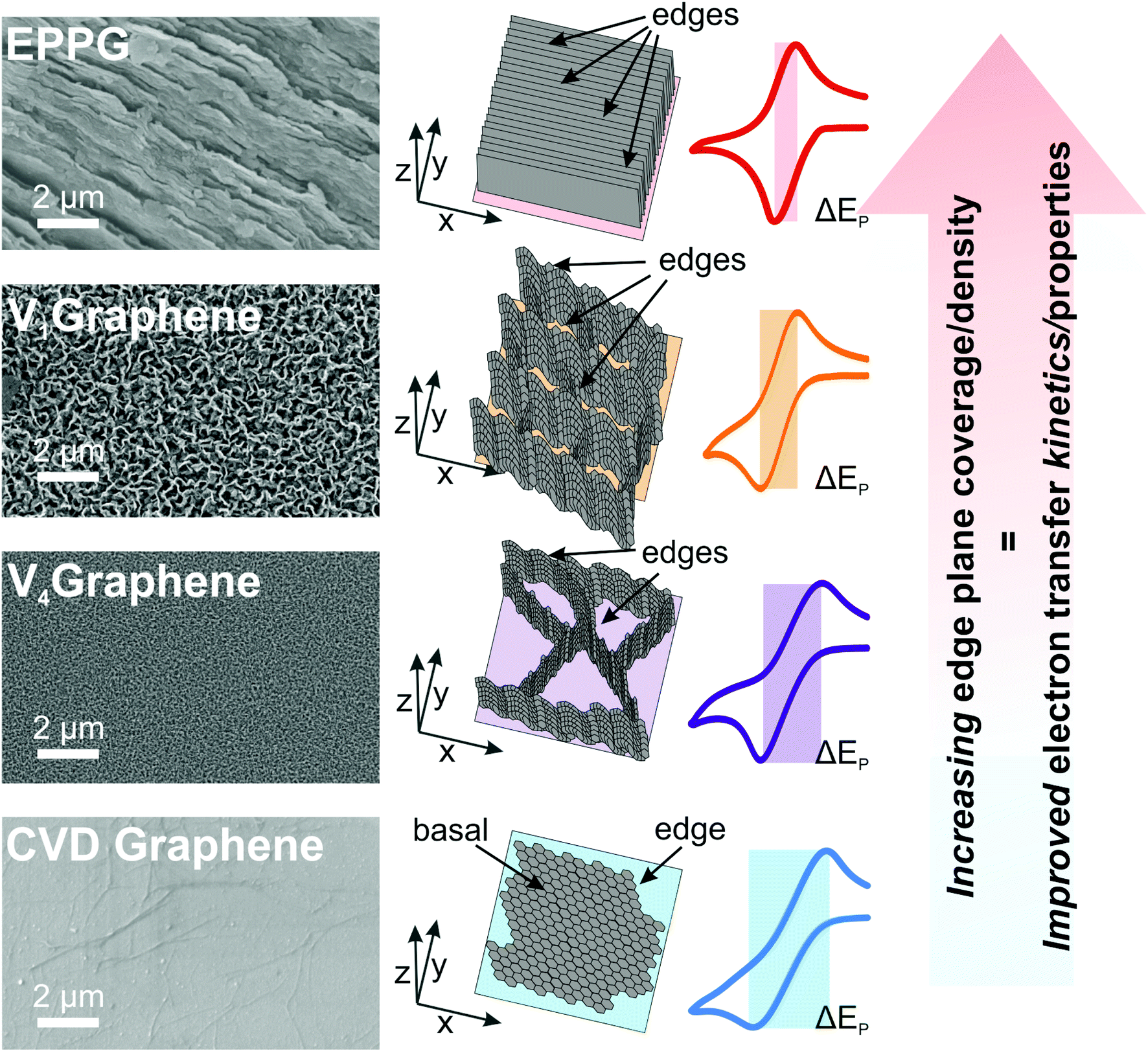 | ||
| Fig. 4 Schematic illustrating the effect of the microstructure height, spacing, edge density and inter-connected networks of VG electrodes in relation to electrochemical response. The range of structures offer a tailored/tuneable electrochemical platform in terms of HET kinetics, where CVD grown ‘flat’ graphene exhibits slow rates and the EPPG electrode possesses the fastest HET. | ||
The wide range of performances observed/reported herein with respect to a change in the structural configuration and the consequent number of available edge plane sites supports the inference that such microstructural features are the predominant origin of fast electron transfer kinetics. These are shown to influence the macroscale electrochemical response and as such, these fundamental insights (in the absence of influence from oxygenated species) will allow researchers to effectively tailor their electrode composition to attain the desired kinetic response required for specific applications in the future.
Conclusions
We have, for the first time, shown a correlation in the structure of ECR-CVD grown vertically aligned graphene (VG) directly upon its heterogeneous electron transfer (HET) kinetics in terms of the density of active edge plane like-site/defects comprising the microstructure. VGs with a larger height, close interlayer stacking, and thus an improved density of edge plane sites exhibited improved electrochemical responses compared to the inverse. Importantly, given that pristine monolayer graphene has a low degree of edge plane coverage compared to the multilayered structures of quasi-graphene and EPPG (and the favourably aligned VGs), in comparison, it exhibits poor electrochemical properties in terms of ‘fast’ HET kinetics. The ability to tailor graphene's electrochemical response through surface composition/control makes this a fascinating area of study. Through performing these comparative experiments, we have been able to confirm fundamental insights, that the macroscopic electrochemical response of graphene (and carbon-based electrodes alike) is highly dependent on the global coverage and density of edge plane sites across the VG network, the presence of which determines the electrode's electrochemical behaviour.Conflicts of interest
The authors declare no competing financial and/or non-financial interests in relation to the work described herein.Acknowledgements
D. A. C. Brownson acknowledges funding from the Ramsay Memorial Fellowships Trust. Funding from the Engineering and Physical Science Research Council (Reference: EP/N001877/1), a British Council Institutional Grant Link (No. 172726574) and Innovate UK (KTP Reference: 11606) is acknowledged.References
- K. S. Novoselov, A. K. Geim, S. V. Morozov, D. Jiang, Y. Zhang, S. V. Dubonos, I. V. Grigorieva and A. A. Firsov, Science, 2004, 306, 666–669 CrossRef CAS.
- R. L. McCreery, Chem. Rev., 2008, 108, 2646–2687 CrossRef CAS.
- J. O. Besenhard and H. P. Fritz, Angew. Chem., Int. Ed. Engl., 1983, 22, 950–975 CrossRef.
- D. A. C. Brownson, D. K. Kampouris and C. E. Banks, J. Power Sources, 2011, 196, 4873–4885 CrossRef CAS.
- D. A. C. Brownson and C. E. Banks, Analyst, 2010, 135, 2768–2778 RSC.
- M. Pumera, Chem. Rec., 2009, 9, 211–223 CrossRef CAS.
- D. A. C. Brownson, P. J. Kelly and C. E. Banks, RSC Adv., 2015, 5, 37281–37286 RSC.
- K. Zeng and D. Zhang, Prog. Energy Combust. Sci., 2010, 36, 307–326 CrossRef CAS.
- W. M. Singh, T. Baine, S. Kudo, S. Tian, X. A. N. Ma, H. Zhou, N. J. DeYonker, T. C. Pham, J. C. Bollinger, D. L. Baker, B. Yan, C. E. Webster and X. Zhao, Angew. Chem., Int. Ed., 2012, 51, 5941–5944 CrossRef CAS.
- S. Srinivasan and F. J. Salzano, Int. J. Hydrogen Energy, 1977, 2, 53–59 CrossRef.
- H. Sun, A. Varzi, V. Pellegrini, D. A. Dinh, R. Raccichini, A. E. Del Rio-Castillo, M. Prato, M. Colombo, R. Cingolani, B. Scrosati, S. Passerini and F. Bonaccorso, Solid State Commun., 2017, 251, 88–93 CrossRef CAS.
- A. J. Slate, D. A. C. Brownson, A. S. Abo Dena, G. C. Smith, K. A. Whitehead and C. E. Banks, Phys. Chem. Chem. Phys., 2018, 20, 20010–20022 RSC.
- A. García-Miranda Ferrari, H. M. Elbardisy, V. Silva, T. S. Belal, W. Talaat, H. G. Daabees, C. E. Banks and D. A. C. Brownson, Anal. Methods, 2020, 12, 2133–2142 RSC.
- D. A. C. Brownson, S. A. Varey, F. Hussain, S. J. Haigh and C. E. Banks, Nanoscale, 2014, 6, 1607–1621 RSC.
- A. T. Valota, I. A. Kinloch, K. S. Novoselov, C. Casiraghi, A. Eckmann, E. W. Hill and R. A. W. Dryfe, ACS Nano, 2011, 5, 8809–8815 CrossRef CAS.
- A. Ambrosi, C. K. Chua, A. Bonanni and M. Pumera, Chem. Rev., 2014, 114, 7150–7188 CrossRef CAS.
- A. C. Ferrari, F. Bonaccorso, V. Fal'ko, K. S. Novoselov, S. Roche, P. Bøggild, S. Borini, F. H. L. Koppens, V. Palermo, N. Pugno, J. A. Garrido, R. Sordan, A. Bianco, L. Ballerini, M. Prato, E. Lidorikis, J. Kivioja, C. Marinelli, T. Ryhänen, A. Morpurgo, J. N. Coleman, V. Nicolosi, L. Colombo, A. Fert, M. Garcia-Hernandez, A. Bachtold, G. F. Schneider, F. Guinea, C. Dekker, M. Barbone, Z. Sun, C. Galiotis, A. N. Grigorenko, G. Konstantatos, A. Kis, M. Katsnelson, L. Vandersypen, A. Loiseau, V. Morandi, D. Neumaier, E. Treossi, V. Pellegrini, M. Polini, A. Tredicucci, G. M. Williams, B. Hee Hong, J.-H. Ahn, J. Min Kim, H. Zirath, B. J. van Wees, H. van der Zant, L. Occhipinti, A. Di Matteo, I. A. Kinloch, T. Seyller, E. Quesnel, X. Feng, K. Teo, N. Rupesinghe, P. Hakonen, S. R. T. Neil, Q. Tannock, T. Löfwander and J. Kinaret, Nanoscale, 2015, 7, 4598–4810 RSC.
- D. A. C. Brownson and C. E. Banks, The Handbook of Graphene Electrochemistry, Springer-Verlag, London, 2014 Search PubMed.
- T. Tite, E. A. Chiticaru, J. S. Burns and M. Ioniţă, J. Nanobiotechnol., 2019, 17, 101 CrossRef.
- V. A. Kislenko, S. V. Pavlov and S. A. Kislenko, Electrochim. Acta, 2020, 341, 136011 CrossRef CAS.
- N. Ghaderi and M. Peressi, J. Phys. Chem. C, 2010, 114, 21625–21630 CrossRef CAS.
- R. Dettori, E. Cadelano and L. Colombo, J. Phys.: Condens. Matter, 2012, 24, 104020 CrossRef.
- P. A. Denis and F. Iribarne, J. Phys. Chem. C, 2013, 117, 19048–19055 CrossRef CAS.
- A. Shen, Y. Zou, Q. Wang, R. A. Dryfe, X. Huang, S. Dou, L. Dai and S. Wang, Angew. Chem., Int. Ed., 2014, 53, 10804–10808 CrossRef CAS.
- A. Garcia-Miranda Ferrari, C. W. Foster, D. A. C. Brownson, K. A. Whitehead and C. E. Banks, Sci. Rep., 2019, 9, 12814 CrossRef.
- S. C. S. Lai, A. N. Patel, K. McKelvey and P. R. Unwin, Angew. Chem., Int. Ed., 2012, 51, 5405–5408 CrossRef CAS.
- G. Zhang, S.-y. Tan, A. N. Patel and P. R. Unwin, Phys. Chem. Chem. Phys., 2016, 18, 32387–32395 RSC.
- L. Wang, A. Ambrosi and M. Pumera, Angew. Chem., Int. Ed., 2013, 52, 13818–13821 CrossRef CAS.
- L. C. S. Figueiredo-Filho, D. A. C. Brownson, O. Fatibello-Filho and C. E. Banks, Analyst, 2013, 138, 4436–4442 RSC.
- D. A. C. Brownson, G. C. Smith and C. E. Banks, R. Soc. Open Sci., 2017, 4, 171128 CrossRef.
- D. A. C. Brownson, J. P. Metters, D. K. Kampouris and C. E. Banks, Electroanalysis, 2011, 23, 894–899 CrossRef CAS.
- M. Pumera, ACS Catal., 2020, 10, 7087–7092 CrossRef CAS.
- C. Mattevi, H. Kim and M. Chhowalla, J. Mater. Chem., 2011, 21, 3324–3334 RSC.
- R. Muñoz and C. Gómez-Aleixandre, Chem. Vap. Deposition, 2013, 19, 297–322 CrossRef.
- X. Li, W. Cai, J. An, S. Kim, J. Nah, D. Yang, R. Piner, A. Velamakanni, I. Jung, E. Tutuc, S. K. Banerjee, L. Colombo and R. S. Ruoff, Science, 2009, 324, 1312–1314 CrossRef CAS.
- H. Xin and W. Li, Appl. Phys. Rev., 2018, 5, 031105 Search PubMed.
- E. S. Polsen, D. Q. McNerny, B. Viswanath, S. W. Pattinson and A. John Hart, Sci. Rep., 2015, 5, 10257 CrossRef.
- S. Bae, H. Kim, Y. Lee, X. Xu, J. S. Park, Y. Zheng, J. Balakrishnan, T. Lei, H. R. Kim, Y. I. Song, Y. J. Kim, K. S. Kim, B. Ozyilmaz, J. H. Ahn, B. H. Hong and S. Iijima, Nat. Nanotechnol., 2010, 5, 574–578 CrossRef CAS.
- S. Deng, D. Chao, Y. Zhong, Y. Zeng, Z. Yao, J. Zhan, Y. Wang, X. Wang, X. Lu, X. Xia and J. Tu, Energy Storage Mater., 2018, 12, 137–144 CrossRef.
- S. Zheng, M. Li, H. Li, C. Li, P. Li, L. Qian and B. Yang, J. Mater. Chem. B, 2020, 8, 298–307 RSC.
- D. Cui, H. Li, M. Li, C. Li, L. Qian, B. Zhou and B. Yang, ACS Appl. Energy Mater., 2019, 2, 1526–1536 CrossRef CAS.
- J. Scremin, I. V. Joviano dos Santos, J. P. Hughes, A. García-Miranda Ferrari, E. Valderrama, W. Zheng, X. Zhong, X. Zhao, E. J. R. Sartori, R. D. Crapnell, S. J. Rowley-Neale and C. E. Banks, Nanoscale, 2020, 12, 18214–18224 RSC.
- Z. Zhang, C.-S. Lee and W. Zhang, Adv. Energy Mater., 2017, 7, 1700678 CrossRef.
- J. R. Miller, R. A. Outlaw and B. C. Holloway, Science, 2010, 329, 1637–1639 CrossRef CAS.
- W. Li, N. Islam, G. Ren, S. Li and Z. Fan, Materials, 2019, 12, 604 CrossRef CAS.
- S. Ghosh, K. Ganesan, S. R. Polaki, S. Ilango, S. Amirthapandian, S. Dhara, M. Kamruddin and A. K. Tyagi, RSC Adv., 2015, 5, 91922–91931 RSC.
- S. Ghosh, K. Ganesan, S. R. Polaki, T. Mathews, S. Dhara, M. Kamruddin and A. K. Tyagi, Appl. Surf. Sci., 2015, 349, 576–581 CrossRef CAS.
- Graphene Supermarket, http://www.graphene-supermarket.com, accessed 10/06/2020 Search PubMed.
- A. García-Miranda Ferrari, D. A. C. Brownson and C. E. Banks, Sci. Rep., 2019, 9, 15961 CrossRef.
- D. A. C. Brownson and C. E. Banks, Phys. Chem. Chem. Phys., 2012, 14, 8264–8281 RSC.
- R. S. Nicholson, Anal. Chem., 1965, 37, 1351–1355 CrossRef CAS.
- S. J. Rowley-Neale, D. A. C. Brownson and C. E. Banks, Nanoscale, 2016, 8, 15241–15251 RSC.
- A. García-Miranda Ferrari, C. W. Foster, P. Kelly, D. A. C. Brownson and C. E. Banks, Biosensors, 2018, 8, 53 CrossRef.
- Y. Wang, J. G. Limon-Petersen and R. G. Compton, J. Electroanal. Chem., 2011, 652, 13–17 CrossRef CAS.
- A. García-Miranda Ferrari, D. A. C. Brownson, A. S. Abo Dena, C. W. Foster, S. J. Rowley-Neale and C. E. Banks, Nanoscale Adv., 2020, 2, 264–273 RSC.
- I. Lavagnini, R. Antiochia and F. Magno, Electroanalysis, 2004, 16, 505–506 CrossRef CAS.
- R. G. Compton and C. E. Banks, Understanding Voltammetry, Imperial College Press, 2nd edn, 2010 Search PubMed.
- R. C. Alkire, P. N. Barlett and J. Lipkowski, Electrochemistry of Carbon Electrodes, Wiley, 2016 Search PubMed.
- S. Tian, L. Li, W. Sun, X. Xia, D. Han, J. Li and C. Gu, Sci. Rep., 2012, 2, 511 CrossRef.
- S. Wang, Y. Zhang, N. Abidi and L. Cabrales, Langmuir, 2009, 25, 11078–11081 CrossRef CAS.
- Y. J. Shin, Y. Wang, H. Huang, G. Kalon, A. T. S. Wee, Z. Shen, C. S. Bhatia and H. Yang, Langmuir, 2010, 26, 3798–3802 CrossRef CAS.
- B. N. Chandrashekar, B. Deng, A. S. Smitha, Y. Chen, C. Tan, H. Zhang, H. Peng and Z. Liu, Adv. Mater., 2015, 27, 5210–5216 CrossRef CAS.
- G. Ibáñez-Redín, D. Wilson, D. Gonçalves and O. N. Oliveira, J. Colloid Interface Sci., 2018, 515, 101–108 CrossRef.
- A. C. Ferrari, Solid State Commun., 2007, 143, 47–57 CrossRef CAS.
- D. Graf, F. Molitor, K. Ensslin, C. Stampfer, A. Jungen, C. Hierold and L. Wirtz, Nano Lett., 2007, 7, 238–242 CrossRef CAS.
- A. C. Ferrari, J. C. Meyer, V. Scardaci, C. Casiraghi, M. Lazzeri, F. Mauri, S. Piscanec, D. Jiang, K. S. Novoselov, S. Roth and A. K. Geim, Phys. Rev. Lett., 2006, 97, 187401 CrossRef CAS.
- Y. Y. Wang, Z. H. Ni, Z. X. Shen, H. M. Wang and Y. H. Wu, Appl. Phys. Lett., 2008, 92, 043121 CrossRef.
- S. Ghosh, K. Ganesan, S. R. Polaki, T. R. Ravindran, N. G. Krishna, M. Kamruddin and A. K. Tyagi, J. Raman Spectrosc., 2014, 45, 642–649 CrossRef CAS.
- T. Uchida, A. Baliyan, T. Fukuda, Y. Nakajima and Y. Yoshida, RSC Adv., 2014, 4, 36071–36078 RSC.
- P. Ji, J. Chen, T. Huang, C. Jin, L. Zhuge and X. Wu, Diamond Relat. Mater., 2020, 108, 107958 CrossRef CAS.
- L. Cui, J. Chen, B. Yang, D. Sun and T. Jiao, Appl. Surf. Sci., 2015, 357, 1–7 CrossRef CAS.
- D. A. C. Brownson, G. Smith and C. E. Banks, R. Soc. Open Sci., 2017, 4, 171128 CrossRef.
Footnote |
| † Electronic supplementary information (ESI) available. See DOI: 10.1039/d0na00587h |
| This journal is © The Royal Society of Chemistry 2020 |