DOI:
10.1039/D0NA00503G
(Paper)
Nanoscale Adv., 2020,
2, 4566-4580
Strain-induced band modulation and excellent stability, transport and optical properties of penta-MP2 (M = Ni, Pd, and Pt) monolayers†
Received
19th June 2020
, Accepted 30th August 2020
First published on 31st August 2020
Abstract
First principle calculations utilizing density functional theory were carried out to investigate the electronic, transport and optical properties of penta-MP2 (M = Ni, Pd and Pt) monolayer compounds under applied uniaxial and biaxial tensile strains. With an optimum magnitude of applied strain, we found band gap transitions in penta-MP2 monolayers from zero/narrow to the semiconductor regime, wherein band gaps were noticed to be firmly dependent on the applied uniaxial and biaxial tensile strains. In this study, the PBE approach was used primarily to evaluate electronic properties, from where the identified architectures of penta-MP2 with maximum obtained bandgaps under respective optimum strains were assessed through the HSE06 method of calculation for better estimation of band gaps and optical properties. Prior to HSE calculations, we affirmed our assessment for the stability and reliability of the compounds under uniaxial and biaxial strains of up to 15% through phonon spectrum and elastic calculations. A distinct transition was also noted from semiconductor to metal for all compounds after the applied optimum uniaxial and biaxial strains. The optical absorption spectra in all the stretched penta-MP2 compounds reached the order of 106 cm−1, with significant peaks belonging to the IR and visible regions; this indicates promising applications of these materials in high-performance solar energy and good hot mirror materials. The enhanced I–V responses under uniaxial and biaxial tensile strains using the non-equilibrium Green's function (NEGF) approach confirm the usefulness of the strained state of the considered penta-MP2 monolayers. The results show that tuning electronic properties, I–V characteristics and optical properties of stretched penta-MP2 compounds under tensile strain merits significant future applications in optoelectronic devices and as good hot mirror materials.
Introduction
The discovery of graphene in 2004 (ref. 1–3) encouraged substantial scientific efforts in the research community to explore two-dimensional (2D) materials, as they exhibit outstanding physical, mechanical, electronic, optical and transport properties. Various technical developments have contributed to the ongoing explosion in the development of these materials, and various innovative 2D technologies have been introduced.4–7 In addition, numerous modern 2D nanostructures have been theoretically proposed with the aid of high-performance computing,8–11 and a few of these predicted 2D compounds were successfully fabricated through experiments. Two-dimensional B (boron) and Si (silicene) are among the best examples in this regard.12–14 Due to the zero band-gap of graphene, much attention has been paid to investigating 2D semiconductor materials such as phosphorene15,16 and transition-metal dichalcogenides.17,18 In the recent past, 2D materials with pentagon shapes have also been reported, with fascinating properties. In 2015, penta-graphene was reported by Zhang et al.;19 it is formed by the strong sp2/sp3 hybridization of carbon atoms along with high mechanical and dynamical stability up to 1000 K, through AIMD simulations.19 Numerous efforts have been made by many researchers to invent 2D materials with penta structures since the successful prediction of penta-graphene.20,21 Moreover, 2D group V phosphorene has been successfully separated from bulk black phosphorus;22 its bandgap was measured to be about ∼2.0 eV, and possesses a high carrier mobility of up to 104 cm2 V1 s1.8 However, due to the issue of rapid degradability in black phosphorus, developed 2D phosphorene derivatives, including GeP3,23 InP3,24 δ-InP3,25 SnP3,26,27 and CaP3,28 have been paid immense attention due to expectations of high carrier mobility. Experimentally, a pentagon-shaped PdSe2 compound with puckered geometry was successfully exfoliated from its bulk crystal with a bandgap of 1.3 eV and good carrier mobility of ∼158 cm2 V1 s1,29 whereas GeP2 also showed outstanding results in photocatalysis of the splitting of CO2 into CO and of water splitting.30 In addition to this work, many other studies have been reported on metallic 2D pentagon-based materials such as penta-graphene,19 penta-silicene,31 penta-SiN32 and penta-CN;21 however, it is still exceptionally challenging to achieve wide bandgaps in pentagonal 2D semiconductors. However, it is intriguing to encourage investigation of the potential applications of 2D pentagon-based wide bandgap phosphide materials. Hence, more efforts to explore the potential of pentagon-based compounds may be worthwhile for future useful applications. Qian et al.33,34 and Yuan H. et al.33,34 introduced new binary penta transition-metal phosphide/arsenide compounds, MX2 (M = Ni, Pd and Pt; X = P and As), which have high carrier mobility with strong optical absorption spectra.33,34 The bulk phases of MX2-type materials were previously investigated in the 1960s, in which NiP2 and PdP2 crystals were found to possess monoclinic symmetry with the space group C2/c, whereas PtP2, NiAs2, PdAs2 and PtAs2 are known to possess cubic symmetry.35 Studies of these compounds at the DFT-PBE level show a significantly lower band gap (∼0–0.1 eV), which essentially restricts researchers from studying them further in applicable scientific fields. In order to overcome this lower bandgap issue, researchers are continuously engaged in the quest to increase the bandgaps of these materials under various external stimuli for possible applications. Bandgap engineering has been explored through applied external electric field, strain, doping, etc.; this has been shown to be a feasible way to control the bandgap, as required for commonly useful low-dimensional systems.36–40 The practical use of any two-dimensional material for design and manufacturing generally depends on a better understanding of its strength and mechanical behavior.41,42 The optimum strength is the maximum stress under which a perfect crystal can survive at zero temperature while analyze the strength and complete stability of its chemical bonds.43,44 In addition, strain can be utilized to tune the bandgap of most 2D compounds. Thus, the elastic limit must be determined to understand how structures differ with stress. In the past, work on blue phosphorene, β-arsenene and β-antimonene has shown that these materials have flexible bandgaps and are strongly dependent on the number of layers, modulated by applied directional strain.45–49 It can be understood from the above discussion that tensile strain can be an excellent technique to tune the energy bandgaps of 2D materials and to endow them with useful properties in a versatile range of nanoelectronic and optoelectronic applications.
In the present work, we have performed a systematic investigation of the electronic properties of a series of monolayer penta-MP2 (M = Ni, Pd and Pt) compounds under tensile strains of up to 15% using density functional theory (DFT).50 Initially, we considered the Perdew–Burke–Ernzerhof (PBE)51,52 approach for bandgap modulation to find the maximum bandgap value with respect to a particular amount of strain in the uniaxial and biaxial directions. The enhanced bandgap achieved for a particular amount of strain confirmed the possible existence of the compound in reality under the influence of external strains in the uniaxial and biaxial directions through phonon and mechanical stabilities. Because PBE calculations are known to underestimate bandgap values, we further carried out the popular Heyd–Scuseria–Ernzerhof (HSE06)53,54 hybrid calculations to better estimate the bandgap values. The optical properties of the considered materials were also explored with HSE06 calculations. In addition, the current–voltage (I–V) characteristics of the penta-MP2 compounds exhibit isotropic transport properties with and without strain. The present theoretical investigation reveals the bandgap modulation of penta-MP2 compounds with remarkably enhanced optical absorption spectra (order of 106 cm−1) in the infra-red (IR) and visible ranges of the electromagnetic spectrum, which provides a new direction for their applications in the fields of nanoelectronics and optoelectronics.
Computational details
The ground state structures and electronic properties of penta-MP2 (M = Ni, Pd and Pt) were calculated using density functional theory (DFT)50 under the generalized gradient approximation (GGA), as implemented in the Vienna ab initio Simulation Package (VASP)55–58 with the Perdew–Burke–Ernzerhof (PBE)51,52 functional as the exchange–correlation interactions.58,59 To understand the electron–ion interactions, we used projector-augmented wave pseudopotentials (PAW).59,60 All the calculations were carried out with a plane wave energy cutoff of 550 eV, employed with the Monkhorst–Pack 15 × 15 × 1 Γ-centre k-mesh as used for Brillouin zone integrations. The minimum optimization criteria were considered until the total energy convergence reached 10−7 eV per atom. Both the ionic position and unit cell were optimized by considering the criteria for maximum residual forces on each atom reaching less than 0.001 eV Å−1 under the conjugate gradient method. For geometry optimization and accurate energy band calculations, Fermi-level smearing was taken as 0.01 eV. To avoid interactions between two adjacent layers, we preserved a minimum of ∼20 Å of vacuum space. It is well known that PBE-DFT usually underestimates electronic band gaps. To overcome this issue, we also employed a very popular hybrid functional, Heyd–Scuseria–Ernzerhof (HSE06),53,54 to obtain more accurate band gap values. The mixing parameter of the HSE06 functional used in the present work was 25% Hartree–Fock (HF) exchange with 75% PBE exchange, which has been reported to achieve the best possible matches to experimental band gap values in the past:53,54,61,62| |  | (1) |
Employing density functional perturbation theory (DFPT)63 interfaced with phonopy64 code, we evaluated the dynamical strength using the small displacement method of atoms with 4 × 4 × 1 supercells for all the considered structures, and the phonon spectra were determined using the obtained second order force constant. The VESTA65 tool was used for visualization and construction of the structures of the materials. In addition, we also investigated the electronic transport properties with the non-equilibrium Green's function (NEGF) methods using Landauer–Buttiker equations as follows:66,67
| |  | (2) |
where
G0 is the unit of the quantum conductance,
T(
E,
Vb) is the transmission probability of incident electrons at a potential bias
Vb and energy
E, and
μL and
μR are the electrochemical potentials of the left and right electrodes at a particular voltage bias difference with
eVb =
μL −
μR. The probability of transmission of electrons from left to right with the given energy
E was calculated as follows:
68| | | T(E,V) = Tr[αR(E,V)GR(E,V)αL(E,V)GL(E,V)GA(E,V)] | (3) |
where
α and
GA denote the coupling matrix of the electrodes and the Green's function of the central region, respectively.
Results and discussion
Structural properties
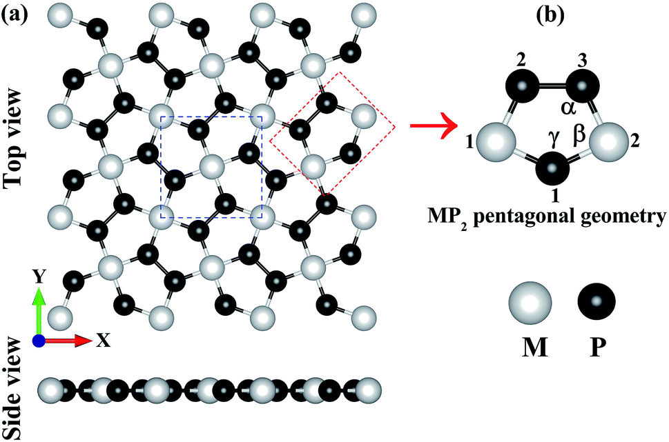
In Fig. 1, we have shown the structure of the two-dimensional penta-MP2 (M = Ni, Pd and Pt) planar monolayer, which has a tetragonal lattice symmetry with pentagonal geometry. In the unit cell as shown in Fig. 1(a) (marked with blue dots), one Ni atom is bonded to four neighboring P atoms, and each P atom is also bonded with another P atom to increase the periodic dimension of the crystal structure. In Table 1, we provide the obtained bond angles and optimized lattice constants for NiP2, PdP2 and PtP2. The lattice constants for NiP2, PdP2 and PtP2 were obtained as 5.57 Å, 5.86 Å and 5.84 Å, respectively, which are consistent with earlier literature reports.34 The atoms of penta-MP2 were chemically exfoliated from bulk materials, as shown in the blue dotted square box. The red dotted box denotes the pentagonal symmetry of the crystal structure, in which two M atoms are linked with the three P atoms, and all P atoms are in dimers and form P–P bonds. These monolayers can be fabricated from van der Waals crystals as well as from the bulk compounds.69 According to Novoselov et al.,1 mechanical exfoliation is considered to be a suitable technique to obtain graphene monolayer nanosheets from the van der Waals coupled layered bulk graphite structure. A similar chemical exfoliation technique was adopted for chemically bonded bulk phases, such as transition metal nitrides/carbides, known as MXene compounds, to extract their monolayers.70 These findings are in line with previous reports, which suggest that the geometry of the MP2 monolayer in our present study is reliable. The penta-MP2 compounds have been reported to be stable in terms of their dynamical and mechanical aspects.34
 |
| | Fig. 1 (a) Unit cell of the 2D penta-MP2 (M = Ni, Pd and Pt) structure with top and side views, and (b) schematic of the pentagonal geometry of penta-MP2. | |
Table 1 The calculated lattice constants (a), bond lengths (Å) and bond angles (θ) of the penta-MP2 (M = Ni, Pd, and Pt) compounds
| Compound |
a (Å) |
Bond length (Å) |
Angle (θ) |
| P1–M1 |
P2–P3 |
M1–P1–M2 (α) |
P1–M2–P3 (β) |
M2–P3–P2 (γ) |
| NiP2 |
5.57 |
2.18 |
2.10 |
129.96 |
90.00 |
115.07 |
| PdP2 |
5.86 |
2.32 |
2.06 |
126.65 |
90.00 |
116.67 |
| PtP2 |
5.84 |
2.31 |
2.08 |
127.12 |
90.00 |
116.44 |
Electronic properties
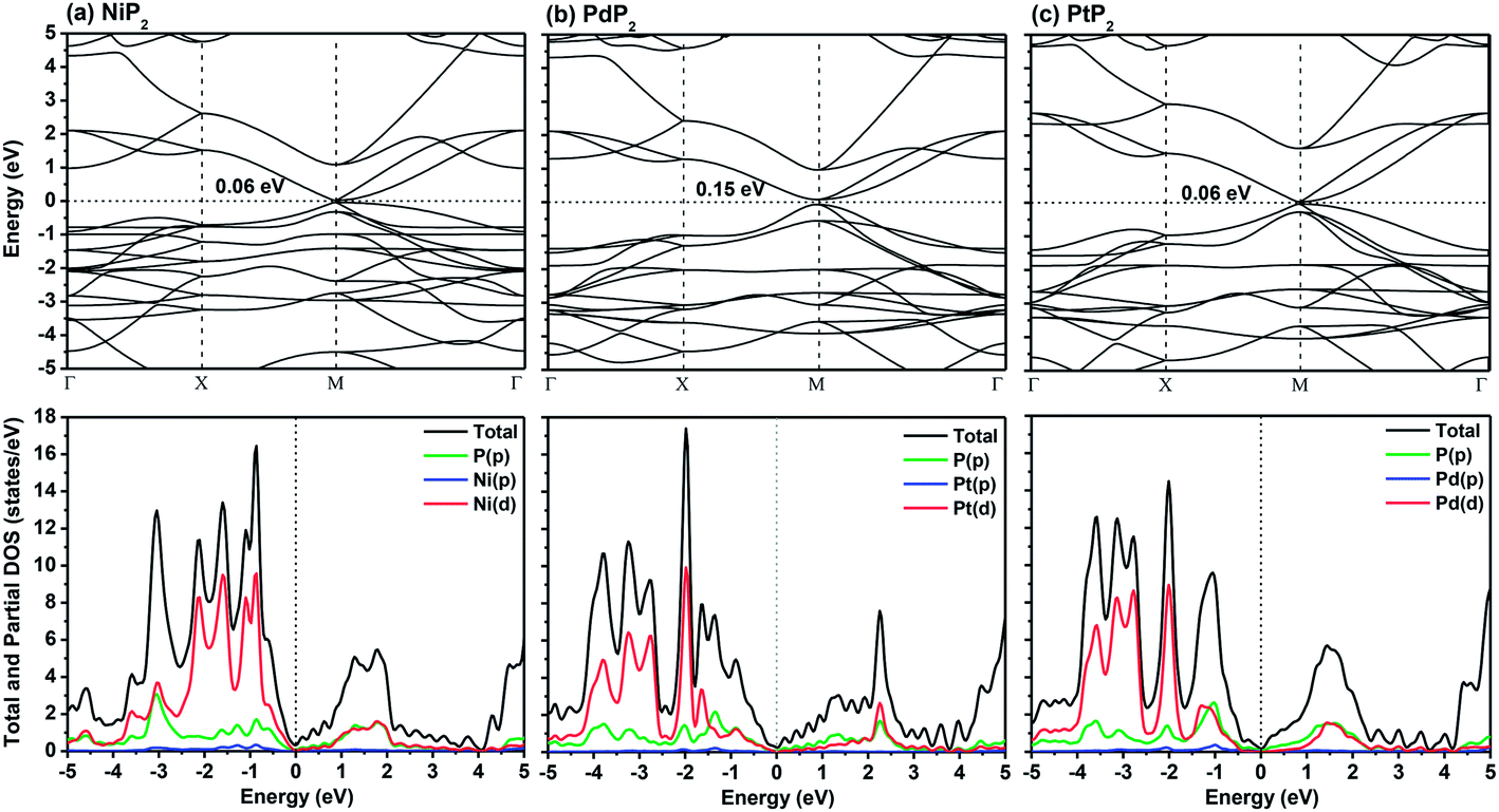
In Fig. 2, we present the electronic band structures and partial density of states diagrams of the penta-MP2 structures, which reveal very narrow direct bandgaps at the M-points of 60 meV, 150 meV and 60 meV for NiP2, PdP2 and PtP2, respectively.34 The PDOS analysis shows that the d-orbitals of the transition elements (Ni, Pd and Pt) are making the main contribution near the Fermi level in the valance band maxima (VBM), while the p and d-orbitals show major effects near the Fermi level on the conduction band maxima (CBM). It may be noted here that the narrow bandgaps of penta-MP2 create a restriction for their application in the fields of nanoelectronics and optoelectronics. In order to overcome these issues, we applied tensile strains along the uniaxial and biaxial directions of up to 15%. The magnitude of strain was calculated as S (%) = [(|a − a0|)/a0] × 100, where a0 and a are the lattice parameters of the unstrained and strained systems, respectively. Table 2 provides the optimized geometry parameters of the considered penta-MP2 compounds for a particular value of the applied uniaxial and biaxial tensile strains at which the bandgap reaches the highest value. The atom–atom bond lengths of M–P and P–P increase from their equivalent positions due to the stretching in the structure, which is responsible for the lower overlap of the electronic orbitals with those of the adjacent atoms. The variation in bandgap values with respect to the applied strains is presented in Fig. 3, where the dotted and solid lines denote the tensile strains along the uniaxial and biaxial directions, respectively.
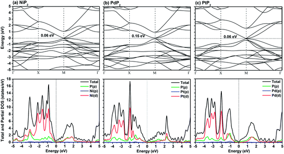 |
| | Fig. 2 The band structures and partial density of states (PDOS) diagrams of the 2D penta-MP2 (M = Ni, Pd, and Pt) compounds (a) NiP2, (b) PdP2, and (c) PtP2. | |
Table 2 Calculated bandgaps (Eg), bond lengths (Å) and bond angles (θ) of the 2D penta-MP2 (M = Ni, Pd and Pt) compounds at the respective optimum uniaxial and biaxial tensile strains
| Compound |
NiP2 |
PdP2 |
PtP2 |
| Uniaxial (12%) |
Biaxial (06%) |
Uniaxial (09%) |
Biaxial (06%) |
Uniaxial (12%) |
Biaxial (09%) |
|
E
g (eV) |
PBE |
0.35 |
0.37 |
0.26 |
0.35 |
0.44 |
0.60 |
| HSE06 |
0.86 |
1.30 |
0.80 |
0.90 |
1.02 |
1.20 |
| Bond lengths (Å) |
P1–M1 |
2.23 |
2.32 |
2.37 |
2.48 |
2.36 |
2.54 |
| P1–M2 |
2.42 |
— |
2.51 |
— |
2.57 |
— |
| P2–P3 |
2.12 |
2.13 |
2.09 |
2.10 |
2.13 |
2.16 |
| P2–M1 |
2.42 |
— |
2.51 |
— |
2.57 |
— |
| P3–M2 |
2.23 |
— |
2.37 |
— |
2.36 |
— |
| Bond angles (θ) |
M1–P1–M2 (α) |
127.83 |
— |
125.34 |
— |
125.78 |
— |
| P1–M2–P3 (β) |
94.19 |
90.00 |
93.30 |
90.00 |
93.98 |
90.00 |
| M2–P3–P2 (γ) |
110.18 |
116.01 |
112.09 |
117.52 |
111.37 |
117.47 |
| P1–M1–P2 (β′) |
85.80 |
— |
86.70 |
— |
86.01 |
— |
| M1–P2–P3 (γ′) |
121.98 |
— |
122.57 |
— |
112.84 |
— |
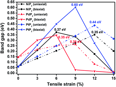 |
| | Fig. 3 The band gap variations under applied uniaxial and biaxial tensile strains for the 2D penta-MP2 (M = Ni, Pd, and Pt) compounds. | |
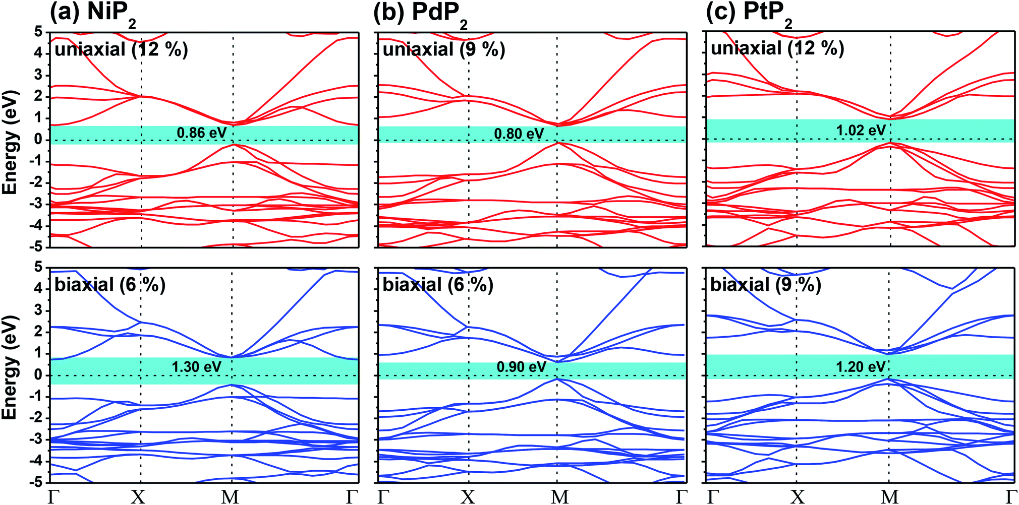
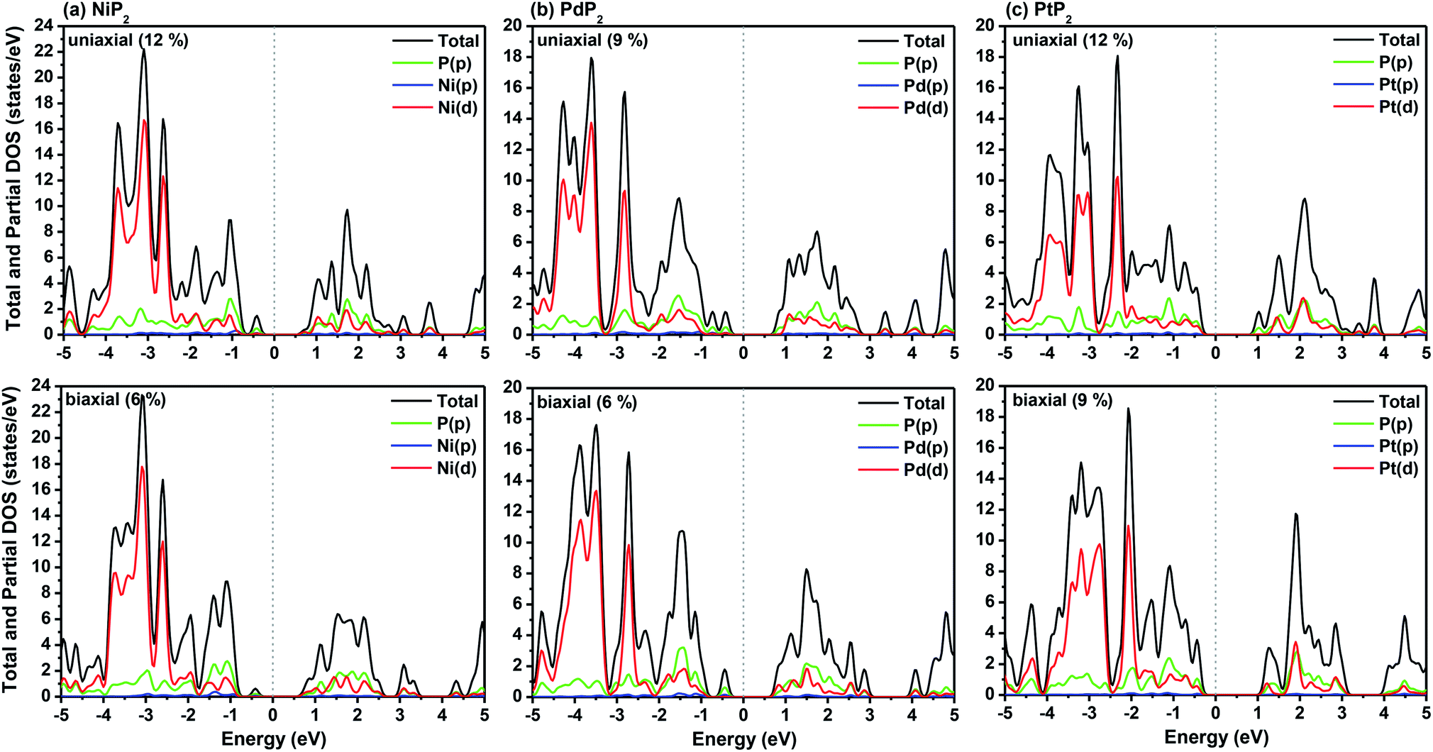
The highest PBE calculated bandgaps for the NiP2 compound were found to be 0.35 eV and 0.37 eV after applied tensile strains of 12% (uniaxial) and 6% (biaxial), respectively. For the PdP2 case, the PBE bandgap showed the maximum band gap value of 0.26 eV and 0.35 eV at tensile strains of 9% (uniaxial) and 6% (biaxial), respectively. Maximum bandgaps of 0.44 eV and 0.60 eV were observed for PtP2 for the applied strains of 12% (uniaxial) and 9% (biaxial), respectively. It was observed that the biaxial tensile strain functions more effectively than the uniaxial strain to reach the maximum bandgap with a lower applied strain effect. Moreover, if the amount of tensile strain increased beyond the critical value of the strain, the bandgap showed a decreasing nature in both cases (biaxial and uniaxial) and achieved the metallic state. The VBM and CBM of the achieved maximum bandgaps were found to be at the same M-points in the Brillouin zone, which reveals that all the penta-MP2 materials can retain their direct bandgap natures under the applied tensile strains. However, after the transitions of the PdP2 and PtP2 compounds from semiconductors to semimetals, their VBM and CBM shifted between the M and Γ k-points. The bandgap variations under applied strains of up to 15% can be understood through the band diagrams of the penta-MP2 structures, as shown in Fig. S1–S3 (ESI†). It is currently well known that PBE generally underestimates the values of bandgaps, which do not match experimental results on many occasions. In order to achieve a better estimation of the energy bandgaps, we carried out extensive calculations with the HSE06 functional only for the cases of the maximum bandgaps obtained at particular amounts of tensile strain in the PBE calculations for all the considered penta-MP2 compounds. Fig. 4 illustrates the HSE06 band diagrams of the penta-MP2 compounds under optimum uniaxial and biaxial tensile strains. The enhanced values of the bandgaps using the HSE calculations were found to be 0.86 eV (1.30 eV), 0.80 eV (0.90 eV) and 1.02 eV (1.20 eV) under uniaxial (biaxial) strains for NiP2, PdP2 and PtP2, respectively, at the M-point for all cases. Fig. 5 shows the partial density of states (PDOS) and total density of states (TDOS), wherein the above bandgaps are reflected clearly at the Fermi level. Due to the presence of d-block elements in the penta-MP2 compounds, highly intense TDOS peaks were observed. The p-orbitals of the P atoms and d-orbitals of the M (Ni, Pd and Pt) atoms show more contributions in the VBM region compared to the CBM region; meanwhile, up to −2 eV, the P(p) orbital shows a dominant nature in the VBM region near the Fermi level, and the Ni(d) orbital was found to be effective after −2 eV.
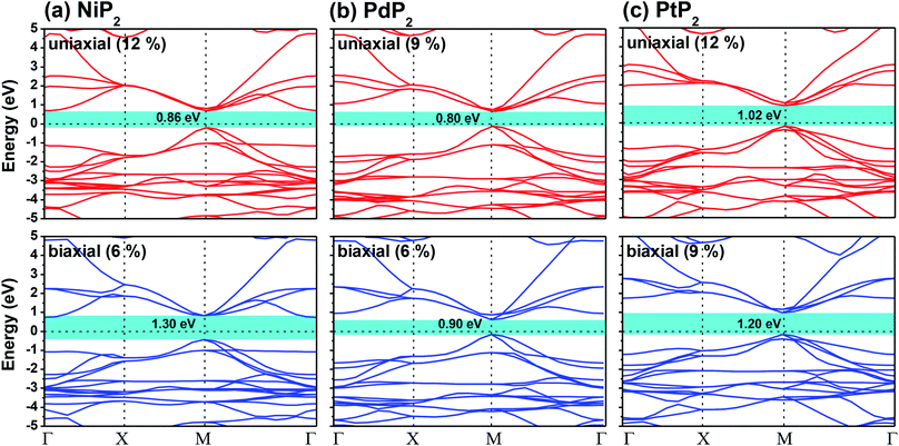 |
| | Fig. 4 HSE06 functional-calculated band diagrams at the respective optimum uniaxial and biaxial tensile strains for the penta-MP2 (M = Ni, Pd, and Pt) compounds (a) NiP2, (b) PdP2, and (c) PtP2. | |
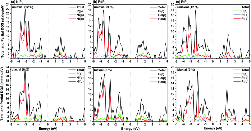 |
| | Fig. 5 HSE06 functional-calculated partial and total DOS at the respective optimum uniaxial and biaxial tensile strains for the penta-MP2 (M = Ni, Pd, and Pt) compounds (a) NiP2, (b) PdP2, and (c) PtP2. | |
In order to check the effects of dipole correction on the electronic properties of our considered systems, we calculated the effects of dipole correction on the total energy (E), work function (ф) and bandgap (Eg) for all the penta-MP2 (M = Ni, Pd and Pt) monolayers under unstrained, uniaxial and biaxial strains, as presented in Table S1 (ESI†). It can be noted from Table S1† that no notable deviations were observed in the total energy (E), work function (ф), and bandgap (Eg) due to dipole correction for our considered systems.
Stability of penta-MP2 compounds under tensile strains
It is expected that any external physical force will change the properties of a system, which may be effective to endow it with useful properties for different applications. However, it is not necessary for a system to always possess the capacity to tolerate external forces. In the present work, we also examined the application of external force to the equilibrium geometry of the penta-MP2 systems, wherein significant energy bandgaps were observed. Therefore, it was also essential for us to investigate the possible stability of the penta-MP2 systems under applied tensile strains. Therefore, in order to determine the stability of the penta-MP2 monolayers, we obtained the frequency-dependent phonon dispersion curves along the high symmetry paths in the Brillouin region (Fig. S4–S6, ESI†). It is heartening to note that under the tensile strains applied to the penta-MP2 structures, no negative frequency was found under the uniaxial and biaxial strains up to of 12% and 9%, respectively, which essentially confirms the stable states for all the maximum bandgaps obtained under the respective uniaxial and biaxial strains. It was noted that in the Γ-points, the low-frequency optical and acoustic modes appeared to be well separated from each other. We also observed a continuous decrease of frequency with increasing magnitude of both the uniaxial and biaxial strains, which is also responsible for the lower thermal conductivity. In Fig. S4–S6 (ESI†), the black-marked phonon diagrams illustrate the maximum bandgaps achieved at the optimum applied strains. Overall, the absence of negative frequency under the optimum tensile strains strongly indicates the dynamical stability of our considered penta-MP2 (M = Ni, Pd and Pt) compounds.
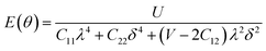
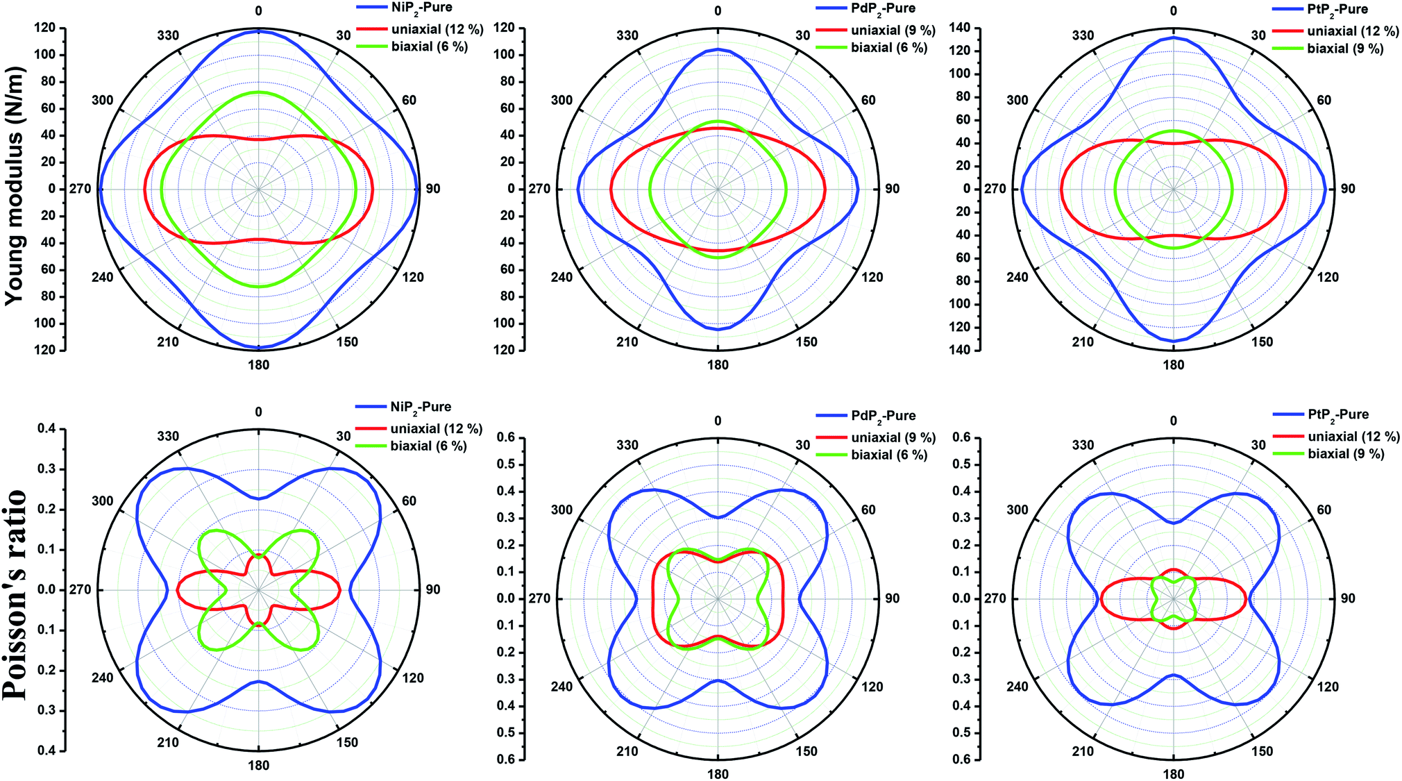
Furthermore, we carried out an investigation on the mechanical stability of the considered penta-MP2 systems under the optimum tensile strains for which the maximum bandgaps were obtained. The linear elastic constants of the penta-MP2 systems were obtained by the finite distortion method.19 The Voigt notations (1-xx, 2-yy, and 6-xy)71 for biaxial strain-dependent elastic constants have three independent terms of C11, C12 and C66, which denote isotropic nature by having the same symmetry for C11 and C22, while the uniaxial strain-dependent elastic constants have four independent terms, including C22, in which C11 ≠ C22, which represents anisotropic nature. The in-plane axial Young's moduli and Poisson's ratios for our systems were calculated by the equations Ex = (C112 − C122)/C11; Ey = (C122 − C122)/C22; and νx = C12/C11; νx = C12/C22, respectively, and the results are tabulated in Table 3. Because the present materials possess three-dimensional (3D) periodic limits, their two-dimensional elastic constants (Cij) were rescaled by multiplying the c factor of the lattice parameter corresponding to the vacuum space between the two conjugative 2D layers,71–73i.e., C2Dij = c × C3Dij. It should be noted that a mechanically stable 2D structure must fulfill the Born criteria, as72 (C11C22 − C122) > 0 and C66 > 0. All the considered penta-MP2 compounds were found to be mechanically stable even under applied uniaxial and biaxial strains. The obtained Young's moduli under the strains are remarkably lower than those in the unstrained systems. For NiP2, the Young's moduli were found to be 37.78 N m−1 (uniaxial) and 72.98 N m−1 (biaxial), which are almost 3 and 1.5 times lower than those of the unstrained system. Also, in the cases of PdP2 and PtP2, the Young's moduli were found to be 2 and 3 times lower in both directions (x and xy), respectively, compared to their unstrained states. Although the Poisson's ratio (ν) slightly differs for all the penta-MP2 compounds under uniaxial strain, it is significantly reduced in the case of biaxial strain with respect to the unstrained system. In order to understand and analyze the mechanical properties of the penta-MP2, we also obtained polar diagrams of the Young's moduli E(θ) and Poisson's ratio ν(θ) using the elastic constant (Cij) as shows in the following equations:74,75
| |  | (4) |
| | 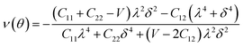 | (5) |
where
λ and
δ denote sin(
θ) and cos(
θ), respectively, and
U =
C11C22 −
C122;
V =
U/
C66. As illustrated in
Fig. 6, the unstrained and applied-biaxial-strained penta-MP
2 compounds exhibit isotropic features, while anisotropic features are observed in the case of applied uniaxial strain. It should also be noted from
Fig. 6 that the penta-MP
2 compounds appear to be stiffer under applied tensile strains than the unstrained systems owing to their larger
E(
θ). In the case of biaxial strain, all the penta-MP
2 compounds showed the highest values of
E(
θ) for the angles of 0°, 90°, 180° and 360°, similar to the unstrained case; however, because they possess anisotropic features due to the uniaxial strain, the maximum value of
E(
θ) lies in the
x-direction with angles of 90° and 270° while the minimum value lies in the
y-direction with angles of 0° and 180° for the NiP
2 and PtP
2 compounds, respectively. Similarly, the maximum
ν(
θ) for penta-MP
2 is found along the directions of 0°, 90°, 180° and 360° for both no strain and biaxial strain. The maximum
ν(
θ) under uniaxial strain lies in the
x (
y)-direction of 90° (0°) and 270° (180°) for the NiP
2 and PtP
2 compounds, respectively; meanwhile, it was found to be maximum for PdP
2 along the angles of 60° and 240° in the
x-direction and minimum along the angles of 0° and 180° in the
y-direction. Overall, the elastic constants of the penta-MP
2 compounds under the applied tensile strains indicate their reasonably good elastic properties.
Table 3 The calculated elastic constants (Cij), in-plane Young's moduli (E) in units of N m−1, and Poisson's ratios (ν) at the optimum applied uniaxial and biaxial tensile strains respective to the maximum bandgaps
| Structure |
Strain |
C11 |
C22 |
C12 |
C66 |
E
|
ν
|
| NiP2 |
Unstrained |
124.20 |
— |
28.10 |
39.30 |
117.90 |
0.23 |
| Uniaxial (12%) |
37.78 |
86.44 |
7.63 |
30.27 |
36.24(x), 85.77(y) |
0.20(x), 0.08(y) |
| Biaxial (06%) |
72.98 |
— |
5.87 |
28.36 |
72.50 |
0.08 |
| PdP2 |
Unstrained |
114.90 |
— |
34.80 |
28.40 |
104.40 |
0.28 |
| Uniaxial (09%) |
47.18 |
82.56 |
11.40 |
24.89 |
42.42(x), 80.98(y) |
0.24(x), 0.14(y) |
| Biaxial (06%) |
51.93 |
— |
7.65 |
20.70 |
50.81 |
0.15 |
| PtP2 |
Unstrained |
142.30 |
— |
40.40 |
35.90 |
131.90 |
0.25 |
| Uniaxial (12%) |
41.12 |
100.64 |
11.09 |
31.90 |
38.12(x), 99.43(y) |
0.27(x), 0.11(y) |
| Biaxial (09%) |
51.12 |
— |
3.21 |
23.29 |
50.91 |
0.06 |
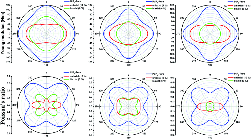 |
| | Fig. 6 Polar diagrams of the Young's moduli and Poisson's ratios under uniaxial and biaxial tensile strains for the 2D penta-MP2 (M = Ni, Pd and Pt) compounds. | |
Thermal stability of penta-MP2 under optimum strains
Ab initio molecular dynamics (AIMD) simulations were also carried out in order to investigate the thermal stabilities of our considered penta-MP2 (M = Ni, Pd and Pt) compounds under the optimum strains. The change of the total potential energy was monitored during heating processes, and the results show that under the optimum strains of penta-MP2, the potential energy fluctuations of these systems are less than 0.5 eV; this confirms the good thermal stabilities of the monolayers at 300 K, as presented in Fig. S7 (ESI†). It is also heartening to note that no bond breaking under the optimum strains of penta-MP2 was observed at the end of 5 ps AIMD simulations at 300 K, suggesting significant thermal stability of the penta-MP2 compounds under the optimum strains.
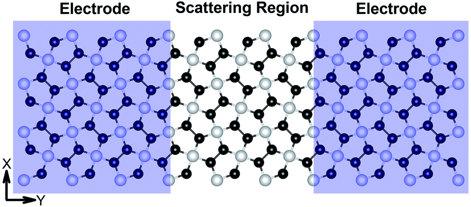
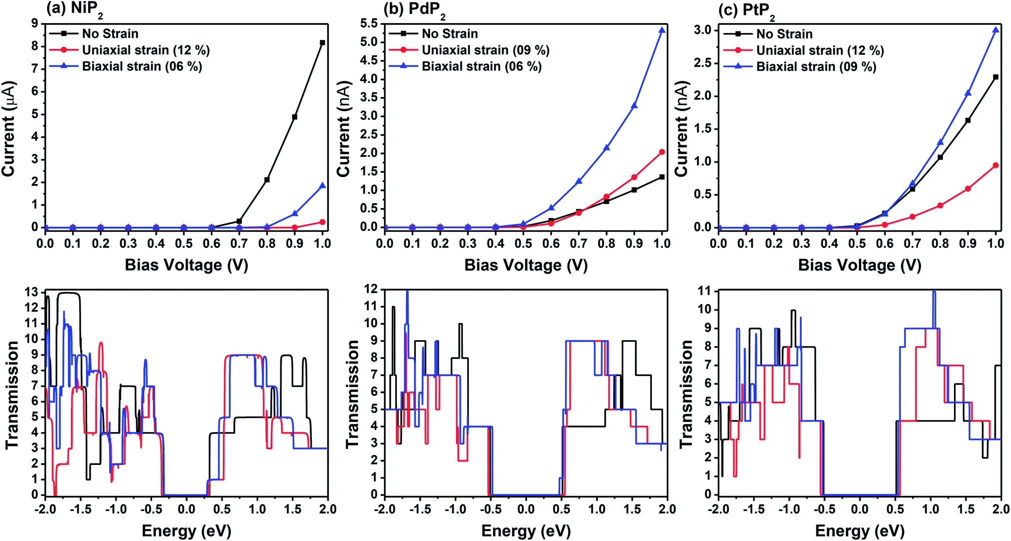
I–V responses and transmission spectra
Fig. 7 demonstrates a representation of the two-probe diagram for an electronic transport device for our considered penta-MP2 compounds, where two semi-infinite electrodes are coupled with the central scattering region; a 4 × 4 supercell is considered for both the left and right electrodes and for the centre scattering region as well. The 4 × 4 supercell geometry is considered to be the same as that found from the structural optimization and was also used for the electronic property calculations. The transport properties were calculated under the framework of NEGF methods. Fig. 8 illustrates the I–V characteristics of the penta-MP2 systems with and without tensile strain. It was found that for the NiP2 compound, although no current response was obtained up to an applied bias of 0.6 V, the response suddenly increased beyond 0.7 V and reached 8.2 μA at 1 V (Fig. 8(a)). Under the applied tensile strain, NiP2 do not show any significant impact, especially for the uniaxial strain. For the PdP2 and PtP2 compounds, as shown in Fig. 8(a and b), although no notable current was found until 0.5 V, remarkable transport was noted for both PdP2 and PtP2 beyond the applied bias of 0.5 V. In the case of the PdP2 compound, 1.5 and 4 times higher current flows (with 2.04 nA and 5.32 nA) at 1 V bias voltage were observed under applied uniaxial and biaxial strains, respectively, whereas for PtP2, 4.5 times lower response (0.51 nA) with uniaxial strain and 1.3 times enhancement (3 nA) in current were noted under the biaxial strain at 1 V bias voltage. Overall, it can be concluded that biaxial strain is significantly more effective than uniaxial strain for all the stretched penta-MP2 compounds in the present study. The lower vibrational (phonon) frequencies under biaxial strain compared to uniaxial strain may be a reason for these observations, which also accounts for the low thermal conductivity of these compounds. Further, Fig. 8 shows the zero-bias transmission coefficients as a function of energy before and after the applied strains on the penta-MP2 systems, where a noticeable effect of the applied tensile strains is observed. Although no significant changes under the tensile strains were noted near the Fermi level, minor transmission peaks for biaxial strain were observed in both the CBM and VBM regions. It should also be noted that biaxial stain shows similar transmission amplitude to the unstrained system, whereas comparatively low amplitude can be noted in the profile of uniaxial strain. The transmission response was found to be considerably high for the penta-MP2 compounds under biaxial strain in comparison to uniaxial strain.
 |
| | Fig. 7 Schematic of the model electronic device setup showing the semi-infinite left and right electrodes (violet-shaded regions) and the central scattering region. | |
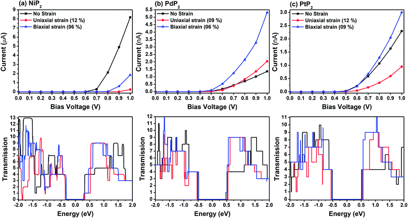 |
| | Fig. 8
I–V characteristics and zero-bias transmission spectra for unstrain and under axial tensile strain for the (a) NiP2, (b) PdP2 and (c) PtP2 compounds. | |
Optical properties of the strained penta-MP2 compounds
The optical properties of 2D penta-MP2 (M = Ni, Pd and Pt) monolayers under applied uniaxial and biaxial tensile strains are discussed in this section. The dynamical dielectric functions ε(ω) = ε′(ω) + ε′′(ω), including the real ε′(ω) and imaginary part ε′′(ω), were determined through HSE06 calculations. ε(ω) is divided into three parts based on the structural anisotropy, viz. the xx, yy and zz directions, with εxx = εyy ≠ εzz and εxx > εyy ≠ εzz for biaxial and uniaxial strains, respectively; therefore, one can understand the different behaviors of the incident light with the polarization of the electric field in-plane (parallel) and out-of-plane (perpendicular). For uniaxial strain, we considered only εxx for polarization in-plane (parallel) due to the accumulation of higher relative values than εyy. The spectra differ mainly due to the fact that ε(ω) is stronger in the parallel direction in the low energy range in the IR and visible ranges (0 to 3.5 eV), while ε(ω) intensifies in the perpendicular direction in the high energy UV range (3.5 to 10 eV) based on the blue shifts for the threshold peaks of ε(ω). Therefore, excitonic effects play an important role in the optical properties and dominate the performance of optoelectronic devices based on two-dimensional materials. The amounts of energy storage and dissipation within the medium are defined by the real ε′(ω) and imaginary ε′′(ω) parts, respectively. The ε′′(ω) is calculated as follows:76–78| | 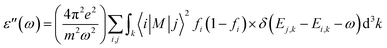 | (6) |
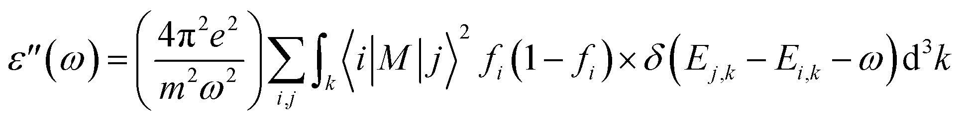
where ε, m, ω, and M denote the free electron charge, free electron mass, frequency of the incident photons and dipole matrix, receptively, i and j represent the initial and final states, respectively, fi is the Fermi distribution, and Ei is the free electron energy in the ith state with wave vector k.
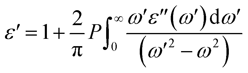
The real part of the dielectric function, ε′(ω), can be obtained using the Kramers–Kronig relationship as follows:77,79
| | 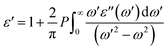 | (7) |
where
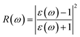
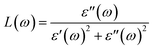
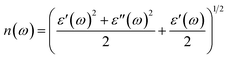
P represents the principal value of the integral. In addition to the dielectric function, we determined the absorption spectra
I(
ω), reflectivity
R(
ω), energy loss spectra
L(
ω) and refractive index
n(
ω) using the following equations:
80–82| |  | (8) |
| |  | (9) |
| |  | (10) |
| |  | (11) |
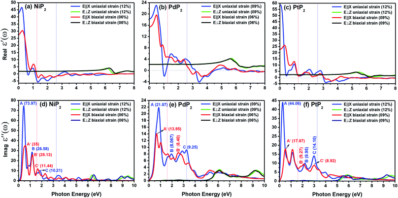
Fig. 9(a–c) present the profiles of the real parts of the dielectric constants of the penta-MP2 (M = Ni, Pd, and Pt) compounds under uniaxial (U) and biaxial (B) tensile strains. The calculated static dielectric constants ε′(ω) in the parallel direction with uniaxial (biaxial) strains are 20.24 (12.61), 18.07 (15.46) and 58.06 (22.64) for NiP2, PdP2 and PtP2, respectively; meanwhile, much lower polarizability was found in the perpendicular direction with the same applied uniaxial and biaxial strains, with values of 1.17, 2.07 and 2.33 for NiP2, PdP2 and PtP2, respectively. Also, the negative values in the dielectric constant of ε′(ω) indicate metallic nature for a particular amount of incident photon energy in the IR and visible spectra; the same nature was observed in the ultraviolet part of the electromagnetic spectrum. The dielectric constant of ε′(ω) was found to be negative at 0.68 eV (U), 1.37 eV (U) and 1.39 eV (Bi) for NiP2, 1.04 eV (U), 3.44 eV (U) and 3.65 eV (B) for PdP2, and 3.17 eV (U), 3.56 eV (B) for PtP2 in the parallel direction, while only positive values were observed for the polarization in the perpendicular direction of the electromagnetic (EM) spectrum.
 |
| | Fig. 9 Real and imaginary parts of the dielectric constants of the strained penta-MP2 (M = Ni, Pd, and Pt) compounds (a & d) NiP2, (b & e) PdP2, and (c & f) PtP2. | |
The electron–electron correlation is considered in the imaginary part of the dielectric function ε′′(ω) for stretched penta-MP2 compounds with the use of the HSE functional. In addition, the interactions between electrons and holes (e–h) mostly produce renormalization of the intensity of the optical peak obtained by the HSE functional. The major part of the imaginary dielectric constant ε′′(ω) shows interband transitions of electrons from the VBM to the CBM, and the bandgap is directly proportional to the energy of the interband transitions near the Fermi energy. It can be noted from Fig. 9(d–f) that the imaginary part of the dielectric constant ε′′(ω) shows dominant peaks near the band transition energy, as indicated by the peaks A(A′), B(B′) and C(C′) for the uniaxial (and biaxial) tensile strains. The first optical absorption peak was observed in the infrared region (IR) for all compounds, possessing high intensity; this peak showed a redshift in the parallel direction of polarization. This clearly indicates that the stretched penta-MP2 compounds are more sensitive in the IR region of the electromagnetic spectrum. In the IR region, the first peak A (uniaxial strain) is much higher than peak A′ (biaxial strain), and biaxial strain shows a blue shift in each case when light is polarized in the parallel direction of the electromagnetic spectrum. This can also be confirmed by the relatively large band gap values observed in the case of biaxial strain compared to uniaxial strain. The peak A(A′) of ε′′(ω) can be attributed to the interband transition of electrons from the valance band maximum (VBM) to the conduction band minimum (CBM). The second intense peak B(B′) also appears in the IR region for NiP2 and PtP2, whereas peak B(B′) shows a blue shift in the visible region for the PtP2 compound. The third peak C(C′) of ε′′(ω) is unveiled in the visible region for all the stretched penta-MP2 compounds, in which the slightly more intense peak is attributed to the biaxial strain of NiP2, and the remaining intense peaks show similar behavior in the PdP2 and PtP2 compounds. Because the photon energy for visible light ranges from 1.58 to 3.36 eV, this strongly suggests that the stretched penta-MP2 monolayers are also strong light-harvesting compounds. All the intense peaks were found to be along the parallel direction in the IR and visible regions for all the stretched penta-MP2 compounds, while the peaks along the perpendicular direction were found to be negligible. The light absorption coefficient expresses the percentage of light intensity attenuation per unit distance that is passed in the medium.
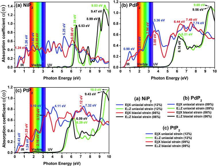
The optical absorption spectra can be understood by the decay of the incident light intensity spreading in a unit length, as shown in eqn (6). Fig. 10(a–c) shows the obtained absorption spectra for all the stretched penta-MP2 compounds to understand the excitation states at various incident energy levels of photons; obvious anisotropy can be observed along different polarization directions. Additionally, the absorption coefficient value reaches an order of 106 for all the cases under uniaxial and biaxial strains, which demonstrates high efficiency in the utilization of solar energy. The planar structure of penta-MP2 is mainly due to the interaction between the anti-bonding px–py π* orbital of P-dimer and the dx2–y2 orbital of the transition elements (Ni, Pd and Pt). The absorption spectra were found to be polarized in the parallel and perpendicular directions for the stretched penta-MP2 compounds due to the physical effects of the electron–electron (e–e) and electron–hole (e–h) interactions. The optical spectra are entirely re-shaped when the electron–hole interactions are included. The electron–hole interactions show variation when the polarization of light is in a different direction. Hence, the excitonic effect plays a significant role in the optical absorption spectra. A significant amount of optical transition was found at a lower energy range for tensile strain when the light was polarized along the parallel direction, while in the case of the perpendicular direction, optical transitions were found in the higher energy range. The intense absorption peaks are marked in the figure with the respective color of the polarization direction. For NiP2, the absorption peaks occur at energies of 1.19 eV (1.21 eV), 1.93 eV (2.23 eV) and 5.21 eV (6.07) in the parallel polarization direction, while for the perpendicular direction, intense peaks are observed only in the high energy region (UV), namely 6.40 eV (6.49 eV) and 9.54 eV (6.49) for uniaxial (biaxial) strain. For PdP2, the absorption peaks occur at energies of 0.96 eV, 2.09 eV (2.94 eV) and 3.37 eV (7.49) in the parallel polarization direction, while for the perpendicular direction, relatively high peaks are observed in the UV region of 9.56 eV (9.50 eV) for uniaxial (biaxial) strains. For the case of PtP2, the absorption peak arises at energies of 1.22 eV (1.21 eV), 2.30 eV (2.18 eV) and 3.10 eV (3.14) in the parallel polarization direction, whereas for the perpendicular direction, intense peaks are observed only in the higher energy region (UV) of 6.29 eV (9.97 eV) for uniaxial (biaxial) strain. It also can be observed that when the uniaxial strain for polarization was applied in the parallel or perpendicular directions, the optical absorption spectra were red shifted (lower energy range), while for the biaxial strain, blue shifts (higher energy) occurred in the optical absorption spectra. The optical absorption spectra reveal the appearance of stronger peaks in the IR and visible regions under the applied tensile strain compared to the unstrained penta-MP2 and other literature-reported penta compounds, e.g. PdAs2 and PdP2.33,34
 |
| | Fig. 10 The optical absorption spectra of the stretched penta-MP2 (M = Ni, Pd and Pt) compounds (a) NiP2, (b) PdP2, and (c) PtP2. | |
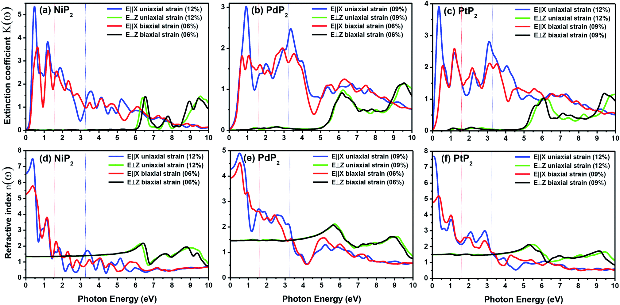
The extinction coefficients and the refraction indices of the stretched penta-MP2 compounds are illustrated in Fig. 11. It can be noted from the Fig. 11(a–c) that the first local extinction coefficient K(ω) maxima in the parallel direction are positioned at 0.47 eV (0.59 eV), 0.85 eV (0.72 eV) and 0.33 eV (1.21 eV) for uniaxial (biaxial) strains, corresponding to the NiP2, PdP2 and PtP2 compounds, and more intense peaks were observed in the IR region for uniaxial strain compared to biaxial strain. The second intense peaks of the extinction coefficient are located at 1.21 eV (1.21 eV), 3.30 eV (2.90 eV) and 1.19 eV (1.19 eV) for uniaxial (biaxial) strains corresponding to NiP2, PdP2 and PtP2. These intense peaks reveal the maximum absorptions in the medium. The photons are absorbed very rapidly in these energy regions. The respective intense peaks in the extinction coefficients have maximum absorption spectra, as presented in Fig. 10(a–c). The static refractive index at 0 eV was found to have the same value of ∼1.5 for all the stretched compounds with polarization in the perpendicular direction, while distinct differences can be observed for the polarization in the parallel direction under uniaxial and biaxial strains. In the parallel direction, the static refractive index under biaxial strain shows lower values than under uniaxial strain, namely 6.50 eV (5.22 eV), 4.26 eV (3.92 eV) and 7.70 eV (4.77 eV) for NiP2, PdP2 and PtP2, respectively. The refractive index n(ω) in the IR region appears to decrease rapidly with the energy in the parallel direction, whereas it remained steady in the UV region after 7.0 eV, as shown in Fig. 11(d–f). The refractive index was found to be less than 1 over a number of frequencies in the electromagnetic spectrum; this indicates a lower value of light celerity c than the light phase velocity, in dissimilarity with the relativity. The signal propagates with the group velocity vg = dω/dk rather than with the phase velocity (v) in a dispersive medium. The relationship between vg and v is  , which indicates that vg is always a lower value than v.81 In the perpendicular direction, it was found to increase slightly monotonically near the UV region, and after fluctuations, it decreased in the far UV region and became constant after ∼15 eV.
 |
| | Fig. 11 Extinction coefficients and refractive indices of the stretched penta-MP2 (M = Ni, Pd and Pt) compounds (a & d) NiP2, (b & e) PdP2, and (c & f) PtP2. | |
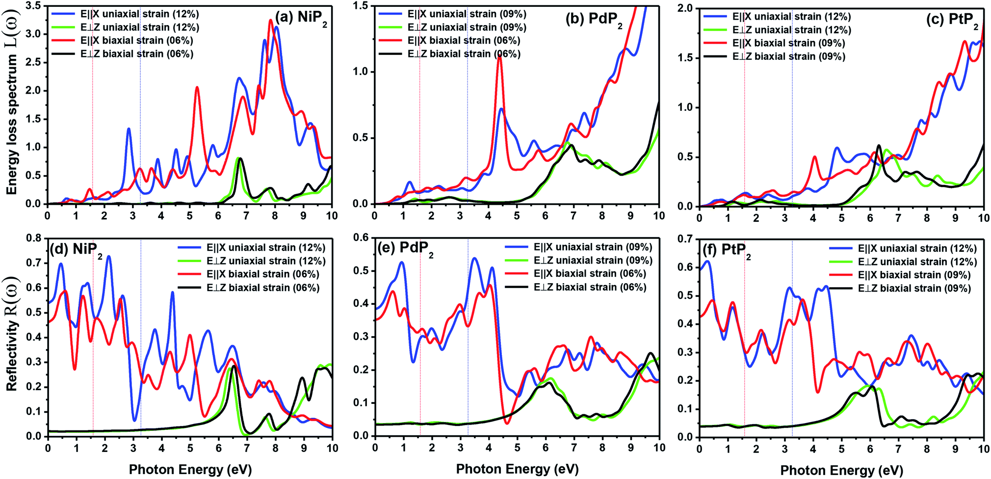
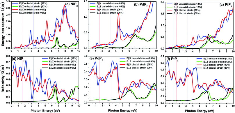
The electron energy loss spectrum (EELS) refers to the amount of energy that electrons lose when passing through a dielectric medium, and this can be used to deduce the dielectric functions of materials. The EELS is illustrated in Fig. 12(a–c) as a function of the photon energy for the stretched penta-MP2 compounds for the polarization along the parallel and perpendicular directions. The calculated energy loss spectrum L(ω) for NiP2 was found to be quite large at 2.9 eV photon energy (uniaxial direction), whereas a much lower peak was observed at 1.4 eV (biaxial strain) for the polarization in the parallel direction. There are several peaks of EELS, which suggests that the photon loses energy above 4 eV, and resonance is visible in the ultraviolet region. Biaxial strain showed higher EELS peaks compared to uniaxial strain for the polarization along the parallel and perpendicular directions for all the penta-MP2 compounds. Intense peaks were observed at 5.34 eV and 7.81 eV for NiP2, 4.34 eV and 9.17 eV for PdP2, and 4.08 eV and 9.35 eV for PtP2 in the parallel direction, while the maxima in the perpendicular direction were found to be 6.81 eV, 6.67 eV and 6.30 eV for NiP2, PdP2 and PtP2, respectively. The lower effect of the EELS below 3.5 eV strongly suggests that our compounds are more subtle in the IR and visible regions.
 |
| | Fig. 12 Electron energy loss spectra (EELS) and reflectivities of the stretched penta-MP2 (M = Ni, Pd, and Pt) compounds (a & d) NiP2, (b & e) PdP2, and (c & f) PtP2. | |
The reflectivities R(ω) of the stretched penta-MP2 compounds in both directions of polarization are demonstrated in Fig. 12(d–f), which specifies how many photons are reflected from the material and incident on the material. For all photon energies, the reflection was found to be much higher in the parallel direction due to stronger optical excitation than in the vertical direction for all compounds. In comparison to the PdP2 and PtP2 compounds, the maximum reflectivities were observed in the NiP2 compound to be 70% (57%), 73% (54%) and 58% (40%) for uniaxial (biaxial) strains in the electromagnetic spectra. Taking into account the above observations, NiP2 appears to be a much better IR and visible light absorber, while PdP2 and PtP2 are appropriate as IR and UV light absorbers. Overall, due to the higher reflectivity and considerable absorption in the IR and visible regions, NiP2 appears to be a non-transparent material. Moreover, the quite low adsorption peaks (Fig. 10) and high reflectivity peaks (Fig. 12(d–f)) in the IR region of the spectrum for all the stretched penta-MP2 compounds suggest that these compounds will not absorb much heat, and they can be used as good hot mirrors for application in heat control, environmental protection, coatings, etc.83–85 For the sake of completeness, we also calculated the optical properties of the penta-MP2 (M = Ni, Pd and Pt) monolayers without strain, as presented in Fig. S8 (ESI†), for comparison. In the case of the stretched penta-MP2 compounds, we observed some additional adsorption peaks in the IR region, whereas the intensity of the peaks increased in the visible region after the application of uniaxial strain in comparison to the unstrained penta-MP2 case.
Concluding remarks
In summary, the structural, electronic, I–V and optical properties of the stretched penta-MP2 (M = Ni, Pd and Pt) compounds were systematically investigated in detail using first-principles calculations. The present investigation reveals that the application of uniaxial and biaxial strains enhances the energy band gap significantly for the considered penta-MP2 compounds, which possess nearly zero band gaps in their original state. Our results show that under optimum amounts of applied uniaxial and biaxial strain, the band gap appears to be maximal, after which the materials proceed toward metallic nature. The stability of the considered penta-MP2 compounds under strain was confirmed through phonon dispersion and elastic coefficient analyses. The implementation of HSE06 calculations for determining the electronic and optical properties provides more reliability in the obtained results. The I–V characteristics of the stretched penta-MP2 compounds show better transport characteristics than the unstretched systems for the PdP2 and PtP2 systems. The electronic and optical properties of penta-MP2 were found to be modulated effectively by tensile strains through the changes in the p orbitals of the P atom and the dx–dy orbital of the transition element (Ni, Pd or Pt). The optical absorption spectra for all the compounds reached 106 cm−1 under the applied strains, and intense peaks were found in the IR and visible region, which indicates the possible usage of these materials for high performance solar energy and good hot mirror material applications. The higher reflectivity and considerable absorption in the IR and visible regions suggest the non-transparent nature of the considered penta-MP2 materials. The outcomes of the present investigation not only reflect great potential applications for the stretched penta-MP2 compounds as ultra-thin reflectors and good absorbers for optoelectronic applications, but may also direct the discovery of new optical information and realization of various optical functions in specific frequency ranges of the electromagnetic spectrum. The developed penta-MP2 monolayers can also be used as good hot mirrors in various applications, such as heat control, environmental protection, and coatings.
Conflicts of interest
The authors declare that they have no conflict of interest.
Acknowledgements
DRR is thankful to the SERB, New Delhi, Govt. of India for financial support (Grant No. EMR/2016/005830). DRR is also thankful to Hanse-Wissenschaftskolleg (HWK), Delmenhorst, Germany, for his regular fellowship. DRR and VK are also thankful for the High-Performance Computing facility at Centre for Development of Advanced Computing (CDAC), Pune, India.
References
- K. S. Novoselov, A. K. Geim, S. V. Morozov, D. Jiang, Y. Zhang, S. V. Dubonos, I. V. Grigorieva and A. A. Firsov, Science, 2004, 306, 666–669 CrossRef CAS.
- A. C. Ferrari, F. Bonaccorso, V. Fal'ko, K. S. Novoselov, S. Roche, P. Bøggild, S. Borini, F. H. L. Koppens, V. Palermo, N. Pugno, J. A. Garrido, R. Sordan, A. Bianco, L. Ballerini, M. Prato, E. Lidorikis, J. Kivioja, C. Marinelli, T. Ryhänen, A. Morpurgo, J. N. Coleman, V. Nicolosi, L. Colombo, A. Fert, M. Garcia-Hernandez, A. Bachtold, G. F. Schneider, F. Guinea, C. Dekker, M. Barbone, Z. Sun, C. Galiotis, A. N. Grigorenko, G. Konstantatos, A. Kis, M. Katsnelson, L. Vandersypen, A. Loiseau, V. Morandi, D. Neumaier, E. Treossi, V. Pellegrini, M. Polini, A. Tredicucci, G. M. Williams, B. H. Hong, J.-H. Ahn, J. M. Kim, H. Zirath, B. J. van Wees, H. van der Zant, L. Occhipinti, A. D. Matteo, I. A. Kinloch, T. Seyller, E. Quesnel, X. Feng, K. Teo, N. Rupesinghe, P. Hakonen, S. R. T. Neil, Q. Tannock, T. Löfwander and J. Kinaret, Nanoscale, 2015, 7, 4598–4810 RSC.
- K. S. Novoselov, V. I. Fal′ko, L. Colombo, P. R. Gellert, M. G. Schwab and K. Kim, Nature, 2012, 490, 192–200 CrossRef CAS.
- Y. Zhang, Y.-W. Tan, H. L. Stormer and P. Kim, Nature, 2005, 438, 201–204 CrossRef CAS.
- A. A. Balandin, Nat. Mater., 2011, 10, 569–581 CrossRef CAS.
- J. Hu, B. Xu, C. Ouyang, S. A. Yang and Y. Yao, J. Phys. Chem. C, 2014, 118, 24274–24281 CrossRef CAS.
- L. Lindsay, D. A. Broido and N. Mingo, Phys. Rev. B: Condens. Matter Mater. Phys., 2010, 82, 115427 CrossRef.
- A. C. Ferrari, F. Bonaccorso, V. Fal'ko, K. S. Novoselov, S. Roche, P. Bøggild, S. Borini, F. H. L. Koppens, V. Palermo, N. Pugno, J. A. Garrido, R. Sordan, A. Bianco, L. Ballerini, M. Prato, E. Lidorikis, J. Kivioja, C. Marinelli, T. Ryhänen, A. Morpurgo, J. N. Coleman, V. Nicolosi, L. Colombo, A. Fert, M. Garcia-Hernandez, A. Bachtold, G. F. Schneider, F. Guinea, C. Dekker, M. Barbone, Z. Sun, C. Galiotis, A. N. Grigorenko, G. Konstantatos, A. Kis, M. Katsnelson, L. Vandersypen, A. Loiseau, V. Morandi, D. Neumaier, E. Treossi, V. Pellegrini, M. Polini, A. Tredicucci, G. M. Williams, B. H. Hong, J.-H. Ahn, J. M. Kim, H. Zirath, B. J. van Wees, H. van der Zant, L. Occhipinti, A. D. Matteo, I. A. Kinloch, T. Seyller, E. Quesnel, X. Feng, K. Teo, N. Rupesinghe, P. Hakonen, S. R. T. Neil, Q. Tannock, T. Löfwander and J. Kinaret, Nanoscale, 2015, 7, 4598–4810 RSC.
- M. Rejhon, J. Franc, V. Dědič, P. Hlídek and J. Kunc, J. Phys. D: Appl. Phys., 2018, 51, 265104 CrossRef.
- S. Hu, M. Lozada-Hidalgo, F. C. Wang, A. Mishchenko, F. Schedin, R. R. Nair, E. W. Hill, D. W. Boukhvalov, M. I. Katsnelson, R. a. W. Dryfe, I. V. Grigorieva, H. A. Wu and A. K. Geim, Nature, 2014, 516, 227–230 CrossRef CAS.
- M. Yagmurcukardes, H. Sahin, J. Kang, E. Torun, F. M. Peeters and R. T. Senger, J. Appl. Phys., 2015, 118, 104303 CrossRef.
- X. Zhang, H. Xie, M. Hu, H. Bao, S. Yue, G. Qin and G. Su, Phys. Rev. B: Condens. Matter Mater. Phys., 2014, 89, 054310 CrossRef.
- P. Vogt, P. De Padova, C. Quaresima, J. Avila, E. Frantzeskakis, M. C. Asensio, A. Resta, B. Ealet and G. Le Lay, Phys. Rev. Lett., 2012, 108, 155501 CrossRef.
- M. Houssa, A. Dimoulas and A. Molle, J. Phys.: Condens. Matter, 2015, 27, 253002 CrossRef CAS.
- L. Li, Y. Yu, G. J. Ye, Q. Ge, X. Ou, H. Wu, D. Feng, X. H. Chen and Y. Zhang, Nat. Nanotechnol., 2014, 9, 372–377 CrossRef CAS.
- H. Liu, A. T. Neal, Z. Zhu, Z. Luo, X. Xu, D. Tománek and P. D. Ye, ACS Nano, 2014, 8, 4033–4041 CrossRef CAS.
- K. F. Mak, C. Lee, J. Hone, J. Shan and T. F. Heinz, Phys. Rev. Lett., 2010, 105, 136805 CrossRef.
- H. S. S. Ramakrishna Matte, A. Gomathi, A. K. Manna, D. J. Late, R. Datta, S. K. Pati and C. N. R. Rao, Angew. Chem., Int. Ed., 2010, 49, 4059–4062 CrossRef.
- S. Zhang, J. Zhou, Q. Wang, X. Chen, Y. Kawazoe and P. Jena, Proc. Natl. Acad. Sci. U. S. A., 2015, 112(8), 2372–2377 CrossRef CAS.
- H. Liu, G. Qin, Y. Lin and M. Hu, Nano Lett., 2016, 16, 3831–3842 CrossRef CAS.
- G. R. Berdiyorov and M. E.-A. Madjet, RSC Adv., 2016, 6, 50867–50873 RSC.
- H. Liu, A. T. Neal, Z. Zhu, Z. Luo, X. Xu, D. Tománek and P. D. Ye, ACS Nano, 2014, 8, 4033–4041 CrossRef CAS.
- Y. Jing, Y. Ma, Y. Li and T. Heine, Nano Lett., 2017, 17, 1833–1838 CrossRef CAS.
- N. Miao, B. Xu, N. C. Bristowe, J. Zhou and Z. Sun, J. Am. Chem. Soc., 2017, 139, 11125–11131 CrossRef CAS.
- W. Yi, X. Chen, Z. Wang, Y. Ding, B. Yang and X. Liu, J. Mater. Chem. C, 2019, 7, 7352–7359 RSC.
- B. Ghosh, S. Puri, A. Agarwal and S. Bhowmick, J. Phys. Chem. C, 2018, 122, 18185–18191 CrossRef CAS.
- S. Sun, F. Meng, H. Wang, H. Wang and Y. Ni, J. Mater. Chem. A, 2018, 6, 11890–11897 RSC.
- N. Lu, Z. Zhuo, H. Guo, P. Wu, W. Fa, X. Wu and X. C. Zeng, J. Phys. Chem. Lett., 2018, 9, 1728–1733 CrossRef CAS.
- A. D. Oyedele, S. Yang, L. Liang, A. A. Puretzky, K. Wang, J. Zhang, P. Yu, P. R. Pudasaini, A. W. Ghosh, Z. Liu, C. M. Rouleau, B. G. Sumpter, M. F. Chisholm, W. Zhou, P. D. Rack, D. B. Geohegan and K. Xiao, J. Am. Chem. Soc., 2017, 139, 14090–14097 CrossRef CAS.
- F. Shojaei, J. R. Hahn and H. S. Kang, J. Mater. Chem. A, 2017, 5, 22146–22155 RSC.
- Y. Ding and Y. Wang, J. Mater. Chem. C, 2015, 3, 11341–11348 RSC.
- H. Liu, G. Qin, Y. Lin and M. Hu, Nano Lett., 2016, 16, 3831–3842 CrossRef CAS.
- H. Yuan, Z. Li and J. Yang, J. Mater. Chem. C, 2018, 6, 9055–9059 RSC.
- S. Qian, X. Sheng, X. Xu, Y. Wu, N. Lu, Z. Qin, J. Wang, C. Zhang, E. Feng, W. Huang and Y. Zhou, J. Mater. Chem. C, 2019, 7, 3569–3575 RSC.
- S. Furuseth, K. Selte, A. Kjekshus, S. Gronowitz, R. A. Hoffman and A. Westerdahl, Acta Chem. Scand., 1965, 19, 257–258 CrossRef CAS.
- J. Qi, X. Li, X. Qian and J. Feng, Appl. Phys. Lett., 2013, 102, 173112 CrossRef.
- K. Wang, T. Hu, F. Jia, G. Zhao, Y. Liu, I. V. Solovyev, A. P. Pyatakov, A. K. Zvezdin and W. Ren, Appl. Phys. Lett., 2019, 114, 092405 CrossRef.
- Q. Liu, L. Li, Y. Li, Z. Gao, Z. Chen and J. Lu, J. Phys. Chem. C, 2012, 116, 21556–21562 CrossRef CAS.
- P. Johari and V. B. Shenoy, ACS Nano, 2012, 6, 5449–5456 CrossRef CAS.
- N. Lu, H. Guo, L. Li, J. Dai, L. Wang, W.-N. Mei, X. Wu and X. C. Zeng, Nanoscale, 2014, 6, 2879–2886 RSC.
- C. Lee, X. Wei, J. W. Kysar and J. Hone, Science, 2008, 321, 385–388 CrossRef CAS.
- J. Wang, F. Sansoz, J. Huang, Y. Liu, S. Sun, Z. Zhang and S. X. Mao, Nat. Commun., 2013, 4, 1–8 CAS.
- J. Pokluda, M. Černý, P. Šandera and M. Šob, J. Comput.-Aided Mater. Des., 2004, 11, 1–28 CrossRef.
- F. Liu, P. Ming and J. Li, Phys. Rev. B: Condens. Matter Mater. Phys., 2007, 76, 064120 CrossRef.
- Z. Zhu and D. Tománek, Phys. Rev. Lett., 2014, 112, 176802 CrossRef.
- S. Zhang, Z. Yan, Y. Li, Z. Chen and H. Zeng, Angew. Chem., Int. Ed., 2015, 54, 3112–3115 CrossRef CAS.
- G. Wang, R. Pandey and S. P. Karna, ACS Appl. Mater. Interfaces, 2015, 7, 11490–11496 CrossRef CAS.
- C. Kamal and M. Ezawa, Phys. Rev. B: Condens. Matter Mater. Phys., 2015, 91, 085423 CrossRef.
- S. Zhang, M. Xie, F. Li, Z. Yan, Y. Li, E. Kan, W. Liu, Z. Chen and H. Zeng, Angew. Chem., Int. Ed., 2016, 55, 1666–1669 CrossRef CAS.
- N. Argaman and G. Makov, Am. J. Phys., 1999, 68, 69–79 CrossRef.
- J. P. Perdew, K. Burke and M. Ernzerhof, Phys. Rev. Lett., 1996, 77, 3865–3868 CrossRef CAS.
- J. P. Perdew, K. Burke and M. Ernzerhof, Phys. Rev. Lett., 1997, 78, 1396 CrossRef CAS.
- J. Heyd, G. E. Scuseria and M. Ernzerhof, J. Chem. Phys., 2006, 124, 219906 CrossRef.
- J. Heyd, G. E. Scuseria and M. Ernzerhof, J. Chem. Phys., 2003, 118, 8207–8215 CrossRef CAS.
- G. Kresse and J. Furthmüller, Comput. Mater. Sci., 1996, 6, 15–50 CrossRef CAS.
- G. Kresse and J. Hafner, Phys. Rev. B: Condens. Matter Mater. Phys., 1994, 49, 14251–14269 CrossRef CAS.
- G. Kresse and J. Furthmüller, Comput. Mater. Sci., 1996, 6, 15–50 CrossRef CAS.
- G. Kresse and J. Furthmüller, Phys. Rev. B: Condens. Matter Mater. Phys., 1996, 54, 11169–11186 CrossRef CAS.
- G. Kresse and D. Joubert, Phys. Rev. B: Condens. Matter Mater. Phys., 1999, 59, 1758–1775 CrossRef CAS.
- P. E. Blöchl, Phys. Rev. B: Condens. Matter Mater. Phys., 1994, 50, 17953–17979 CrossRef.
- J. Heyd and G. E. Scuseria, J. Chem. Phys., 2004, 121, 1187–1192 CrossRef CAS.
- A. V. Krukau, O. A. Vydrov, A. F. Izmaylov and G. E. Scuseria, J. Chem. Phys., 2006, 125, 224106 CrossRef.
-
P. Giannozzi and S. Baroni, in Handbook of Materials Modeling: Methods, ed. S. Yip, Springer Netherlands, Dordrecht, 2005, pp. 195–214 Search PubMed.
- A. Togo and I. Tanaka, Scr. Mater., 2015, 108, 1–5 CrossRef CAS.
- K. Momma and F. Izumi, J. Appl. Crystallogr., 2008, 41, 653–658 CrossRef CAS.
- M. Büttiker, Phys. Rev. Lett., 1986, 57, 1761–1764 CrossRef.
- M. Brandbyge, J.-L. Mozos, P. Ordejón, J. Taylor and K. Stokbro, Phys. Rev. B: Condens. Matter Mater. Phys., 2002, 65, 165401 CrossRef.
-
S. Datta, Electronic Transport in Mesoscopic Systems,/core/books/electronic-transport-in-mesoscopic-systems/1E55DEF5978AA7B843FF70337C220D8B, accessed April 13, 2020 Search PubMed.
- M. Naguib and Y. Gogotsi, Acc. Chem. Res., 2015, 48, 128–135 CrossRef CAS.
- M. Naguib, M. Kurtoglu, V. Presser, J. Lu, J. Niu, M. Heon, L. Hultman, Y. Gogotsi and M. W. Barsoum, Adv. Mater., 2011, 23, 4248–4253 CrossRef CAS.
- F. Mouhat and F.-X. Coudert, Phys. Rev. B: Condens. Matter Mater. Phys., 2014, 90, 224104 CrossRef.
- Y. Le Page and P. Saxe, Phys. Rev. B: Condens. Matter Mater. Phys., 2002, 65, 104104 CrossRef.
- M. N. Blonsky, H. L. Zhuang, A. K. Singh and R. G. Hennig, ACS Nano, 2015, 9, 9885–9891 CrossRef CAS.
- Y. Ding and Y. Wang, J. Phys. Chem. C, 2013, 117, 18266–18278 CrossRef CAS.
- V. Wang and W. T. Geng, J. Phys. Chem. C, 2017, 121, 10224–10232 CrossRef CAS.
- T. Puangmali, M. Califano and P. Harrison, Phys. Rev. B: Condens. Matter Mater. Phys., 2008, 78, 245104 CrossRef.
- C. Ambrosch-Draxl and J. O. Sofo, Comput. Phys. Commun., 2006, 175, 1–14 CrossRef CAS.
- P. Puschnig and C. Ambrosch-Draxl, Phys. Rev. B: Condens. Matter Mater. Phys., 2002, 66, 165105 CrossRef.
- P. Y. Yu and M. Cardona, J. Phys. Soc. Jpn., 1998, 53, 359–360 Search PubMed.
- S. Saha, T. P. Sinha and A. Mookerjee, Phys. Rev. B: Condens. Matter Mater. Phys., 2000, 62, 8828–8834 CrossRef CAS.
-
M. Fox, Optical Properties of Solids, Oxford University Press, Oxford, New York, 2nd edn, 2010 Search PubMed.
- D. W. Reitz, Mater. Manuf. Processes, 2005, 20, 1005 CrossRef.
- D. Singh, S. K. Gupta, Y. Sonvane and I. Lukačević, J. Mater. Chem. C, 2016, 4, 6386–6390 RSC.
- X. Yang, D. Singh, Z. Xu, Z. Wang and R. Ahuja, J. Mater. Chem. C, 2019, 7, 12312–12320 RSC.
- V. S. Kaluba, K. Mohamad and P. Ferrer, Appl. Energy, 2020, 257, 114020 CrossRef.
Footnotes |
| † Electronic supplementary information (ESI) available. See DOI: 10.1039/d0na00503g |
| ‡ Present address: Department of Chemistry, University of Ulsan, Ulsan 44776, Republic of Korea. |
|
| This journal is © The Royal Society of Chemistry 2020 |
Click here to see how this site uses Cookies. View our privacy policy here. 
 Open Access Article
 This Open Access Article is licensed under a
  *a and
Debesh R.
Roy
*a and
Debesh R.
Roy


 , which indicates that vg is always a lower value than v.81 In the perpendicular direction, it was found to increase slightly monotonically near the UV region, and after fluctuations, it decreased in the far UV region and became constant after ∼15 eV.