
 Open Access Article
 This Open Access Article is licensed under a Creative Commons Attribution-Non Commercial 3.0 Unported Licence
A non-oxidizing fabrication method for lithographic break junctions of sensitive metals
Anna
Nyáry†
ab,
Agnes
Gubicza†
 ac,
Jan
Overbeck
cd,
László
Pósa
ae,
Péter
Makk
af,
Michel
Calame
cdf,
András
Halbritter
*ab and
Miklós
Csontos
ac
ac,
Jan
Overbeck
cd,
László
Pósa
ae,
Péter
Makk
af,
Michel
Calame
cdf,
András
Halbritter
*ab and
Miklós
Csontos
ac
aDepartment of Physics, Budapest University of Technology and Economics, Budafoki út 8, 1111 Budapest, Hungary. E-mail: halbritt@mail.bme.hu
bMTA-BME Condensed Matter Research Group, Budafoki út 8, 1111 Budapest, Hungary
cEmpa, Swiss Federal Laboratories for Materials Science and Technology, Transport at Nanoscale Interfaces Laboratory, Überlandstrasse 129, CH-8600 Dübendorf, Switzerland
dSwiss Nanoscience Institute, University of Basel, Klingelbergstrasse 82, CH-4056 Basel, Switzerland
eInstitute of Technical Physics and Materials Science, Centre for Energy Research, Konkoly-Thege M. út 29-33, 1121 Budapest, Hungary
fDepartment of Physics, University of Basel, Klingelbergstrasse 82, CH-4056 Basel, Switzerland
First published on 24th July 2020
Abstract
Electrochemically active metals offer advanced functionalities with respect to the well-established gold electrode arrangements in various electronic transport experiments on atomic scale objects. Such functionalities can arise from stronger interactions with the leads which provide better coupling to specific molecules and may also facilitate metallic filament formation in atomic switches. However, the higher reactivity of the electrode metal also imposes challenges in the fabrication and reliability of nanometer scale platforms, limiting the number of reported applications. Here we present a high-yield lithographic fabrication procedure suitable to extend the experimental toolkit with mechanically controllable break junctions of oxygen sensitive metallic electrodes. We fabricate and characterize silver break junctions exhibiting single-atomic conductance and superior mechanical and electrical stability at room temperature. As a proof-of-principle application, we demonstrate resistive switching between metastable few-atom configurations at finite voltage bias.
The mechanically controllable break junction (MCBJ) technique1,2 has become a versatile tool to study conduction phenomena at the ultimate single-atom3–6 or single-molecule7–12 level. The rupture of a metallic wire in a three-point bending configuration in the MCBJ arrangement grants a superior mechanical stability to atomic-scale junctions as compared to scanning tunneling microscope-based break junctions. Additionally, the cleanliness of the freshly broken electrode surfaces provides another major advantage. The MCBJ technique was further improved by replacing hand-made, notched-wire devices with nanofabricated metallic bridges.2,13 Thereby an electrode displacement to an actuation ratio up to 104–106 can be achieved, i.e. a micron-scale mechanical noise in the direct actuation is reduced to a sub-Ångstrom displacement noise in the studied atomic-scale structure. This extreme stability was utilized to stabilize single-atom and single-molecule structures for unprecedentedly long times up to days, enabling a broad variety of demanding quantum transport measurements.4,14–20 Furthermore, the nanofabricated approach allows the combination of complex on-chip nanocircuits relying on ultra-fine mechanical actuation. As an example, superconducting quantum interferometer devices (SQUIDs) were established, where one arm of the SQUID was an adjustable single-atom contact.21–23 However, the nanofabrication approach poses severe limitations on the electrode material selection. In particular, most of the metals are incompatible with the standard fabrication template due to the degradation of the electrodes during the suspension step executed by oxygen plasma etching.
Here we present a plasma-free lithographic procedure to fabricate MCBJ devices. Our method relies on an alternative technique utilizing the suspension of the metal bridge by standard electron beam lithography carried out on a LOR™ substrate. By eliminating the exposure of the reactive metal surfaces to oxygen beyond the ambient atmosphere, our method is suitable to realize MCBJs with a broad range of oxygen sensitive metallic compounds. In particular, silver is a versatile electrode material for both single-molecule electronics24–30 and for resistive switching memory devices.31–45 Therefore we demonstrate the merits of the proposed approach by investigating nanofabricated silver break junctions which were so-far inaccessible due to their extreme sensitivity to oxygen plasma treatment. We benchmark our devices through the pronounced single-atom peak emerging in the measured conductance histogram. Furthermore, we demonstrate room temperature current-induced atomic switching between few-atom configurations, similar to the low-temperature measurements of Al nanofabricated MCBJ devices17 and room temperature studies of Au MCBJs.46
The suspended Ag nanobridges were fabricated on bendable, 0.3 mm thick stainless steel substrates by multiple electron beam lithography steps as illustrated in Fig. 1. The fabrication was performed on top of a polydimethylglutarimide based LOR™ layer which was removed from below the Ag bridge in the last fabrication step. Below we outline in detail the fabrication procedure which was inspired by the similar method developed for suspending graphene nanostructures.47–53 First, the stainless steel plate was coated with an insulating polyimide layer of 4 μm thickness. The latter was achieved by repeated, alternating steps of spin coating at 4000 rpm for 30 s and baking at 300 °C for 1 hour. Next, a 300 nm thick LOR™ 3A layer was spun on the top of polyimide at 4000 rpm for 45 s followed by 15 minutes baking at 200 °C. This serves as a sacrificial layer which will later be removed for the suspension of the Ag break junction. Finally, the substrate was coated with a 430 nm thick PMMA 950 K AR-P 671.04 layer, serving as the electron-beam resist mask of the hour-glass shaped Ag structure. The first electron beam lithography (EBL) step shown in Fig. 1(a) was carried out using 20 keV electrons, a line dose of 1000 pC cm−1 in the bridge area and an area dose of 190–240 μC cm−2 in the electrode region. PMMA development was performed in o-xylene for 110 s and stopped in hexane at room temperature [Fig. 1(b)]. Next, a 70 nm thick Ag layer was evaporated [Fig. 1(c)] followed by lift-off in 70 °C o-xylene and rinsing in room temperature hexane, resulting in the desired shape of the lateral Ag structure [Fig. 1(d)]. The replacement of the standard PMMA lift-off solvents acetone and isopropanol by the above chemicals was essential to avoid damages both to LOR™ and Ag. During evaporation Cr or Ti buffer layers were avoided as these could influence the transport through the single atom contacts.
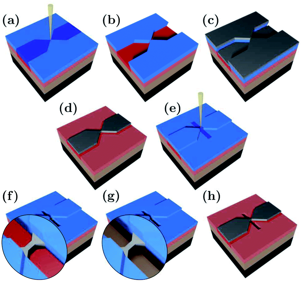 | ||
| Fig. 1 (a)–(h) The three-dimensional illustration of the adjacent fabrication steps of the suspended Ag nanobridge. Stainless steel (black), polyimide (light brown), LOR™ (pink), PMMA (blue), and Ag (grey). The resist regions exposed during electron beam lithography are marked with saturated colors. See the text for details. | ||
We note, that due to the small dose of the scattered electrons released during standard electron beam evaporation of Ag, the LOR™ layer is unintentionally exposed over the entire sample surface. In addition to its controlled exposure under the final Ag structure executed during the first EBL step, this effect can lead to the removal of the LOR™ layer under the leads during the suspension step, resulting in the mechanical instability of the junction. Such a device failure can be prevented by the application of the less widely available thermal evaporation of Ag. As an alternative approach, our samples were coated with a 70 nm thick layer of PMMA 950 K AR-P 671.02 [Fig. 1(e)] which served as a protection mask for the leads during the suspension step. Thereby the removal of the sacrificial LOR™ layer in the final suspension step is restricted to the desired area right under the metal constriction, whereas the undesired removal of the partially exposed LOR™ under the leads is prevented. Thus, the safe use of the more widely available electron beam evaporation technique is enabled without compromising the mechanical stability of the exposed but undeveloped LOR™ support.
The trench for the suspension was defined by exposure to 20 keV electrons at an area dose of 1200 μC cm−2. Within this area the PMMA and the underlying LOR™ were removed during 110 s of development in o-xylene [Fig. 1(f)] and during 120 s of development in 1-methoxy-2-propanol [Fig. 1(g)], respectively. Each development phase was stopped by rinsing in hexane for 30 s. Finally, the rest of the PMMA layer was removed by immersing the sample in 70 °C o-xylene for 5 minutes and a subsequent rinsing in hexane [Fig. 1(h)]. We note, that beside the elimination of the traditional oxygen plasma etching step, no critical point drying was needed for the suspension, either.
The Ag MCBJs and the two-terminal conductance measurement setup are schematically illustrated in Fig. 2(a). A representative electron microscopy image of the Ag bridge is also shown in the inset. A statistical image analysis revealed a 100 ± 20 nm width and 140 ± 50 nm length at the narrowest cross-section of the as-fabricated junctions. The length of the suspended region was 880 ± 200 nm. In the experiments, the yield of the functional devices was further increased by adding multiple, simultaneously fabricated junctions to the same substrate in the arrangement of a shared electrode on one side. The bending of the substrate was actuated by a step motor controlled via the feedback of real-time current measurements at the junction. Conductance measurements were carried out as a function of the electrode displacement by the application of a small Vdrive voltage to the junction and an RS series resistor. The latter helped to protect the initial nanowire with ≈100 Ω resistance against unwanted electrical breakdown. The current was monitored with a Femto DLPCA200 current amplifier at 105 gain setting. All measurements were carried out at room temperature under 10−3 mbar base pressure.
 | ||
| Fig. 2 (a) The schematics of the electrical transport measurement layout and the three-dimensional illustration of the MCBJ setup. RS = 1050 Ω and Vdrive = 10 mV for all measurements. The inset shows the electron beam microscopy image of an as-prepared junction. The white scale bar corresponds to 1 μm. (b) Selected conductance traces recorded during breaking as a function of the electrode displacement. The traces are horizontally off-set for clarity. (c) Conductance histogram constructed from 266 independent breaking traces. (d) Illustration of the mechanical stability as a function of time recorded in the regime of tunneling conductance. The vertical bar corresponds to a 0.1 Å electrode displacement variation calculated from the vacuum work function of Ag. | ||
Representative breaking traces acquired at Vdrive = 10 mV applied to the junction and a series resistor of RS = 1050 Ω are shown in Fig. 2(b) as a function of the electrode displacement. The conductance is calculated as the I current divided by the Vbias = Vdrive − I × RS bias voltage acting on the junction. The staircase structure of the conductance traces includes clear plateaus around the G0 = 2e2/h universal conductance quantum, which is characteristic of Ag single-atom junctions in accordance with low temperature notched-wire Ag MCBJ27,54 and room temperature Ag STM break junction studies.55 The conductance histogram constructed from 266 breaking traces measured between 5G0 and the tunneling regime is displayed in Fig. 2(c). It highlights the pronounced occurrence of a sharp single-atom histogram peak at 1G0 and a broader peak around 2G0. The latter is attributed to double-atom contacts.56
Long-term junction stability is a fundamental requirement for the electrode arrangement when in contact with individual molecules or studying multi-stable atomic configurations. Fig. 2(d) shows 20 minute long conductance measurements carried out in the most sensitive tunneling regime. The ΔGrms = 1.2 × 10⁻⁴G0 and ΔGp–p = 8.1 × 10⁻⁴G0 standard deviation and peak-to-peak variation of the conductance are attributed to the simultaneous effects of mechanical and electrical noise pickups, fluctuations in the electrode work function due to the ambient as well as thermal drifting of the setup. Therefore an upper bound for the electrode distance error can be determined by ascribing the total conductance variation solely to mechanical noise. The calculus is based on the estimated electrode work function Φ and the tunneling conductance formula57 of  , where x is the electrode separation and m is the electron mass. Taking the Φ = 4.26 eV vacuum work function of Ag58 as a first approximation into account Δxrms = 9 pm and Δxp–p = 61.8 pm standard deviation and peak-to-peak variation can be obtained, respectively. However, the work function has been reported to considerably reduce from its vacuum value due to the effect of water film formation and oxygen uptake in Au MCBJs.8,13 Assuming a similar order of magnitude decrease for Ag, Φ = 1.1 eV yields the moderately increased values of Δxrms = 17.7 pm and Δxp–p = 121.6 pm. We argue that these values lie within the safe margins for most atomic-scale applications, demonstrating the superior mechanical and electrical stability of our devices. Considering the same uncertainty of the work function as well as the measured exponential increase of the tunneling current upon closing the junction, we estimate that the displacement of the Ag electrodes took place at a typical ratio of (0.75
![[thin space (1/6-em)]](https://www.rsc.org/images/entities/char_2009.gif) –1.5) × 10−4 with respect to the direct actuation.
–1.5) × 10−4 with respect to the direct actuation.
As a proof-of-principle application in atomic scale electronics, we present single atomic resistive switching behavior observed in our freshly broken Ag MCBJs at room temperature. Fig. 3 shows two representative current–voltage [I(V)] traces exhibiting pinched hysteresis loops. According to our earlier study on Ag-based resistive switching nanojunctions33 and also in agreement with low-temperature single-atom memory operation observed in Al MCBJs,17 the simultaneous appearance of the following features is the hallmark of atomic switching: (i) markedly linear characteristics in the low and high conductance states both corresponding to conductance values in the order of 1G0; (ii) abrupt jumps between the two I(V) branches; (iii) robustness of the new state against increasing and decreasing voltage sweeps until an opposite polarity voltage threshold is reached. At a relatively high base pressure in our room temperature MCBJ setup the presence of contaminants around the junction area is conceivable. However, ambient condition room temperature Ag break junction measurements have shown that the inclusion of oxygen in the contact is accompanied by the suppression of the 1G0 peak and the growth of new peaks around 0.4G0 and 1.3G0 in the conductance histogram.55 Therefore, the clear presence of the 1G0 and 2G0 peaks in the conductance histogram indicates the absence of oxygen contamination, i.e. we anticipate atomic switching between clean Ag configurations. Furthermore, previous first principles calculations on Ag nanowires attributed the 1G0 conductance to a dimer configuration27 (a chain of two atoms between the leads), and it was also shown, that a monomer configuration (a single atom between the leads) has significantly enhanced the conductance compared to a dimer.59 Relying on these considerations we speculate that the GOFF = 1.66G0 and GON = 2.34G0 conductance states of the atomic switching in Fig. 3 can likely be attributed to the switching between a monomer configuration and a double-atom junction (two parallel atoms between the leads), as illustrated in the insets.
 | ||
| Fig. 3 Representative examples of room temperature resistive switching between two metastable atomic configurations as seen in the I(V) traces. The arrows indicate the direction of the hysteresis. The conductance values and the corresponding, conceivable atomic configurations of the two states are displayed in the insets. RS = 520 Ω. | ||
In conclusion, we reported a lithographic fabrication template for realizing MCBJs of oxygen sensitive metallic electrodes designed to terminate atomic scale objects for electronic transport experiments. Such junctions made of Ag were tested under vacuum conditions at room temperature by demonstrating clear single-atom conductance plateaus with ≈1G0 conductance. As a proof-of-principle application, room temperature resistive switching due to atomic rearrangements between two metastable atomic-scale silver configurations was shown for the first time, demonstrating the merits of lithographic Ag MCBJs as a versatile platform to study quantum mechanical conductance phenomena in emerging atomic scale memories.
Conflicts of interest
There are no conflicts to declare.Acknowledgements
This work was supported by the BME-Nanotechnology FIKP grant of EMMI (BME FIKP-NAT), the NKFI K119797 and NKFI K128534 grants as well as the EC FET Open project QuIET (no. 767187). P. M. acknowledges funding from the Marie Curie and the Bolyai fellowships. The authors are grateful to M. Lingg and G. Molnár for their technical assistance.References
- C. Zhou, C. J. Muller, M. R. Deshpande, J. W. Sleight and M. A. Reed, Appl. Phys. Lett., 1995, 67, 1160–1162 CrossRef CAS.
- J. M. van Ruitenbeek, A. Alvarez, I. Piñeyro, C. Grahmann, P. Joyez, M. H. Devoret, D. Esteve and C. Urbina, Rev. Sci. Instrum., 1996, 67, 108–111 CrossRef CAS.
- J. M. Krans, J. M. van Ruitenbeek, V. V. Fisun, I. K. Yanson and L. J. de Jongh, Nature, 1995, 375, 767–769 CrossRef CAS.
- E. Scheer, N. Agraït, J. C. Cuevas, A. L. Yeyati, B. Ludoph, A. Martín-Rodero, G. R. Bollinger, J. M. van Ruitenbeek and C. Urbina, Nature, 1998, 394, 154–157 CrossRef CAS.
- A. I. Yanson, G. R. Bollinger, H. E. van den Brom, N. Agraït and J. M. van Ruitenbeek, Nature, 1998, 395, 783–785 CrossRef CAS.
- N. Agraït, A. L. Yeyati and J. M. van Ruitenbeek, Phys. Rep., 2003, 377, 81–279 CrossRef.
- M. A. Reed, C. Zhou, C. J. Muller, T. P. Burgin and J. M. Tour, Science, 1997, 278, 252–254 CrossRef CAS.
- C. Kergueris, J.-P. Bourgoin, D. Esteve, C. Urbina, M. Magoga and C. Joachim, Phys. Rev. B: Condens. Matter Mater. Phys., 1999, 59, 12505–12513 CrossRef CAS.
- M. T. González, S. Wu, R. Huber, S. J. van der Molen, C. Schönenberger and M. Calame, Nano Lett., 2006, 6, 2238–2242 CrossRef PubMed.
- J. Brunner, M. T. González, C. Schönenberger and M. Calame, J. Phys.: Condens. Matter, 2014, 26, 474202 CrossRef PubMed.
-
J. C. Cuevas and E. Scheer, Molecular Electronics – An Introduction to Theory and Experiment, World Scientific, 2017, vol. 15 Search PubMed.
- P. Gehring, J. M. Thijssen and H. S. J. van der Zant, Nat. Rev. Phys., 2019, 1, 381–396 CrossRef.
- S. A. G. Vrouwe, E. van der Giessen, S. J. van der Molen, D. Dulic, M. L. Trouwborst and B. J. van Wees, Phys. Rev. B: Condens. Matter Mater. Phys., 2005, 71, 035313 CrossRef.
- R. Cron, M. F. Goffman, D. Esteve and C. Urbina, Phys. Rev. Lett., 2001, 86, 4104–4107 CrossRef CAS PubMed.
- J. J. Parks, A. R. Champagne, G. R. Hutchison, S. Flores-Torres, H. D. Abruña and D. C. Ralph, Phys. Rev. Lett., 2007, 99, 026601 CrossRef CAS PubMed.
- S. Wagner, F. Kisslinger, S. Ballmann, F. Schramm, R. Chandrasekar, T. Bodenstein, O. Fuhr, D. Secker, K. Fink, M. Ruben and H. B. Weber, Nat. Nanotechnol., 2013, 8, 575–579 CrossRef CAS PubMed.
- C. Schirm, M. Matt, F. Pauly, J. C. Cuevas, P. Nielaba and E. Scheer, Nat. Nanotechnol., 2013, 8, 645–648 CrossRef CAS PubMed.
- F. Strigl, C. Espy, M. Bückle, E. Scheer and T. Pietsch, Nat. Commun., 2015, 6, 6172 CrossRef CAS PubMed.
- D. Rakhmilevitch, S. Sarkar, O. Bitton, L. Kronik and O. Tal, Nano Lett., 2016, 16, 1741–1745 CrossRef CAS PubMed.
- R. Frisenda, V. A. E. C. Janssen, F. C. Grozema, H. S. J. van der Zant and N. Renaud, Nat. Chem., 2016, 8, 1099–1104 CrossRef CAS PubMed.
- M. L. D. Rocca, M. Chauvin, B. Huard, H. Pothier, D. Esteve and C. Urbina, Phys. Rev. Lett., 2007, 99, 127005 CrossRef PubMed.
- L. Bretheau, C. Ö. Girit, H. Pothier, D. Esteve and C. Urbina, Nature, 2013, 499, 312–315 CrossRef CAS PubMed.
- C. Janvier, L. Tosi, L. Bretheau, C. Ö. Girit, M. Stern, P. Bertet, P. Joyez, D. Vion, D. Esteve, M. F. Goffman, H. Pothier and C. Urbina, Science, 2015, 349, 1199–1202 CrossRef CAS.
- S. Kaneko, T. Nakazumi and M. Kiguchi, J. Phys. Chem. Lett., 2010, 1, 3520–3523 CrossRef CAS.
- Z. L. Peng, Z. B. Chen, X. Y. Zhou, Y. Y. Sun, J. H. Liang, Z. J. Niu, X. S. Zhou and B. W. Mao, J. Phys. Chem. C, 2012, 116, 21699–21705 CrossRef CAS.
- T. Kim, H. Vázquez, M. S. Hybertsen and L. Venkataraman, Nano Lett., 2013, 13, 3358–3364 CrossRef CAS PubMed.
- Z. Balogh, D. Visontai, P. Makk, K. Gillemot, L. Oroszlány, L. Pósa, C. Lambert and A. Halbritter, Nanoscale, 2014, 6, 14784–14791 RSC.
- P. S. Yoo and T. Kim, Curr. Appl. Phys., 2015, 15, 124–128 CrossRef.
- H. Li, T. A. Su, M. Camarasa-Gómez, D. Hernangómez-Pérez, S. E. Henn, V. Pokorný, C. D. Caniglia, M. S. Inkpen, R. Korytár, M. L. Steigerwald, C. Nuckolls, F. Evers and L. Venkataraman, Angew. Chem., Int. Ed., 2017, 56, 14145–14148 CrossRef CAS.
- A. N. Pal, D. Li, S. Sarkar, S. Chakrabarti, A. Vilan, L. Kronik, A. Smogunov and O. Tal, Nat. Commun., 2019, 10, 5565 CrossRef CAS PubMed.
- K. Terabe, T. Hasegawa, T. Nakayama and M. Aono, Nature, 2005, 433, 47–50 CrossRef CAS PubMed.
- M. Morales-Masis, H.-D. Wiemhöfer and J. M. van Ruitenbeek, Nanoscale, 2010, 2, 2275–2280 RSC.
- A. Geresdi, A. Halbritter, A. Gyenis, P. Makk and G. Mihály, Nanoscale, 2011, 3, 1504–1507 RSC.
- I. Valov, I. Sapezanskaia, A. Nayak, T. Tsuruoka, T. Bredow, T. Hasegawa, G. Staikov, M. Aono and R. Waser, Nat. Mater., 2012, 11, 530–535 CrossRef CAS.
- Y. Yang, P. Gao, S. Gaba, T. Chang, X. Pan and W. Lu, Nat. Commun., 2012, 3, 732 CrossRef PubMed.
- J. J. Yang, D. B. Strukov and D. R. Stewart, Nat. Nanotechnol., 2013, 8, 13–24 CrossRef CAS PubMed.
- Y. Yang, P. Gao, L. Li, X. Pan, S. Tappertzhofen, S. Choi, R. Waser, I. Valov and W. D. Lu, Nat. Commun., 2014, 5, 4232 CrossRef CAS PubMed.
- A. Geresdi, M. Csontos, A. Gubicza, A. Halbritter and G. Mihály, Nanoscale, 2014, 6, 2613–2617 RSC.
- A. Gubicza, M. Csontos, A. Halbritter and G. Mihály, Nanoscale, 2015, 7, 4394–4399 RSC.
- A. Gubicza, M. Csontos, A. Halbritter and G. Mihály, Nanoscale, 2015, 7, 11248–11254 RSC.
- A. Gubicza, D. Z. Manrique, L. Pósa, C. J. Lambert, G. Mihály, M. Csontos and A. Halbritter, Sci. Rep., 2016, 6, 30775 CrossRef CAS PubMed.
- S. Choi, S. H. Tan, Z. Li, Y. Kim, C. Choi, P.-Y. Chen, H. Yeon, S. Yu and J. Kim, Nat. Mater., 2018, 17, 335–340 CrossRef CAS PubMed.
- B. Cheng, A. Emboras, Y. Salamin, F. Ducry, P. Ma, Y. Fedoryshyn, S. Andermatt, M. Luisier and J. Leuthold, Commun. Phys., 2019, 2, 28 CrossRef.
- B. Sánta, Z. Balogh, A. Gubicza, L. Pósa, D. Krisztián, G. Mihály, M. Csontos and A. Halbritter, Nanoscale, 2019, 11, 4719–4725 RSC.
- B. Sánta, D. Molnár, P. Haiber, A. Gubicza, E. Szilágyi, Z. Zolnai, A. Halbritter and M. Csontos, Beilstein J. Nanotechnol., 2020, 11, 92–100 CrossRef.
- Q. Wang, R. Liu, D. Xiang, M. Sun, Z. Zhao, L. Sun, T. Mei, P. Wu, H. Liu, X. Guo, Z. L. Li and T. Lee, ACS Nano, 2016, 10, 9695–9702 CrossRef CAS PubMed.
- N. Tombros, A. Veligura, J. Junesch, J. J. van den Berg, P. J. Zomer, M. Wojtaszek, I. J. V. Marun, H. T. Jonkman and B. J. van Wees, J. Appl. Phys., 2011, 109, 093702 CrossRef.
- M. H. Guimarães, A. Veligura, P. J. Zomer, T. Maassen, I. J. Vera-Marun, N. Tombros and B. J. Van Wees, Nano Lett., 2012, 12, 3512–3517 CrossRef PubMed.
- D.-K. Ki and A. F. Morpurgo, Nano Lett., 2013, 13, 5165–5170 CrossRef CAS PubMed.
- P. Rickhaus, R. Maurand, M. H. Liu, M. Weiss, K. Richter and C. Schönenberger, Nat. Commun., 2013, 4, 1–6 Search PubMed.
- R. Maurand, P. Rickhaus, P. Makk, S. Hess, E. Tóvári, C. Handschin, M. Weiss and C. Schönenberger, Carbon, 2014, 79, 486–492 CrossRef CAS.
- Y. Nam, D. K. Ki, D. Soler-Delgado and A. F. Morpurgo, Science, 2018, 362, 324–328 CrossRef CAS PubMed.
- L. Wang, S. Zihlmann, A. Baumgartner, J. Overbeck, K. Watanabe, T. Taniguchi, P. Makk and C. Schönenberger, Nano Lett., 2019, 19, 4097–4102 CrossRef CAS PubMed.
- W. H. A. Thijssen, D. Marjenburgh, R. H. Bremmer and J. M. van Ruitenbeek, Phys. Rev. Lett., 2006, 96, 026806 CrossRef CAS PubMed.
- S. V. Aradhya, M. Frei, A. Halbritter and L. Venkataraman, ACS Nano, 2013, 7, 3706–3712 CrossRef CAS PubMed.
- V. Rodrigues, J. Bettini, A. R. Rocha, L. G. C. Rego and D. Ugarte, Phys. Rev. B: Condens. Matter Mater. Phys., 2002, 65, 153402 CrossRef.
- C. Untiedt, A. I. Yanson, R. Grande, G. Rubio-Bollinger, N. Agraït, S. Vieira and J. M. van Ruitenbeek, Phys. Rev. B: Condens. Matter Mater. Phys., 2002, 66, 085418 CrossRef.
- H. B. Michaelson, J. Appl. Phys., 1977, 48, 4729–4733 CrossRef CAS.
- P. Makk, D. Visontai, L. Oroszlány, D. Z. Manrique, S. Csonka, J. Cserti, C. Lambert and A. Halbritter, Phys. Rev. Lett., 2011, 107, 276801 CrossRef CAS PubMed.
Footnote |
| † These authors contributed equally to this work. |
| This journal is © The Royal Society of Chemistry 2020 |