
 Open Access Article
 This Open Access Article is licensed under a Creative Commons Attribution-Non Commercial 3.0 Unported Licence
Facile, wafer-scale compatible growth of ZnO nanowires via chemical bath deposition: assessment of zinc ion contribution and other limiting factors†
Yu-Chen
Huang‡
,
Junze
Zhou‡
,
Komla
Nomenyo
 ,
Rodica Elena
Ionescu
,
Anisha
Gokarna§
* and
Gilles
Lerondel§
*
,
Rodica Elena
Ionescu
,
Anisha
Gokarna§
* and
Gilles
Lerondel§
*
Laboratory of Light, Nanomaterials and Nanotechnologies (L2n), CNRS ERL 7004, University of Technology of Troyes, 12 rue Marie Curie, BP 2060, 10004 Troyes, France. E-mail: anisha.gokarna@utt.fr; gilles.lerondel@utt.fr
First published on 8th October 2020
Abstract
ZnO is a highly promising, multifunctional nanomaterial having various versatile applications in the fields of sensors, optoelectronics, photovoltaics, photocatalysts and water purification. However, the real challenge lies in producing large scale, well-aligned, highly reproducible ZnO nanowires (NWs) using low cost techniques. This large-scale production of ZnO NWs has stunted the development and practical usage of these NWs in fast rising fields such as photocatalysis or in photovoltaic applications. The present article shows an effective, simple approach for the uniform, aligned growth of ZnO NWs on entire silicon wafers (sizes 3 or 4 inches), using a low-temperature Chemical Bath Deposition (CBD) technique. In addition to this, a systematic study of the substrate size dependent growth of NWs has been conducted to better understand the effect of the limitation in the deposition rate of Zn2+ ions on the growth of NWs. The growth rate of ZnO NWs is seen to have a strong relationship with the substrate size. Also, the loading efficiency of the Zn2+ ions is higher in ZnO NWs grown on a 3-inch silicon wafer in comparison to those grown on a small piece. An in-depth time dependent growth study conducted on entire 3-inch wafers to track the morphological evolution (length, diameter and number of the NWs) reveals that the growth rate of the length of the NWs reaches a saturation state in a short time span of 20 min. Assessment of the overall homogeneity of the NWs grown on the 3-inch wafer and simultaneous growth on two entire 4-inch silicon wafers has also been demonstrated in this article. This demonstration of large-scale, well-aligned controllable, aligned growth of ZnO NWs on entire silicon wafers is a first step towards NW based devices especially for applications such as photovoltaic, water purification, photocatalysis or biomedical applications.
1. Introduction
The wurtzite structure of ZnO has a large direct band gap (∼3.3 eV) at room temperature and a large exciton binding energy (∼60 meV). The excellent optical and electronic properties of ZnO, are considered the building blocks for many optoelectronic devices,1–3 such as light emitting diodes,4,5 ultraviolet lasers,6 chemical sensors,7 solar cells8 and more recently photocatalysts9–11 as well as water purification.12ZnO also plays a role as an alternative to conventional methods for removing dye pollutants from water; this has been recently shown by M. Zhang et al.13 This is mainly due to the fact that absorption of light covers a larger fraction of the UV spectrum and it absorbs more light quanta in comparison to TiO2.14 ZnO NWs, in particular, have demonstrated excellent photocatalytic activity because of their larger surface area and higher surface states.15 However, for employing ZnO NWs as photocatalysts or even in large panels of photovoltaic cells, growth of ZnO NWs on large areas is needed for practical utilization. Thus, it is necessary to develop a low-cost method to fabricate large-scale, highly crystalline ZnO NWs.
So far, many methods have been developed to synthesize ZnO NWs on small scale samples, typically chemical vapor deposition,16 physical vapor deposition,17 electrochemical deposition,18,19 thermal evaporation,20 hydrothermal techniques21 or the chemical bath deposition (CBD) method.22,23 Moreover, many of the physical growth methods involve complex procedures in comparison to chemical techniques. One chemical method in particular, namely the chemical bath method stands out as it is a low temperature, low-cost growth method, and one can easily scale-up production of ZnO NWs on large areas using this technique. Growth of homogeneous ZnO NWs on a large surface is highly challenging; however, for industrial applications it plays a very vital role. Previously, L. E. Greene et al. were the first researchers to have demonstrated the ease of commercial scale-up by reporting the growth of homogeneous and dense arrays of ZnO NWs on 4-inch silicon wafers and on 2-inch flexible substrates via the two-step solution approach.24 Recently, Erfan et al. have studied the structural non-homogeneities within arrays of ZnO NWs grown on large areas by assessing the lateral gradient of the NW characteristics.25 These NWs were grown by conventional hydrothermal methods. For characterization, they used both spectroscopic ellipsometry and the spectral domain attenuated reflectometry (SDAR) along with simplified models for acquiring the sample characteristics at different locations. They proved that small gradients in the length and density of the NWs were present for ZnO NW samples grown for 0.5 h and 1 h, while larger gradients were observed for NWs grown for 2 h and 4 h, respectively.
In this study, we report the growth of well-aligned, highly crystalline (XRD data is shown in Fig. S1 in the ESI†) ZnO NWs on entire 3-inch and 4-inch silicon substrates using a low-temperature chemical bath deposition technique. Different factors of the growth process such as the influence of the substrate size on the deposited NW volume, growth time on the morphology (length, diameter of NWs, and number of NWs per unit area) of ZnO NWs and Zn2+ ion loading efficiency were studied in detail using optical and structural techniques. A quantitative study was also performed to verify the homogeneity of the NWs grown on entire 3-inch or 4-inch silicon wafers.
2. Experimental section
2.1 Materials and chemicals
All the chemicals and solvents were of analytical grade and purchased from commercial suppliers. They were used as received without further purification unless otherwise stated. Zinc acetate dihydrate, ethanol and ammonium hydroxide were purchased from Fisher Scientific, France. Ultrapure water was purified using a Millipore water system and used throughout all the experiments. N-type (100) silicon wafers having a resistivity of <0.01 ohm cm were purchased from Siltronix, France.2.2 Synthesis of ZnO NWs
Prior to the growth of ZnO NWs, a dense ZnO seed layer was first deposited by spin coating zinc acetate solution onto a silicon substrate. This solution was prepared by dissolving 0.05 M zinc acetate in ethanol and then filtering it using a 0.22 μm filter. After the spin coating process, the wafer was annealed at 400 °C on a hot plate during a time period of 4 min. This overall process was repeated twice in order to obtain a relatively homogeneous seed layer. The pre-seeded substrate was then used for the growth of ZnO NWs using the CBD method.Fig. 1 depicts photographs of the CBD setup used for growing NWs on large sized substrates, and the preparation process involved in the growth of ZnO NWs. 35 mM zinc acetate was dissolved in 1.5 L of deionized water. 1.8 mL of ammonium hydroxide was then added to this solution. The solution was heated to 87 °C. Upon attaining the desired temperature, the silicon substrate with the ZnO seed layer was inserted vertically into the solution as seen in the photograph above. The silicon wafer remains vertical during the entire growth period. ZnO NWs started to grow on the seed layer. In the meantime, a big amount of ZnO also precipitated in the solution in the form of micropods. While these micropods could be seen as a by-product, they do have very interesting emitting properties as reported in our previous article.23,26,27
 | ||
| Fig. 1 Chemical bath deposition setup. Photographs showing (a) preparation of Zn acetate solution, (b) sample holder for silicon wafers of size 3 or 4 inches, (c) round bottom flask used in the growth of ZnO NWs, (d) temperature controller and (e) heating mantle. | ||
2.3 Characterization and simulations
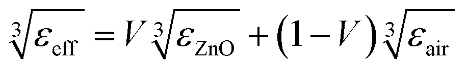
The surface morphologies and the cross-section of the ZnO NWs (length, diameter, and number of NWs per unit area) were examined by using a field-emission scanning electron microscope (FEG-SEM Hitachi SU8030) at an acceleration voltage of 10 kV. Contact angle measurements were conducted using a single water droplet on an OCA 15EC optical contact angle measuring and contour analysis system built by Dataphysics Instruments, Germany. To retrieve large scale porosity in the ZnO NW film, we used the reflection analysis by fitting the interference fringes of the reflection curve with the calculated curve based on the porous thin film model which has been previously reported.28 The reflection spectrum ranging from 350 nm to 830 nm was obtained by placing the sample in an integrating sphere and using a black body white lamp as a light source. The reflected light was recorded by using a spectrometer (SR500i: f = 500 mm, a grating of 84 l mm−1) equipped with an Andor CCD camera. The reflection simulation was based on the transfer matrix method, where the wavelength position and contrast of the fringes in the reflection or transmission curve depends on the thickness and the refractive index of the thin film. The Looyenga model29,30 was applied as an effective medium theory to simulate the porosity by taking into account the cylinder-type shape of the NWs. The effective refractive index can be derived from the effective permittivity, εeff of the NWs thin film which can be expressed as:where εZnO is the permittivity of ZnO, εair is the permittivity of air, and V is the volume fraction of ZnO NWs, respectively. As the thickness of the NWs thin film was known from the SEM images, the large-scale volume fraction can be retrieved by fitting the fringes of the measured reflection curve.
3. Results and discussion
The morphology of ZnO NWs is known to be influenced by many growth parameters such as the growth temperature and time, the concentration22 and the pH value of the growth solution.26 However, there is no report so far, to the best of our knowledge, investigating the influence of substrate size on the morphology of the ZnO NWs grown on it. A time dependent growth study of ZnO NWs on 3-inch wafer was then conducted. The homogeneity of the growth of ZnO NWs was evaluated by verifying the length, volume fraction and the contact angle made by a water droplet on the NWs.3.1 Effect of the substrate size
To investigate the effect of the size of the substrate on the length and total volume of the NWs occupied on the substrate, ZnO NWs were grown on six substrates of different sizes as shown in Table 1 below. For this specific study, 500 mL solution of zinc acetate (35 mM) was used for the growth of the NWs and the total growth time was maintained for an hour.| Number | Surface area (mm2) | Length (nm) | Volume (mm3) |
|---|---|---|---|
| 1 | 271 | 657 ± 75 | 0.18 |
| 2 | 398 | 789 ± 84 | 0.31 |
| 3 | 706 | 648 ± 70 | 0.46 |
| 4 | 944 | 637 ± 64 | 0.60 |
| 5 | 1635 | 559 ± 53 | 0.91 |
| 6 | 6555 | 325 ± 43 | 2.13 |
Table 1 lists the average length and volume of the NWs corresponding to the different substrate sizes. For studying the evolution of the amount of ZnO material actually deposited on the substrate as a function of the substrate size, we can either consider (a) the mass of ZnO which is deposited on the substrate or (b) the effective volume of the ZnO NWs (for which we need to know the porosity of the layer) or (c) the volume of the ZnO NW layer including the spacing between the NWs. These three conditions are only valid if we consider a homogeneous growth of the ZnO NWs on the entire substrate surface. In our case, we decided to use the easiest volume to calculate, the volume of the ZnO NW layer.
As seen from Table 1, it is observed that as the surface size of the substrates increases, the length of the NWs decreases. This is mainly due to the fact that there are a large number of seed grains present on bigger sized substrates as compared to the smaller ones, while the initial concentration of zinc acetate is identical for all the different growths. Thus, the number of Zn2+ ions shared by each NW on bigger size substrates decreases, resulting in NWs with a short length. The volume of the ZnO NWs (considered to be a thin film) was calculated by multiplying the surface area of the substrate with the average length of the NWs. In this case, we assume that the density of the NWs is the same on each sample. We plotted the volume as a function of the substrate size in Fig. 2. It is seen that initially the volume increases linearly with the surface size and begins to saturate when the surface area is larger than 1000 mm2. The linear increase (depicted by a red coloured tangent in Fig. 2 below) shows that the growth speed in the vertical direction is constant for the surface area below 1000 mm2. This suggests that in the first hour, the growth is not limited by the Zn2+ ion concentration. It is worth mentioning that the growth time was kept constant for this study. As for the substrates having a surface size larger than 1000 mm2, the growth speed after an hour of growth is reduced as compared to that of ZnO NWs on a smaller substrate. This is mainly due to the depletion in the amount of Zn2+ ions coming to the sites of the NWs.
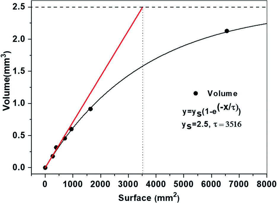 | ||
| Fig. 2 Volume evolution of the ZnO NW layer as a function of the substrate area. The red line is a tangent to the curve at the origin which shows the linear increase of the volume as a function of the surface area i.e. constant length of the NWs. | ||
To be more quantitative, we fitted the experimental data with a curve represented by  where y represents the volume, x represents the surface area, ys is the saturation volume and τ is the characteristic surface constant. The characteristic surface constant τ and the saturation volume ys obtained by fitting the curve are equal to 3516 mm2 and 2.5 mm3, respectively. The saturation volume is highlighted by the dashed line in Fig. 2 above. From this graph one can define 5τ approximately as the surface limit for which no more material is deposited (the growth stops). It is essential to mention that at this value of 5τ, the volume is 99.33% of the limit volume (2.43 mm3). This 5τ surface constant corresponds to almost a 6-inch wafer. For a surface constant larger than τ, one could not expect to grow very long ZnO NWs by further increasing the size of the substrate nor by increasing the growth time further. The growth time will be actually the subject of the next section. To study representatively large surfaces, we use 3-inch wafers. For this wafer size, nevertheless, the surface area (4500 mm2) will be beyond the characteristic surface constant τ (3516 mm2). Yet, if the expected volume of the deposited material will also be representative, we expect to reach the saturation regime for the longer growth time.
3.2 Time dependent growth study
The time dependent growth study on 3-inch silicon wafers was conducted separately in different solutions having the same molar concentration, but varying growth periods. The diameter, length, aspect ratio and number of the NWs were obtained from the SEM images, recorded on the central area of the wafers. The numerical values of these parameters are shown in Fig. 3 below. | ||
| Fig. 3 Time dependent growth of ZnO NWs on a 3-inch silicon wafer: (a) length (black round symbols) and diameter (blue square symbols) of the NWs versus the growth time. Blue and black dashed lines denote the exponential (saturation) fitting curves. Inset shows values of τ and ys obtained after fitting the experimental points. (b) Evolution of the number of NWs as a function of time. Inset shows the SEM image of cross-sectional view of the NWs in which the small NWs are seen to merge with the longer ones. | ||
The length of the NWs is seen to increase quite rapidly in the first 20 min of growth time after which it begins to saturate. The diameter of the NWs is also observed to saturate in the first 15 to 20 min. During the growth of the NWs, there is a simultaneous formation of precipitates occurring in the solution during the heating process.23,26,27 As heating progresses, the nucleation and growth of these precipitates competes for Zn2+ ions which are also involved in the NW growth. At some critical point, the rate of bulk precipitation overtakes the rate of surface deposition, because of the increased probability that Zn2+ ions react on the surface of the precipitate before they can reach the substrate. All this leads to a decrease in the growth rate of the NWs with increasing time up to 80 min.
We fit the evolution of the length and diameter of the NWs as a function of the growth time as done before. Fig. 3(a) shows that the saturation time constant for the length (approx. 14.31 min) of the NWs is longer as compared to the saturation time constant for the diameter (9.43 min) of the NWs. This is mainly due to the fact that probably the lateral growth of NWs is suppressed after a certain time, so the incoming Zn2+ ions are used only for the growth of the NWs in the vertical direction. The fit made to the curve results in a saturation length of 740 nm and a diameter of 50 nm, respectively.
Fig. 3(b) shows the evolution of the number of NWs. The number of NWs is observed to decrease as the time increases. This indicates that the NWs stop growing. This could happen for tilted NWs which will stop growing when they touch the neighbouring wires and most probably start to merge with the neighbouring NWs as the growth time increases. This effect can be seen in the cross-sectional view of the SEM image in the inset of Fig. 3(b) and in Fig. 4.
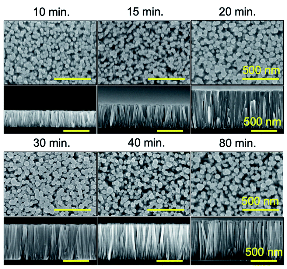 | ||
| Fig. 4 SEM images of top-view and cross-sectional view of the ZnO NWs synthesized on entire 3-inch silicon wafers by CBD. The parameter varied was the growth time. All bars represent 500 nm. | ||
It is worth noting from the cross-sectional SEM images in Fig. 4 that the NWs grown by the CBD technique are highly aligned in the vertical direction. There are a very few NWs which appear to be tilted. The error bars shown in the graphs in Fig. 3(a and b) correspond to the standard deviation of the values obtained for the length, diameter and number of NWs. These measurements were conducted for a large number of NWs (40) on the same sample.
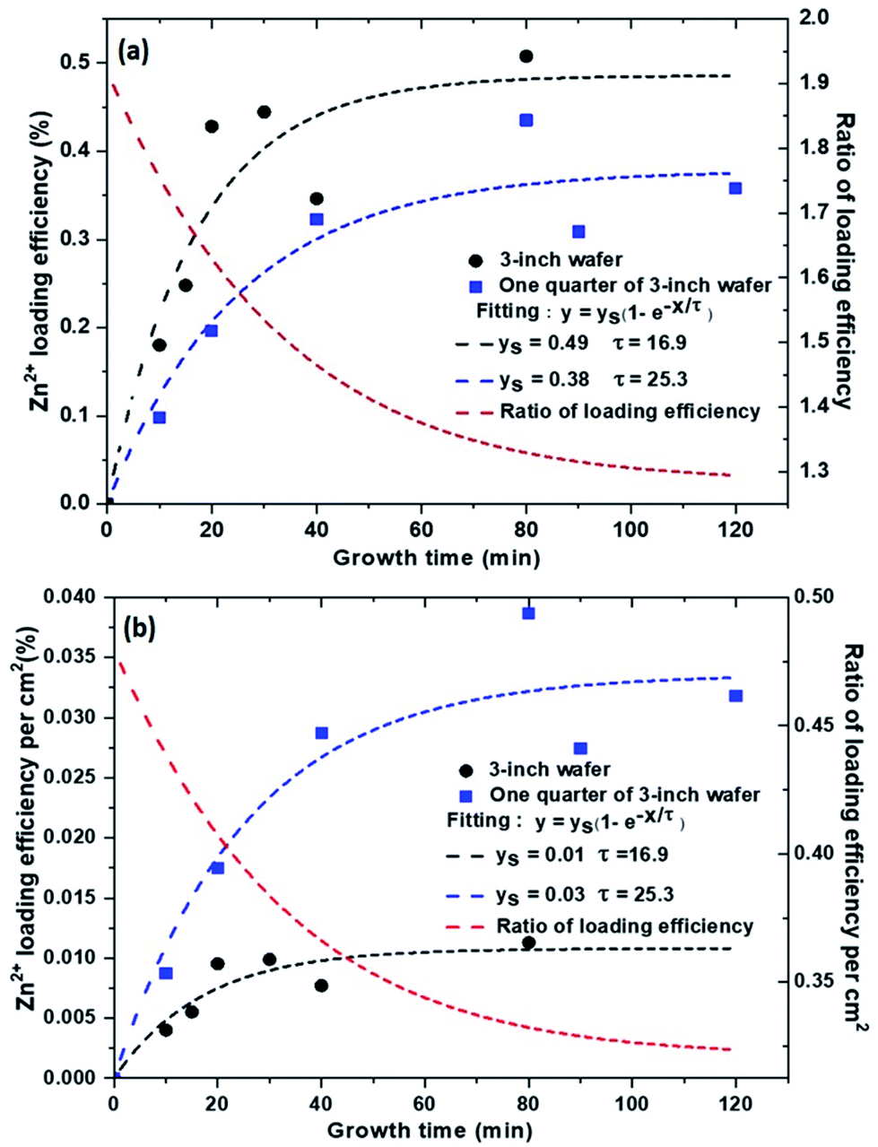
3.3 Loading efficiency
The proportion of Zn2+ which contributes to the ZnO NW growth is obtained by weighing the sample before and after the growth. The loading efficiency of Zn2+ ions can be calculated by dividing the moles of the deposited ZnO by the moles of the initially added Zn2+ ions in the nutrient solution.Fig. 5(a) above shows the values of the loading efficiencies of the samples obtained from the time dependent growth studies on a full 3-inch silicon wafer (black symbols and black dashed curve) and a quarter of a 3-inch silicon wafer (blue symbols and blue dashed curve). The growth time was varied from 10 min to 120 min. The overall values (<1%) indicate that only a very small proportion of the added ions have contributed to the growth of the NWs. These relatively small values can be explained by the fact that during the growth process, apart from the growth of NWs, there are also ZnO micropods which are forming freely in the solution. SEM images of these micropods are shown in Fig. S2.† The amount (mass) of the micropods formed is quite large as compared to the amount of the ZnO NWs. This further confirms that a large number of Zn2+ ions are involved in the formation of the micropods in solution as compared to the ZnO NWs. This micropod formation thereby reduces the number of Zn2+ ions in the solution which would be available for the formation of the ZnO NWs. This direct precipitation which is a limiting factor explains the low loading efficiency reported here (cf. ESI† for further discussion).
 | ||
| Fig. 5 Evolution of the growth time dependent Zn2+ ion loading efficiency: (a) curves showing the loading efficiencies for growth conducted on full 3-inch substrates and a quarter of a 3-inch substrate. Black and blue dashed lines denote the exponential fitting curves while the red line denotes a ratio of the two loading efficiencies. (b) Curves (blue and black dashed lines) showing the loading efficiency per cm2 for the 3-inch substrate and a quarter of a 3-inch substrate while the red line denotes a ratio of the two loading efficiencies per cm2. | ||
If we now consider the effect of the surface area on the loading efficiency, it is interesting to see that the 3-inch wafer shows higher loading efficiency of ions at any given time as compared to the quarter of a 3-inch silicon wafer (Fig. 5). For the 3-inch silicon wafer, the growth time of the NWs was varied only till 80 min and not beyond, as the growth had already reached its maximum limit in 80 min.
By fitting the experimental points with a saturation curve, we obtained a saturation time constant of 16.9 min for ZnO NWs grown on a 3-inch wafer whereas the saturation time constant for the ZnO NWs grown on a quarter of a 3-inch wafer is longer, nearly 25.3 min. It should be mentioned here that, we conducted two more experiments for a longer growth time in the case of a quarter size substrate for observing a clear saturation tendency.
The red dashed curve in Fig. 5(a) shows the evolution of the ratio of the two fitted curves. The decrease in the ratio indicates that the growth speed for the large substrate decreases faster as compared to the smaller substrate. The curve saturates at a value about 1.29 approximately, which, in turn, confirms that by increasing the substrate area, we improved the ion loading efficiency.
Further, we also calculated the ion loading efficiency per cm2. This efficiency calculated per cm2 of the surface area also involves the kinetics of NWs growth because here we can state that this study tends to compare the same surface size in both the samples. As seen in Fig. 5(b) above, one quarter of a 3-inch wafer shows a higher loading efficiency per cm2 as compared to an entire 3-inch silicon wafer, contrary to what is expected. This observation complements the results obtained in Section 3.1, Table 1 wherein it has been proved that for a small surface size, the length of NWs is longer implying that the loading efficiency per cm2 is higher. The ratio of the loading efficiency (red curve) in Fig. 5(b) is much lower (0.33) in comparison to the ratio of the loading efficiency (red curve) in Fig. 5(a) which is greater than 1. This is due to the fact that the effective surface area under consideration is much larger in Fig. 5(a) as compared to Fig. 5(b). Thus overall, it is proved that the surface area plays a major role on the controllable growth of NWs.
3.4 Well-aligned growth of ZnO NWs on an entire wafer
After growing the ZnO NWs on a 3-inch silicon wafer, we have evaluated the thickness, volume fraction and contact angle at different positions on the sample. Fig. 6(a) above shows a photograph of the 3-inch ZnO NWs sample grown for 40 min. It is to be noted that the solution was not stirred during the growth of the NWs in order to have a well-aligned ZnO NW layer. If the stirring is known to avoid the increase in the ion concentration locally, it might also make the micropods float in the solution, which can lead to inhomogeneous deposition on the ZnO NWs.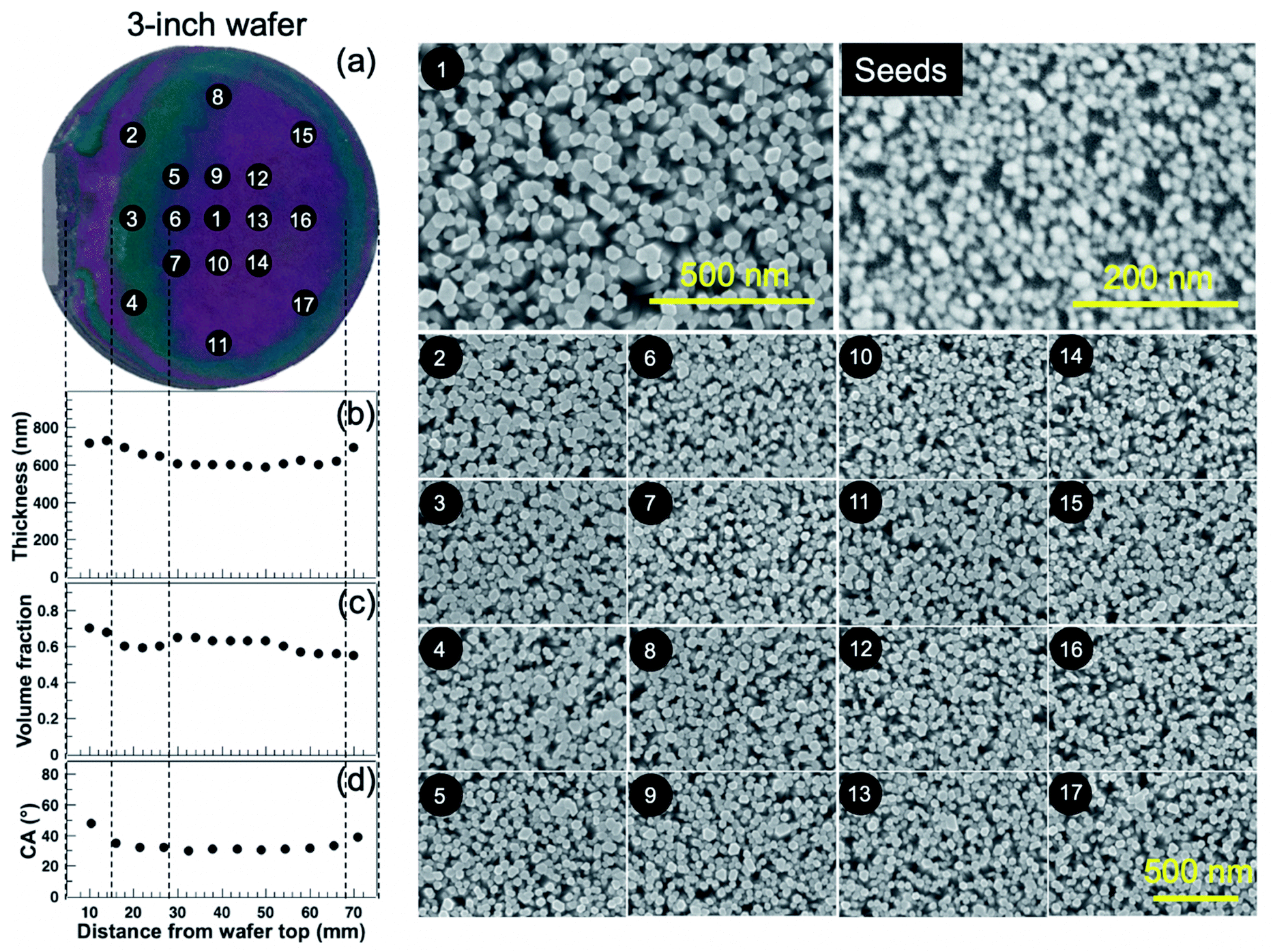 | ||
| Fig. 6 Homogeneity of the ZnO NWs on the 3-inch silicon wafer grown for 40 minutes: (a) photograph of the entire wafer after growth of ZnO NWs. The portion on the left-hand side of the wafer which does not have any growth of ZnO NWs is the top part, and the area near points 15, 16 and 17 is the bottom part of the wafer. Evolution of the thickness (b), volume fraction (c) and contact angle (CA) (d) as a function of the distance from the left edge of the wafer. The top right-hand side SEM image corresponds to the seed layer used for the growth of the NWs. The remaining SEM images are the top view of the NWs taken at different positions on the silicon wafer, while the number on the image corresponds to the number marked in the photograph. | ||
The coloured fringe patterns on the sample arise from the interferences occurring between the top and bottom interfaces of the thin films i.e. air/ZnO and ZnO/substrate interfaces. These colour differences arise due to the difference in the length and potentially also the density of the ZnO NWs. Previous studies have reported that the fringe-like patterns correspond to the temperature profile of the solution.31 In our CBD system too, there is a thermal gradient which exists in the solution during the growth of the ZnO NWs. This thermal gradient may be avoided if the solution is stirred. Since the sample in our case is vertically placed in the flask, the lower part of the sample is heated more as compared to the top portion near the lid of the system. Even if the effect is clearly visible because of the interference nature of the colour, it only gives rise to a NW height difference of about 5.7% (±37 nm).
The round circular strip present all along the border of the silicon wafer is due to the spin coating process of the seed layer wherein the seed solution accumulates at the edge of the wafer resulting in more seed grains that will result in NWs having a larger dimension. This can be overcome by using a dip-coating technique which is known to better prevent the edge effect and lead to higher homogeneous surface coverage. As shown in Fig. 6(b) the difference in length or the thickness of the NWs between the green and red coloured area shows a variation of about 5.7% which is not large. The length of the NWs measured at different positions in the red coloured area are quite similar, approximately 605 nm (having a variation of ±3%) and having a diameter of about 50 nm, approximately. The difference in length of the NWs measured in the various areas in the green region only corresponds to ±1% which is extremely low. Here, we consider the well-aligned NWs to be a film having a certain thickness.
In addition, Fig. 6(c) shows the simulated densities of the NWs, at different areas which are quite uniform in the same colour range. In Fig. 6(d), the results of the contact angle measurements show that the ZnO NWs are hydrophilic in nature having a contact angle of about 30°, except at the border where the contact angle is measured to be around 40°. At a distance 10 mm from the flat edge of the silicon wafer, the ZnO NWs have a larger volume fraction (volume fraction is the ratio of real volume of ZnO divided by the volume of ZnO with pores included) as their length and diameter is slightly larger as compared to the other areas. An increase in the volume fraction of the NWs implies that the porosity between the NWs has decreased. This will result in less water penetrating in the pores between the NWs as the air inside these pores will act as a cushion (Cassie–Baxter regime). Hence, we will obtain a slightly higher contact angle as compared to the NWs in the other regions.
Fig. 6 depicts the SEM images of the top-view of the NWs from different areas (from point 1 to point 17), grown on a 3-inch silicon wafer. The distribution and the size of the NWs appear to be quite uniform within the same colour range of the sample.
3.5 Towards batch production
After growing highly crystalline ZnO NWs on a 3-inch silicon wafer, simultaneous growth of ZnO NWs was conducted on two 4-inch silicon wafers placed vertically back to back in the solution. The seed layer coated sides on the two wafers were exposed to the solution while the uncoated sides of the wafers were placed back to back. Fig. 7 above shows the photograph of the two 4-inch silicon wafers after the growth of ZnO NWs for a time period of one hour. Similar colored interference fringes are observed on both the samples which further proves that the ZnO NWs grown simultaneously on the two large wafers are highly comparable. This proves that it is possible to do a batch production of ZnO NWs on several wafers at the same time.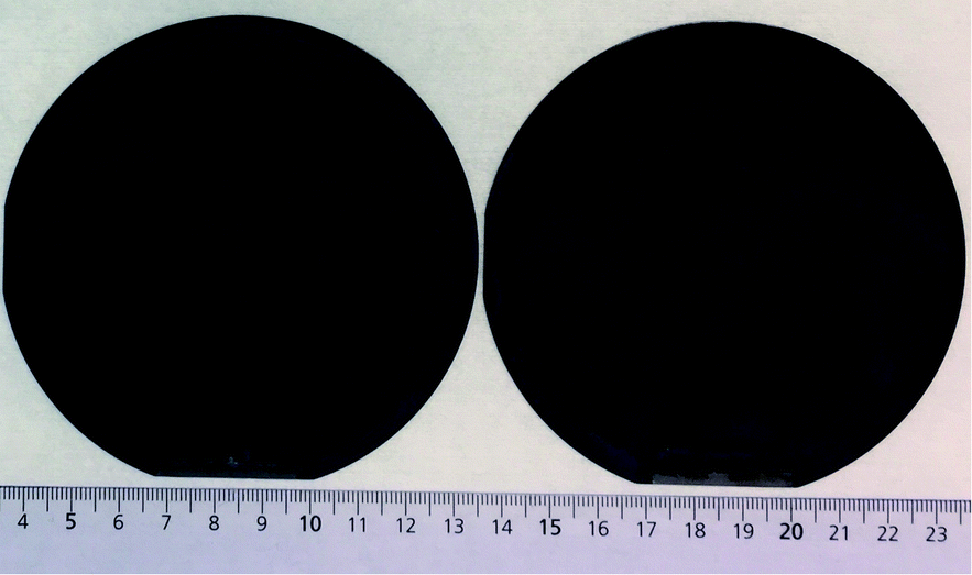 | ||
| Fig. 7 ZnO NWs grown on two 4-inch silicon wafers simultaneously. | ||
4. Conclusions
In this work, we investigated using the chemical bath deposition technique, the wafer scale growth of ZnO NWs and the limiting factors involved therein. We have successfully grown well-aligned ZnO NWs on entire 3-inch or 4-inch silicon substrates. A quantitative study on the substrate size dependent growth proved that as the surface size of the substrates increased, the length of the NWs decreased. The volume of ZnO was observed to increase almost linearly with the surface size and began to saturate when the surface area was larger than 1000 mm2. Overall, it was observed that the growth of the NWs on a 3-inch wafer is influenced by the depletion of the Zn2+ ions in the solution.The time dependent growth study of ZnO NWs conducted on entire 3-inch wafers proved that the length and the diameter of the NWs increased rapidly in the first 15–20 min of growth time after which it began to saturate. This was mainly attributed to the simultaneous free formation of ZnO microstructures in the solution which compete with the Zn2+ ions that are responsible for the NW growth. The best fit evolution of the length and diameter of the NWs as a function of growth time showed that the saturation time constant for the length (approx. 14.31 min) was longer as compared to the saturation time constant for the diameter, i.e. 9.43 min. This is mainly due to the fact that probably the lateral growth of NWs is suppressed after a certain time, so the incoming Zn2+ ions are used only for the growth of the NWs in the vertical direction. A comparative, quantitative study of the loading efficiency of zinc ions was conducted on an entire 3-inch silicon wafer and a quarter of a 3-inch wafer. The results showed that we could increase the loading efficiency by 1.3 times merely by increasing the substrate surface area from a quarter to a full-size wafer. It is also important to note that the study conducted on the Zn2+ ion loading efficiency per cm2 of surface was found to be higher than in the case of small surfaces. Nevertheless, the loading efficiency remains low (less than 1%) and constitutes one of the major perspectives of this work. Uniformity of the growth on the entire 3-inch wafers was also confirmed by the length, volume fraction and contact angle measurements. To conclude, well-aligned and batch compatible growth of ZnO NWs on two 4-inch wafers is easily obtained, which can facilitate the future large-scale applications of ZnO NWs arrays in solar cells, light emission and biomedical devices for high-throughput diagnostics.
Conflicts of interest
There are no conflicts to declare.Acknowledgements
The authors would like to thank Dr Pierre Le Barny for all his useful comments and discussion and the Nanomat platform for the use of equipment. Dr Zhou would like to thank China Scholarship Council for his PhD fellowship (no. 201306120067).References
- M. Wilander, Zinc Oxide Nanostructures: Advances and Applications, Pan Stanford, New York, 2013 Search PubMed.
- T. Cossuet, J. Resende, L. Rapenne, O. Chaix-Pluchery, C. Jiménez, G. Renou, A. J. Pearson, R. L. Z. Hoye, D. Blanc-Pelissier, N. Duy Nguyen, E. Appert, D. Muñoz-Rojas, V. Consonni and J.-L. Deschanvres, Adv. Funct. Mater., 2018, 28, 1803142 CrossRef.
- M. Zhang, E. Stefanakos and D. Goswami, J. Nanomater., 2012, 2012, 1–22 Search PubMed.
- R. C. W. Rolf Könenkamp and C. Schlegel, Appl. Phys. Lett., 2004, 85, 6004–6006 CrossRef.
- H. Jeong, D. Park, H. Leem, Y. Ko, J. Yu, S. Choi, D. Lee, E. Suh and M. Jeong, Nanoscale, 2014, 6, 4371–4378 RSC.
- H. Huang, S. Mao, H. Feick, H. Yan, Y. Wu, H. Kind, E. Weber, R. Russo and P. Yang, Science, 2001, 292, 1897–1899 CrossRef.
- R. Aad, V. Simic, L. Le Cunff, L. Rocha, C. Sartel, V. Sallet, A. Lusson, C. Couteau and G. Lerondel, Nanoscale, 2013, 5, 9176–9180 RSC.
- V. Consonni, J. Briscoe, E. Kärber, X. Li and T. Cossuet, Nanotechnology, 2019, 30, 362001 CrossRef CAS.
- Z. Wang, J. Phys.: Condens. Matter, 2014, 16, R829–R858 CrossRef.
- H. Chen, C. Chen, Y. Chang, C. Tsai, R. Liu, S. Hu, W. Chang and K. Chen, Angew. Chem., Int. Ed., 2010, 49, 5966–5969 CrossRef CAS.
- A. Wolcott, T. R. Kuykendall, W. S. Chen, W. Chen and J. Z. Zhang, J. Phys. Chem. B, 2006, 110, 25288–25296 CrossRef CAS.
- I. Azzouz, Y. Ghozlane Habba, M. Capochichi-Gnambodoe, F. Marty, J. Vial, Y. Leprince-Wang and T. Bourouina, Microsyst. Nanoeng., 2018, 4, 17093–17100 CrossRef CAS.
- M. Zhang, T. An, X. Liu, X. Hu, G. Sheng and J. Fu, Mater. Lett., 2010, 64, 1883–1886 CrossRef CAS.
- J. Qu, C. Luo and Q. Cong, Nano-Micro Lett., 2011, 3, 115–120 CrossRef CAS.
- H. Chen, X. Wu, L. Gong, C. Ye, F. Qu and G. Shen, Nanoscale Res. Lett., 2010, 5, 570–575 CrossRef CAS.
- Y. C. Kong, D. P. Yu, B. Zhang, W. Fang and S. Q. Feng, Appl. Phys. Lett., 2001, 78, 407–410 CrossRef CAS.
- G. Zhu, R. Yang, S. Wang and Z. L. Wang, Nano Lett., 2010, 10, 3151–3155 CrossRef CAS.
- T. Pauporté, E. Jouanno, F. Pellé, B. Viana and P. Aschehoug, J. Phys. Chem. C, 2009, 113, 10422–10431 CrossRef.
- O. Lupan, V. Guérin, I. Tiginyanu, V. Ursaki, L. Chow, H. Heinrich and T. Pauporté, J. Photochem. Photobiol., A, 2010, 211, 65–73 CrossRef CAS.
- A. Mute, M. Peres, T. Peiris, A. Lourenço, L. Jensen and T. Monteiro, J. Nanosci. Nanotechnol., 2010, 1, 2669–2673 CrossRef.
- A. Gokarna, J. H. Kim, F. Leroy, G. Patriarche, P. Roussel, Z. Bougrioua, C. Rodriguez, E. Dogheche and Y.-H. Cho, J. Lumin., 2013, 144, 234–240 CrossRef CAS.
- A. Gokarna, R. Parize, H. Kadiri, K. Nomenyo, G. Patriarche, P. Miska and G. Lerondel, RSC Adv., 2014, 4, 47234–47239 RSC.
- A. Gokarna, R. Aad, J. Zhou, K. Nomenyo, A. Lusson, P. Miska and G. Lerondel, J. Appl. Phys., 2019, 126, 1–11 CrossRef.
- L. E. Greene, M. Law, J. Goldberger, F. Kim, J. C. Johnson, Y. Zhang, R. J. Saykally and P. Yang, Angew. Chem., Int. Ed. Engl., 2003, 42, 3031–3034 CrossRef CAS.
- M. Erfan, M. Gnambodoe-Capochichi, F. Marty, Y. M. Sabry, T. Bourouina and Y. Leprince-Wang, Nanoscale, 2020, 12, 1397–1405 RSC.
- B. Cao and W. Cai, J. Phys. Chem. C, 2008, 112, 680–885 CrossRef CAS.
- R. Parize, J. Garnier, O. Chaix-Pluchery, C. Verrier, E. Appert and V. Consonni, J. Phys. Chem. C, 2016, 120, 5242–5250 CrossRef CAS.
- J. Zhou, L. O. Le Cunff, K. Nomenyo, A. Vial, T. Pauporté and G. Lerondel, Thin Solid Films, 2019, 675, 43–49 CrossRef CAS.
- L. Landau and E. Lifshitz, Course of Theoretical Physics, Pergamon Press, New York, 2nd edn, 1982, vol. 8 Search PubMed.
- H. Looyenga, Physica, 1965, 31, 401–406 CrossRef CAS.
- K. M. McPeak and J. B. Baxter, Ind. Eng. Chem. Res., 2009, 48, 5954–5961 CrossRef CAS.
Footnotes |
| † Electronic supplementary information (ESI) available. See DOI: 10.1039/d0na00434k |
| ‡ These authors contributed equally to this work. |
| § These authors were leading the project. |
| This journal is © The Royal Society of Chemistry 2020 |