
 Open Access Article
 This Open Access Article is licensed under a Creative Commons Attribution-Non Commercial 3.0 Unported Licence
In situ monitoring of electrical and optoelectronic properties of suspended graphene ribbons during laser-induced morphological changes†
Xiaosi
Zhang
a,
Thayer S.
Walmsley
b and
Ya-Qiong
Xu
 *ab
*ab
aDepartment of Electrical Engineering and Computer Science, Vanderbilt University, Nashville, TN 37235, USA. E-mail: yaqiong.xu@vanderbilt.edu
bDepartment of Physics and Astronomy, Vanderbilt University, Nashville, TN 37235, USA
First published on 17th July 2020
Abstract
Exploring ways to tune and improve the performance of graphene is of paramount importance in creating functional graphene-based electronic and optoelectronic devices. Recent advancements have shown that altering the morphology of graphene can have a pronounced effect on its properties. Here, we present a practical and facile method to manipulate the morphology of a suspended graphene ribbon using a laser to locally induce heating while monitoring its electrical and optoelectronic properties in situ. Electrical measurements reveal that the conductance of suspended graphene transistors can be tuned by modifying its morphology. Additionally, scanning photocurrent measurements show that laser-induced folded graphene ribbons display significantly enhanced localized photocurrent responses in comparison with their flat counterparts. Moreover, the localization of the laser-induced heating allows for a series of folds to be induced along the entire graphene ribbon, creating targeted photocurrent enhancement. Through further investigations, it is revealed that the photo-thermoelectric effect is the primary mechanism for the increased photocurrent response of the device. Our experimental results explore the mechanisms and consequences of the folding process as well as provide a strategy to manipulate morphology and physical properties of graphene for future engineering of electronics and optoelectronics.
Introduction
Two-dimensional (2D) materials, including graphene, transition metal dichalcogenides (TMDs), and hexagonal boron nitride (h-BN) have triggered extensive research due to their novel mechanical, optical, and electrical properties as well as their successful applications in electronic and optoelectronic devices such as field-effect transistors, integrated circuits, photodetectors, solar cells, light-emitting diodes, and lasers.1–5 Graphene has become one of the most promising materials for photodetection and photovoltaics due to its ultrahigh charge-carrier mobility and broadband absorbance in the near-infrared and visible spectral ranges.6,7 However, graphene's semi-metallic nature and associated zero bandgap have greatly limited its implementation in electronic and optoelectronic applications. Despite the majority of graphene research focusing on planar geometry properties, several theoretical and experimental studies show that folds in graphene's structure alter its electrical and optical properties to overcome some of these limitations and enhance the performance of graphene-based devices.8–10 Theoretically, molecular dynamics (MD) simulations predict that the twisting graphene nanoribbon structure would lead to a tunable modification of the electrical properties of graphene.11,12 Experimentally, suspended graphene sheets have been shown to fold under powerful ultrasonic stimulations13 or by the introduction of anisotropic surface curvature during graphene synthesis or the transfer process.14 It has also been demonstrated that a scanning tunneling microscope (STM) tip can be used to induce the folding and unfolding of the graphene membrane along a specific direction resulting in altered electrical properties.15 In addition to these methods, other ways have been explored to change graphene's morphology but keep its original electrical properties such as in kirigami-inspired manual folding of pre-patterned graphene ribbons to build mechanical metamaterials such as stretchable electrodes, springs, and hinges.16 Despite these advancements, there appears to be no facile method that can simultaneously alter the morphology of graphene while monitoring the associated changes in the electrical and optoelectronic properties in a tunable and variable fashion. It is necessary to demonstrate a platform that enables to change the graphene morphology in situ, which allows the study of underlying physical mechanisms as well as novel engineering approaches to tune the electrical and optoelectronic properties of graphene. Such a unique tuning approach could have profound implications and may open the door for next-generation graphene-based photodetection and photovoltaics.In this paper, we report a practical and versatile method to manipulate graphene's electrical and optoelectronic properties by locally modifying the morphology of a suspended graphene ribbon via a laser beam. We compare the conductance and photoresponse of flat graphene ribbons with those possessing various degrees of folded structures, suggesting that the electrical properties can be tuned and the photocurrent can be locally enhanced. An increase of 12.9% in the conductance of graphene ribbons is observed, followed by a decrease of 36%. This is likely attributed to the nature of the folding process, which can be triggered when the local temperature increases to 600 K via a laser beam. Furthermore, the spatial control over the photocurrent enhancement was also demonstrated by employing local laser-induced heating. Further studies reveal that the enhanced photocurrent responses of the folded graphene structures are mainly attributed to the photo-thermoelectric effect (PTE). These experimental results provide a facile method to alter the morphology of graphene as an effective approach to manipulate its electrical and optoelectronic properties.
Materials and methods
Graphene synthesis and device fabrication
Graphene was synthesized through a standard chemical vapor deposition (CVD) method.17–19 Graphene was grown on copper foil at 1000 °C in the presence of 20 sccm of methane and 80 sccm of hydrogen for 30 minutes. Then the as-grown graphene was transferred onto a 170 μm thick coverslip with pre-patterned Ti/Au electrodes using the bubbling transfer technique.20 Here, the drain and source electrodes were patterned via standard photolithography, followed by a deposition of 5 nm of Ti and 40 nm of Au through e-beam deposition. Next a 2 μm-wide graphene ribbon was defined using a standard photolithography and etching process. The graphene ribbon device was then sealed into a microfluidic chamber, which was formed by placing a piece of patterned parafilm between the blank coverslip and the one with the graphene ribbon.21 After that, the graphene ribbon was suspended across an 11 μm wide and 2 μm deep trench by a buffered oxide etchant (BOE) wet etching process. This wet etching process doesn't significantly impact the quality of the graphene ribbon nor induce significant strain as confirmed by Raman spectroscopy measurements provided in the supplemental materials (Fig. S1†).22–24 Deionized water was then used to flush the device to remove all BOE residues. Finally, the cleaned chamber was filled with a 1× phosphate-buffered saline (PBS) solution and a third gold electrode was used as an electrolyte-gate to change the electrochemical potential, creating an electrolyte gated field-effect transistor (EGFET).Experimental
Two laser systems were used in this experiment. The first system consists of a high power 1064 nm laser which was applied to alter the morphology of graphene. The laser was ported into an inverted microscope and focused onto a graphene ribbon with a diffraction-limited laser spot (<1 μm) by using a 60× water immersion Olympus objective with NA = 1.2. To tune the laser power, a continuously variable ND filter controlled by a mechanical stage was placed in the optical path. The second 785 nm continuous-wave laser system was employed to perform scanning photocurrent microscopy to monitor the photoresponse of the suspended graphene ribbon. The laser beam was transmitted through the transparent substrate to scan over the entire suspended graphene device using piezo-controlled mirrors with nanometer-scale spatial resolution. Photocurrent signals were collected via a current preamplifier and the corresponding reflection image was recorded through a silicon photodetector.Results and discussion
Fig. 1a shows the schematic diagram of a typical graphene transistor. The suspended graphene ribbon exhibits an ambipolar behavior with the Dirac point close to 1.57 V (Fig. 1b), suggesting p-type characteristics at a zero gate voltage.25,26 In order to manipulate and monitor the optoelectronic properties of the suspended graphene, two lasers were used in this experiment (details provided in Materials and methods). Electrical and optoelectronic properties were examined before altering the morphology of the suspended graphene ribbon. Fig. 1c displays the conductance measurement of the flat graphene ribbon (black line). The optical and photocurrent images of the flat graphene ribbon are shown in Fig. 2a and b, respectively. The photocurrent response for a suspended flat graphene ribbon is less than 1 nA under a zero drain-source bias and a zero gate voltage. Here the photocurrent signals at metal–graphene junctions originate from the Schottky-like barriers formed between the graphene ribbon and metal electrodes, leading to built-in electric fields in these regions to efficiently separate photo-excited electron–hole pairs and thus to generate currents.27 The photocurrent response along the suspended graphene ribbon may result from the chemical residues created during the fabrication process.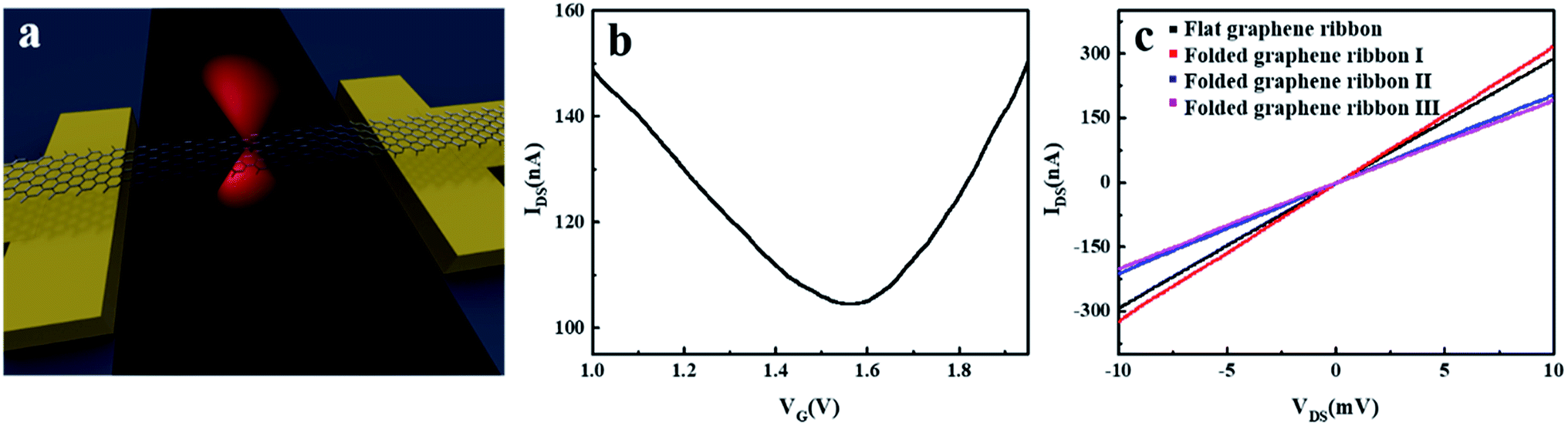 | ||
| Fig. 1 (a) Schematic diagram of our experimental setup showing a laser beam focused on a flat monolayer graphene ribbon suspended across a trench to locally change the morphology of the graphene ribbon. Drain-source electrodes are used to apply a voltage across the suspended graphene ribbon and the third electrode was used as an electrolyte gate. (b) Gate-dependent transport characteristics of a suspended flat graphene transistor. (c) The linear output characteristics of the graphene ribbon with different morphologies (VG = 0 and VDS = 10 mV). | ||
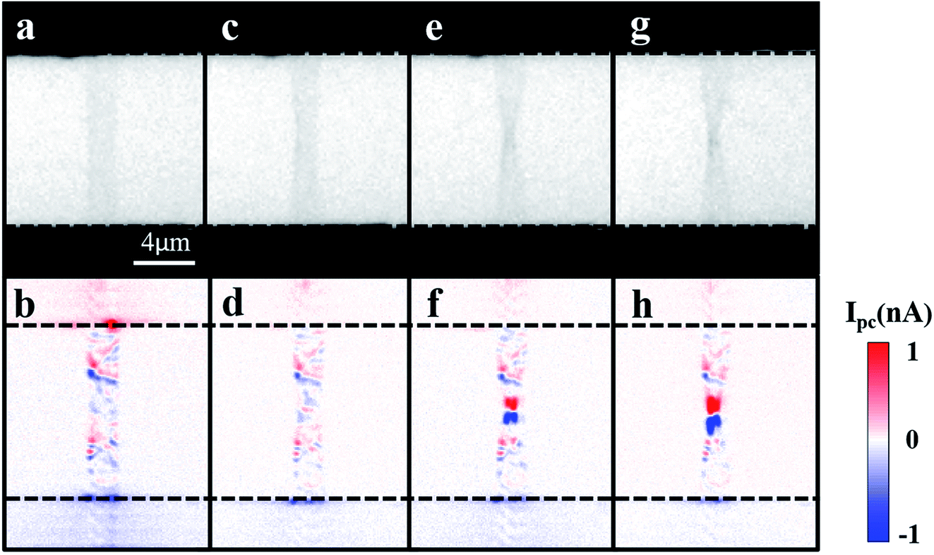 | ||
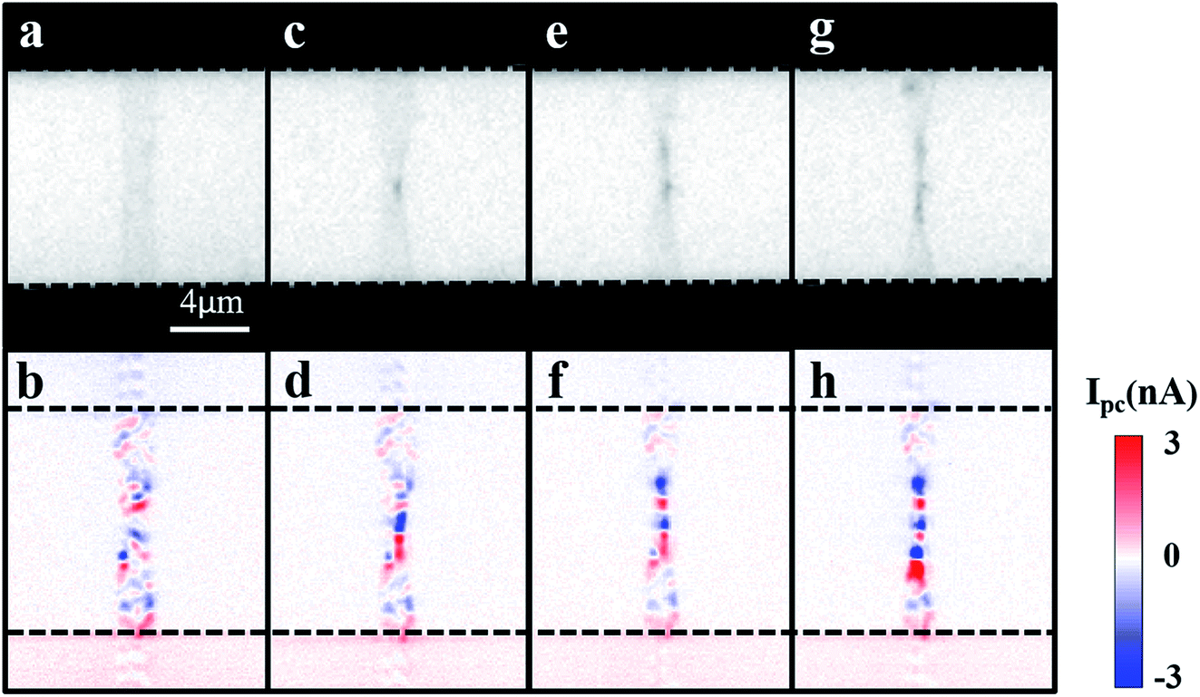
| Fig. 2 (a) Optical and (b) photocurrent images of the suspended flat graphene ribbon. (c) Optical and (d) photocurrent images of the folded graphene ribbon I. (e) Optical and (f) photocurrent images of the folded graphene ribbon II. (g) Optical and (h) photocurrent images of the folded graphene ribbon III. The trench edges are marked by the black dashed-lines. | ||
Once the initial properties were assessed, the graphene morphology was altered by a focused 1064 nm laser beam. At the same time, the conductance of the graphene ribbon was recorded under a 10 mV drain-source bias when the laser power gradually increases. Initially the current slowly increased, owing to photocurrent generation.6 When the laser power was above 46 mW, an abrupt change in the total conductance was observed, likely resulting from the laser-induced morphology change (folded graphene ribbon I). As shown in Fig. 2c, the center of the graphene ribbon, where the 1064 nm laser was focused, was slightly folded, which was further evidenced by the associated change in Raman spectroscopy measurements (Fig. S2†). The related photocurrent image also confirmed that there was a relatively narrow central region in the folded graphene ribbon I (Fig. 2d). Moreover, the I–V characteristics imply that the conductance of the folded graphene ribbon device (red line in Fig. 1c) increased in comparison with the flat graphene counterpart, which is likely attributed to the formation of a multilayer graphene structure. When the graphene ribbon forms a folded structure, additional layers can move to cover the voids and cracked areas of the original monolayer graphene, resulting in the increased conductance of the suspended graphene ribbon.28,29
When we continued to expose this suspended graphene ribbon to the 1064 nm laser at the same focused position for 150 seconds, the center of the graphene ribbon was further folded as shown in Fig. 2e (folded graphene ribbon II), where the width of the suspended graphene ribbon in the center region was further reduced. Interestingly, the conductance of the graphene ribbon decreased (blue line in Fig. 1c). Here the deeply-folded graphene ribbon may form crease regions with tubular nanostructures on the edge in random directions, which can act as tunnel barriers to block the current flow and thus to reduce the conductance of the device.15,30,31 We have also found that a further deeply-folded process (another 150 second laser exposure, folded graphene ribbon III, Fig. 2g) cannot significantly change the device conductance (magenta line in Fig. 1c). However, the deeply-folded process can induce substantially strong photocurrent signals in the deeply-folded region of the graphene ribbon (Fig. 2h). Our studies suggest that a focused laser beam can be utilized to manipulate the conductance and photocurrent response of a graphene ribbon.
To further understand this folding mechanisms, we estimate the local temperature distribution along the suspended graphene ribbon. When the laser beam is focused on the center of the suspended graphene ribbon the laser beam can locally heat carbon atoms to provide energies for a local folding process as predicted by MD simulations.32 The temperature distribution along the graphene ribbon can be obtained from the following heat diffusion equation in the cylindrical coordinate:33–35
 | (1) |
 is laser-induced local heat, q0 is the peak absorbed laser power per unit area at the center of the beam spot,
 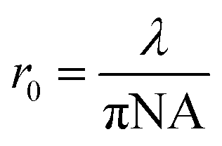 is the radius of the Gaussian laser spot, NA is the numerical aperture. The total absorbed laser power is given by P = q0πr02, which can be estimated by our trigger power (46 mW) and the optical absorption of graphene (2.3%).37 By using the boundary conditions of
 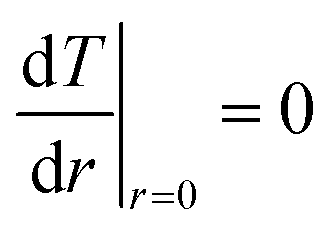 and ΔT|r=∞ = 0, we can calculate the temperature distribution along the graphene ribbon:
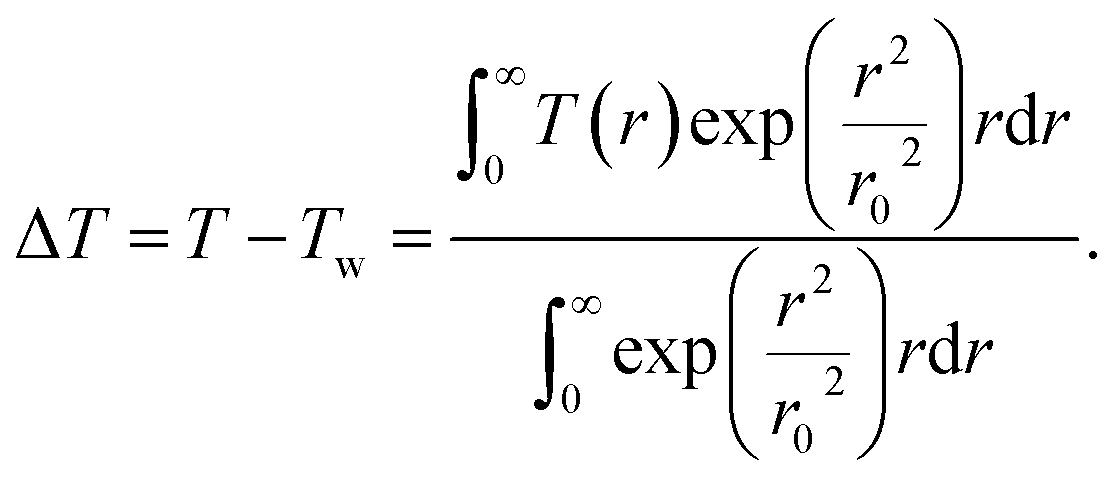 | (2) |
The calculated temperature rise (ΔT) in the radius of the 1064 nm Gaussian laser spot area is ∼300 K, which is expected to provide sufficient energies for carbon atoms to generate the necessary random momenta to induce the folds in the graphene ribbon as predicted by the aforementioned MD simulations.32
In addition, we can further enhance the photocurrent response of an entire graphene ribbon by generating a series of locally-folded structures along it. The evolution of this process is shown in Fig. 3a–h. To begin the folding process, the 1064 nm laser was first focused on the center of the suspended flat graphene ribbon (Fig. 3c and d), then moved up by a step of 1 μm relative to center (Fig. 3e and f), and finally moved down by a step of 1 μm relative to center (Fig. 3g and h). As we expected, the laser beam could create a series of folded-structures and thus strong photocurrent signals along the graphene ribbon. Here we provide a facile way to locally manipulate photocurrent responses in a graphene ribbon.
 | ||
| Fig. 3 (a), (c), (e) and (g) are the optical images of the graphene ribbon. (b), (d), (f) and (h) are the corresponding photocurrent images. The laser power was 0.5 mW for all photocurrent images. The trench edges are marked by the black dashed-lines. | ||
Furthermore, we performed gate-dependent scanning photocurrent measurements to investigate the photocurrent generation mechanisms present in these folded graphene structures. Fig. 4a and b show the optical and photocurrent images of a folded graphene ribbon, respectively, in which the monolayer region of the graphene is maintained between the folded region and the electrodes. By scanning the laser along the gray dashed-line in Fig. 4b while sweeping the gate voltage from 1.5 V to 2.2 V, we obtained the gate-dependent scanning photocurrent map (Fig. 4c). The photovoltage established across the device can be determined from Vpc = IpcR, where Ipc is the linecut across the green dashed-line in Fig. 4c and R is the gate-dependent resistance obtained from the electrical transport measurements (Fig. 4f). As shown in Fig. 4d, Vpc exhibits strong nonmonotonic gate-dependence, which is likely related to the photo-thermoelectric effect (PTE). Because the Seebeck coefficients (S) in different regions of a folded graphene ribbon are expected to be different, the photovoltage due to the PTE can be formulated as VPTE = ΔSΔT. According to the Mott relation,38 we can derive the Seebeck coefficient as
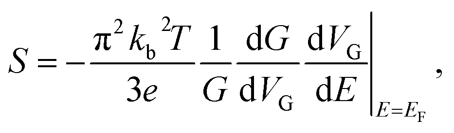 | (3) |
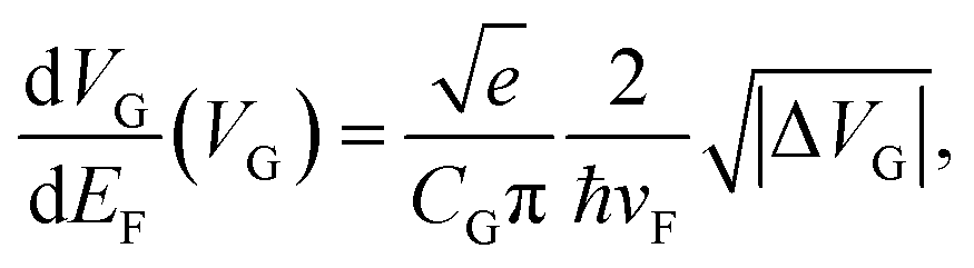 where ΔVG = VG − VDirac, ℏ is the Plank's constant, the vF is the Fermi velocity and CG is the gate capacitance.40 The calculated Seebeck coefficient as a function of gate voltage is shown in Fig. 4e. It is obvious that Vpc has a nearly similar gate-dependent pattern to the calculated Seebeck coefficient, suggesting that photocurrent signals in folded structures are mainly attributed to the PTE.41,42 Recently PTE-induced photocurrent responses have also been observed at single-bilayer graphene junctions and TMDC-metal junctions due to the Seebeck coefficient difference across these junctions.43,44
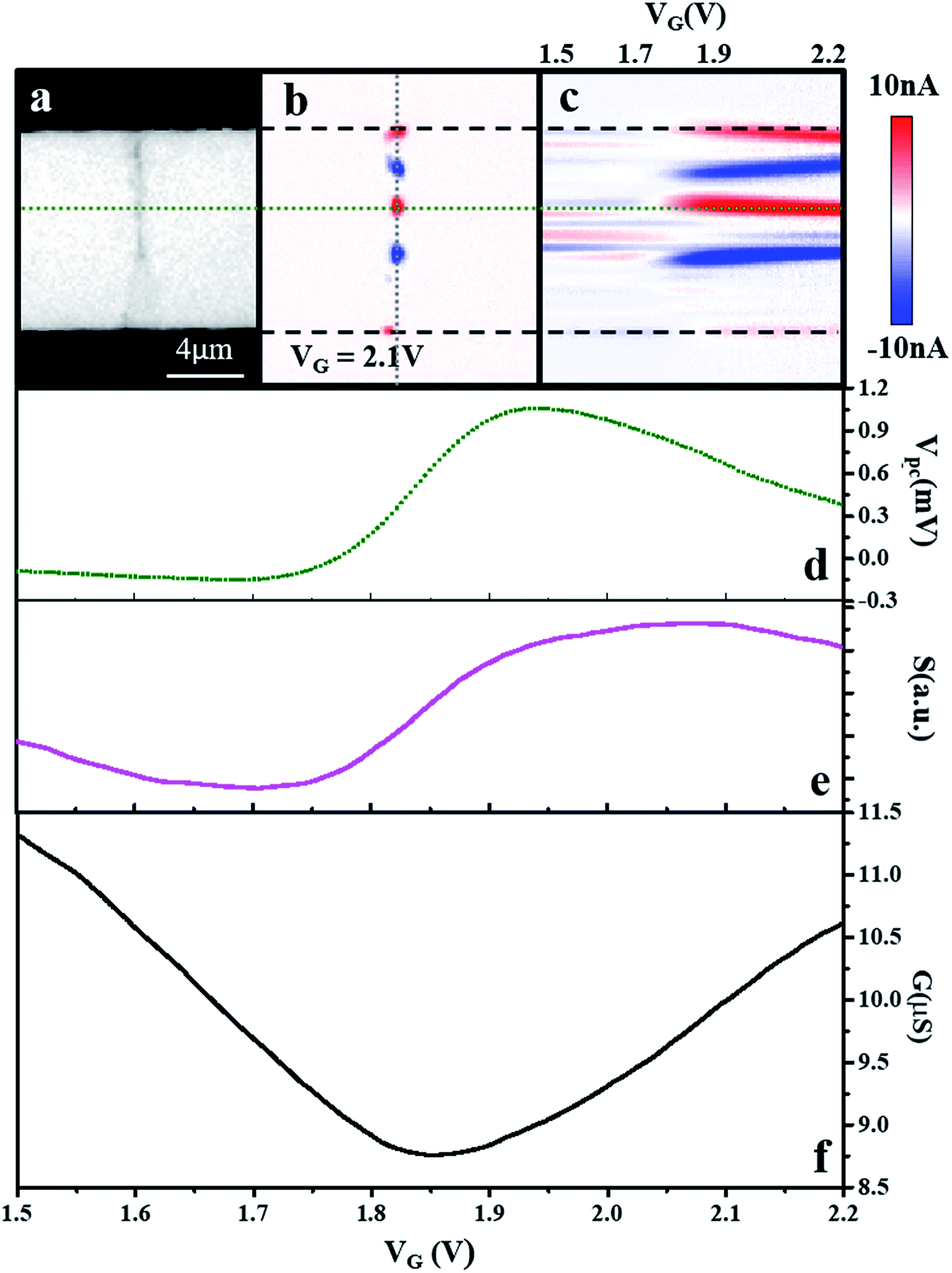 | ||
| Fig. 4 (a) Optical and (b) photocurrent images of a folded graphene ribbon with VG = 2.1 V and VDS = 0, respectively. (c) The gate-dependent scanning photocurrent image when VG varies from 1.5 V to 2.2 V. The laser scanning position is indicated by a gray dotted-line in (b). (d) Photovoltage Vpc = IpcR, where Ipc is the horizontal cut along the green dotted-lines in (c). (e) Seebeck coefficient and (f) conductance of the folded graphene ribbon transistor as a function of VG. The laser power was 0.5 mW for all photocurrent images. The trench edges are marked by the black dashed-lines. | ||
Conclusion
We report a simple strategy to alter the morphology of a suspended graphene ribbon through laser-induced local heating and in situ monitor its electrical and optoelectronic properties. Electrical transport measurements reveal that the graphene folding process results in an increase in its conductance followed by a decrease upon further folding, likely owing to the nature of the folding patterns in graphene. Scanning photocurrent microscopy measurements further show that this folding process can induce strong photocurrent signals in a deeply-folded region of graphene. Moreover, a series of folded structures can be created along the entire graphene ribbon, illustrating the capability to locally tuning the optoelectronic properties of graphene via a laser beam. Further experimental results suggest that strong photocurrent responses in folded graphene structures primarily contribute to the PTE. Our fundamental studies not only provide a way to manipulate the morphology and the electrical/optoelectronic properties of graphene, but also shed light on the underlying mechanisms of these folded graphene structures, opening up avenues to build next-generation graphene-based electronics and optoelectronics with desired properties.Conflicts of interest
The authors declare no competing financial interests.Acknowledgements
This work was supported by the National Science Foundation (ECCS-1810088), the National Institutes of Health (1R01EY027729), and Vanderbilt Discovery Grant. Devices were fabricated at the Center for Nanophase Materials Science at the Oak Ridge National Laboratory.References
- S. Chen and G. Shi, Adv. Mater., 2017, 29, 1605448 CrossRef.
- H. Tian, M. L. Chin, S. Najmaei, Q. S. Guo, F. N. Xia, H. Wang and M. Dubey, Nano Res., 2016, 9, 1543–1560 CrossRef CAS.
- G. R. Bhimanapati, Z. Lin, V. Meunier, Y. Jung, J. Cha, S. Das, D. Xiao, Y. Son, M. S. Strano, V. R. Cooper, L. Liang, S. G. Louie, E. Ringe, W. Zhou, S. S. Kim, R. R. Naik, B. G. Sumpter, H. Terrones, F. Xia, Y. Wang, J. Zhu, D. Akinwande, N. Alem, J. A. Schuller, R. E. Schaak, M. Terrones and J. A. Robinson, ACS Nano, 2015, 9, 11509–11539 CrossRef CAS PubMed.
- Z. Sun and H. Chang, ACS Nano, 2014, 8, 4133–4156 CrossRef CAS PubMed.
- F. H. Koppens, T. Mueller, P. Avouris, A. C. Ferrari, M. S. Vitiello and M. Polini, Nat. Nanotechnol., 2014, 9, 780–793 CrossRef CAS.
- S. Ogawa, M. Shimatani, S. Fukushima, S. Okuda, Y. Kanai, T. Ono and K. Matsumoto, Opt. Eng., 2019, 58, 1–6 Search PubMed.
- K. I. Bolotin, K. J. Sikes, Z. Jiang, M. Klima, G. Fudenberg, J. Hone, P. Kim and H. L. Stormer, Solid State Commun., 2008, 146, 351–355 CrossRef CAS.
- F. Schwierz, Nature, 2011, 472, 41–42 CrossRef CAS PubMed.
- W. Zhu, T. Low, V. Perebeinos, A. A. Bol, Y. Zhu, H. Yan, J. Tersoff and P. Avouris, Nano Lett., 2012, 12, 3431–3436 CrossRef CAS.
- S. K. Deng and V. Berry, Mater. Today, 2016, 19, 197–212 CrossRef CAS.
- A. Sadrzadeh, M. Hua and B. I. Yakobson, Appl. Phys. Lett., 2011, 99, 013102 CrossRef.
- P. Koskinen, Appl. Phys. Lett., 2011, 99, 013105 CrossRef.
- J. Zhang, J. Xiao, X. Meng, C. Monroe, Y. Huang and J. M. Zuo, Phys. Rev. Lett., 2010, 104, 166805 CrossRef.
- K. Kim, Z. Lee, B. D. Malone, K. T. Chan, B. Aleman, W. Regan, W. Gannett, M. F. Crommie, M. L. Cohen and A. Zettl, Phys. Rev. B: Condens. Matter Mater. Phys., 2011, 83, 245433 CrossRef.
- H. Chen, X. L. Zhang, Y. Y. Zhang, D. Wang, D. L. Bao, Y. Que, W. Xiao, S. Du, M. Ouyang, S. T. Pantelides and H. J. Gao, Science, 2019, 365, 1036–1040 CrossRef CAS PubMed.
- M. K. Blees, A. W. Barnard, P. A. Rose, S. P. Roberts, K. L. McGill, P. Y. Huang, A. R. Ruyack, J. W. Kevek, B. Kobrin, D. A. Muller and P. L. McEuen, Nature, 2015, 524, 204–207 CrossRef CAS.
- K. E. Kitko, T. Hong, R. M. Lazarenko, D. Ying, Y. Q. Xu and Q. Zhang, Nat. Commun., 2018, 9, 796 CrossRef.
- X. Li, W. Cai, J. An, S. Kim, J. Nah, D. Yang, R. Piner, A. Velamakanni, I. Jung, E. Tutuc, S. K. Banerjee, L. Colombo and R. S. Ruoff, Science, 2009, 324, 1312–1314 CrossRef CAS PubMed.
- R. Wang, T. Hong and Y. Q. Xu, ACS Appl. Mater. Interfaces, 2015, 7, 5233–5238 CrossRef CAS.
- C. J. L. De La Rosa, J. Sun, N. Lindvall, M. T. Cole, Y. Nam, M. Löffler, E. Olsson, K. B. Teo and A. J. A. P. L. Yurgens, Appl. Phys. Lett., 2013, 102, 022101 CrossRef.
- T. Hong, T. Wang and Y.-Q. Xu, Nano Lett., 2018, 18, 7883–7888 CrossRef CAS.
- T. M. G. Mohiuddin, A. Lombardo, R. R. Nair, A. Bonetti, G. Savini, R. Jalil, N. Bonini, D. M. Basko, C. Galiotis, N. Marzari, K. S. Novoselov, A. K. Geim and A. C. Ferrari, Phys. Rev. B: Condens. Matter Mater. Phys., 2009, 79, 205433 CrossRef.
- A. C. Ferrari, Solid State Commun., 2007, 143, 47–57 CrossRef CAS.
- D. Yoon, Y.-W. Son and H. Cheong, Phys. Rev. Lett., 2011, 106, 155502 CrossRef PubMed.
- Y. Zhang, K. H. Dodson, R. Fischer, R. Wang, D. Li, R. M. Sappington and Y.-Q. Xu, Nanoscale, 2016, 8, 19043–19049 RSC.
- R. Wang, M. J. Shi, B. Brewer, L. J. Yang, Y. C. Zhang, D. J. Webb, D. Y. Li and Y. Q. Xu, Nano Lett., 2018, 18, 5702–5708 CrossRef CAS.
- T. Mueller, F. Xia, M. Freitag, J. Tsang and P. Avouris, Phys. Rev. B: Condens. Matter Mater. Phys., 2009, 79, 245430 CrossRef.
- S. Lee, Y. Jo, S. Hong, D. Kim and H. W. Lee, Curr. Opt. Photonics, 2017, 1, 7–11 CrossRef CAS.
- A. W. Tsen, L. Brown, M. P. Levendorf, F. Ghahari, P. Y. Huang, R. W. Havener, C. S. Ruiz-Vargas, D. A. Muller, P. Kim and J. Park, Science, 2012, 336, 1143–1146 CrossRef CAS.
- I. Silvestre, A. W. Barnard, S. P. Roberts, P. L. McEuen and R. G. Lacerda, Appl. Phys. Lett., 2015, 106, 153105 CrossRef.
- W. Xu, Z. Qin, C. T. Chen, H. R. Kwag, Q. Ma, A. Sarkar, M. J. Buehler and D. H. Gracias, Sci. Adv., 2017, 3, e1701084 CrossRef.
- Z. Jarrahi, Y. Cao, T. Hong, Y. S. Puzyrev, B. Wang, J. Lin, A. H. Huffstutter, S. T. Pantelides and Y. Q. Xu, Nanoscale, 2013, 5, 12206–12211 RSC.
- W. Cai, A. L. Moore, Y. Zhu, X. Li, S. Chen, L. Shi and R. S. Ruoff, Nano Lett., 2010, 10, 1645–1651 CrossRef CAS.
- S. Chen, A. L. Moore, W. Cai, J. W. Suk, J. An, C. Mishra, C. Amos, C. W. Magnuson, J. Kang, L. Shi and R. S. Ruoff, ACS Nano, 2011, 5, 321–328 CrossRef CAS.
- C. Faugeras, B. Faugeras, M. Orlita, M. Potemski, R. R. Nair and A. K. Geim, ACS Nano, 2010, 4, 1889–1892 CrossRef CAS.
- T. Hong, Y. H. Cao, D. Ying and Y. Q. Xu, Appl. Phys. Lett., 2014, 104, 223102 CrossRef.
- R. R. Nair, P. Blake, A. N. Grigorenko, K. S. Novoselov, T. J. Booth, T. Stauber, N. M. Peres and A. K. Geim, Science, 2008, 320, 1308 CrossRef CAS PubMed.
- M. Cutler and N. F. Mott, Phys. Rev., 1969, 181, 1336–1340 CrossRef CAS.
- X. Xu, N. M. Gabor, J. S. Alden, A. M. van der Zande and P. L. J. N. l. McEuen, Nano Lett., 2009, 10, 562–566 CrossRef.
- Y. M. Zuev, W. Chang and P. Kim, Phys. Rev. Lett., 2009, 102, 096807 CrossRef.
- T. Wang and Y.-Q. Xu, Electronics, 2016, 5, 93 CrossRef.
- T. Hong, B. Chamlagain, S. Hu, S. M. Weiss, Z. Zhou and Y.-Q. Xu, ACS Nano, 2015, 9, 5357–5363 CrossRef CAS PubMed.
- X. Xu, N. M. Gabor, J. S. Alden, A. M. van der Zande and P. L. McEuen, Nano Lett., 2010, 10, 562–566 CrossRef CAS.
- T. S. Walmsley, K. Andrews, T. Wang, A. Haglund, U. Rijal, A. Bowman, D. Mandrus, Z. Zhou and Y. Q. Xu, Nanoscale, 2019, 11, 14410–14416 RSC.
Footnote |
| † Electronic supplementary information (ESI) available. See DOI: 10.1039/d0na00413h |
| This journal is © The Royal Society of Chemistry 2020 |