
 Open Access Article
 This Open Access Article is licensed under a Creative Commons Attribution-Non Commercial 3.0 Unported Licence
Polarization detection in deep-ultraviolet light with monoclinic gallium oxide nanobelts†
Quan
Chen
,
Yonghui
Zhang
 *,
Tao
Zheng
,
Zhun
Liu
,
Liangwei
Wu
,
Zhaoxiong
Wang
and
Jingbo
Li
*
*,
Tao
Zheng
,
Zhun
Liu
,
Liangwei
Wu
,
Zhaoxiong
Wang
and
Jingbo
Li
*
Institute of Semiconductors, South China Normal University, Guangzhou 510631, China. E-mail: yhzhang@m.scnu.edu.cn; jbli@m.scnu.edu.cn
First published on 15th May 2020
Abstract
Detection of polarization in deep-ultraviolet (DUV) wavelength is of great importance, especially in secure UV communication. In this paper, we report DUV polarization detectors based on ultra-wide bandgap β-Ga2O3 nanobelts, which belong to a monoclinic system with a strong anisotropic lattice structure. Single-crystalline β-Ga2O3 nanobelts are synthesized at high-temperature via chemical vapor deposition (CVD). Crystallographic investigation is performed to determine the crystal orientation of the nanobelts, by the combination of selected area electron diffraction (SAED), high-resolution transmission electron microscopy (HRTEM), crystal modeling and diffraction simulation. The photoresponse to unpolarized DUV light shows a high responsivity of 335 A W−1 and high sensitivity even to a low illumination power of pW. Strong anisotropy in responsivity and response speed, depending on incident light polarization, is observed. The underlying mechanism is attributed to the combination of internal dichroism and 1D morphology, as indicated by the DFT calculation and FDTD simulation. This work shows a way of DUV polarization detection using CVD grown Ga2O3 nanobelts, which could broaden the investigation of the Ga2O3 material and DUV photodetection.
Introduction
The detection of the polarization state in DUV wavelength is of tremendous importance, particularly, in free space ultraviolet (UV) communication.1 As almost all of the DUV light (200–280 nm) is absorbed by ozone molecules in the atmosphere, the DUV communication channels near the earth surface are essentially solar blind, i.e., no background noise and high signal to noise ratio (SNR). In the non-line-of-sight (NLOS) communication, the DUV signal could easily transmit around obstacles and terrain features. Moreover, the DUV signal becomes extinct after propagating for a certain distance rather than remaining in background, which makes it a secure communication technology in tactical applications. According to Rayleigh scattering theory, the main scattering mechanism of DUV light in signal transmission, the polarization state of the DUV light varies with the scattering angle. Therefore, the detection of the DUV polarization state is vital for efficient and accurate DUV communication. In addition, by using the polarization modulation, the data transmission rate of DUV communication would be significantly improved.1–4Some of the reports on polarization detection with critical parameters are listed in Table 1. These reports can be classified into two categories according to their detection mechanisms. The first one is presented as “dichroism”, which means that the detection mechanism is derived from the intrinsic anisotropic optical properties that are related to anisotropic crystal lattices. Actually, six among the seven crystal systems are expected to be anisotropic, except for the cubic system. Polarization detection based on monoclinic, triclinic, hexagonal, orthorhombic and tetragonal materials has been reported. The detection of the polarization state of light using anisotropic semiconductors has been studied for a long time. Since 2015, black phosphorus has been employed in polarization state detectors due to its dichroism along zigzag and armchair directions.5,6 Transition metal sulfides,7–10 group III sulfides,11 group IV sulfides,12,13 group III–IV compounds,14,15 group II–VI (ref. 16) compounds, wide-bandgap oxides16–18 and perovskites19 are also found to have an anisotropic response to polarized light. It is worth noting that high quality single crystallinity is the prerequisite in this type of polarization detector. The other type of mechanism is presented as “morphology”, which means that the detection mechanism is related to the attenuated electric field that results from the large dielectric contrast between 1D materials (nanowires, nanorods and nanobelts) and the surrounding environment.20–24 Finer 1D materials are preferred to increase the anisotropy. Generally, the diameter of 1D materials should be much smaller than the excitation wavelength, while the crystallinity is not a key factor. Of course, the two mechanisms may work together and lead to higher anisotropy.19 The references in Table 1 are arranged in the order of optical bandgaps from large to small. Narrow bandgap semiconductors may have broader response spectra from visible to middle infrared (VIS-MIR), while wide bandgap semiconductors have the advantage of wavelength selectivity as they are insensitive to photons with energy less than the bandgap. The use of wide bandgap semiconductors enables compact devices without bulky band filters.17,30 Although some of these studies report anisotropic properties in wide-bandgap semiconductors, such as GeS2 (ref. 12) (Eg = 3.71 eV), ZnO16,23 (Eg = 3.4 eV), GaN (Eg = 3.4 eV),26,31 SnO2 (ref. 25) (Eg = 3.6 eV) and MoO3 (ref. 32) (Eg = 2.7 eV), they do not reach the range of solar-blind wavelength.
| Materials | Crystal system | Anisotropic plane | Optical bandgap/eV | Detection wavelength | Material morphology | Anisotropic mechanism | Anisotropy ratio | References |
|---|---|---|---|---|---|---|---|---|
| β-Ga2O3 | Monoclinic | (−101) | 4.8 | UVC | 3D nanobelt | Dichroism | 0.96 | This work |
| β-Ga2O3 | Monoclinic | (100) | 4.53–4.76 | UVC | 3D bulk | Dichroism | 0.53(*) | 17 |
| β-GaxInyO3 | Monoclinic | (010) | 4.4–4.7 | UVC | 3D bulk | Dichroism | — | 18 |
| GeS2 | Monoclinic | (001) | 3.71 | UVA | 2D flake | Dichroism | 0.36(#) | 12 |
| SnO2 | Tetragonal | (010) | 3.6 | UVA | 3D Microwire | Dichroism | 0.39(#) | 25 |
| MZO/ZnO MQW | Hexagonal | (11−20) | 3.17–3.57 | UVA | 3D MQW | Dichroism | 0.71(#) | 16 |
| ZnO | Hexagonal | — | 3.37 | UVA | 3D nanowire | Morphology | 0.19(*) | 23 |
| GaN | Hexagonal | (11−20) | 3.4 | UVA | 3D thin film | Dichroism | 0.76(#) | 26 |
| GaN | Hexagonal | — | 3.4 | UVA–UVC | 3D nanowire | Morphology | 0.16 | 24 |
| GeSe2 | Monoclinic | (001) | 2.74 | VIS | 2D flake | Dichroism | 0.55(#) | 13 |
| GeSe2 | Monoclinic | (001) | 2.96 | VIS | 2D flake | Dichroism | 0.38(#) | 27 |
| CsPbI3 | Orthorhombic | (100) | 2.79 | VIS | 3D nanowire | Dich. & Morp. | 0.46(#) | 19 |
| CdSe | Cubic & hexagonal | — | 1.79 | VIS | 3D nanowire | Morphology | 0.13(#) | 28 |
| ZrS3 | Monoclinic | (001) | 1.79 | VIS | 2D nanoribbon | Dichroism | 0.27(#) | 9 |
| ReS2/ReSe2 | Triclinic | (001) | 1.6/1.3 | VIS | 2D heterojunction | Dichroism | 0.47(*) | 8 |
| CH3NH3PbI3 | Tetragonal | (001) | 1.58 | VIS | 3D nanowire | Morphology | 0.13(#) | 29 |
| ReS2 | Triclinic | (001) | 1.5 | VIS | 2D flake | Dichroism | 0.47(*) | 7 |
| Inp | Cubic | — | 1.35 | Visible | 3D nanowire | Morphology | 0.96 | 20 |
| TiS3 | Monoclinic | (001) | 1.13 | VIS-NIR | 2D nanoribbon | Dichroism | 0.6(#) | 10 |
| GeAs2 | Orthorhombic | (001) | 1 | VIS | 2D flake | Dichroism | 0.33(*) | 15 |
| TlSe | Tetragonal | (110) | 0.73 | VIS | 2D flake | Dichroism | 0.45(#) | 11 |
| BP | Orthorhombic | (001) | 0.3 | VIS-NIR | 2D flake | Dichroism | 0.82(*) | 5 |
| BP | Orthorhombic | (001) | 0.3 | VIS-MIR | 2D flake | Dichroism | 0.63(*) | 6 |
β-Gallium oxide (β-Ga2O3), an ultra-wide bandgap (Eg = 4.8 eV) semiconductor, has gained increasing attention in the past decade. Due to its short response edge blow 280 nm, Ga2O3 is regarded as a strong candidate in solar-blind deep-ultraviolet photodetection.33 In particular, β-Ga2O3 belongs to the monoclinic crystal structure, which has strong anisotropic properties.34–38 The theoretical study suggests that the conduction band minimum (CBM) is undivided with the irreducible representation of Γ1+, while the valence band maximum (VBM) splits into 18 bands: 6Γ1+, 3Γ2+, 3Γ1−, and 6Γ2−. According to the transition selection rule, only the transitions from the Γ1− band of the VBM to the Γ1+ band of the CBM are allowed for the electric vector E parallel to the b axis, while only the transitions from the Γ2− band of the VBM to the Γ1+ band of the CBM are allowed for E in the a–c plane, where a, b and c are the primitive vectors.37,39,40 Based on the interband transition principle, anisotropic optical absorption,39,41 reflection35 and transmission,17,37,39 as well as polarization detection42 have been reported with single crystal platelets. Compared to bulk and thin film materials, nanostructured materials are favorable for responsivity and photocurrent gain due to the increased photo-generated carriers resulting from the larger surface-to-volume ratio.43
In this paper, we report DUV polarized light photodetectors fabricated with single crystalline β-Ga2O3 nanobelts. The crystallographic investigation was conducted to determine the crystal orientation of Ga2O3 nanobelts. The Ga2O3 nanobelts were found to grow along the [202] direction, with a smaller optical bandgap and higher absorption coefficient than the perpendicular direction, as revealed by DFT calculations. The Ga2O3 nanobelt photodetector showed excellent performance to unpolarized DUV light with a responsivity of 335 A W−1 and high sensitivity even to a low incident power of pW. The anisotropic photoresponse to linearly polarized DUV light was studied, with a higher photocurrent and faster response speed along [202] than the [020] direction, which could be ascribed to the combination of intrinsic dichroism and external morphology with the former accounting for the main proportion.
Results and discussion
To take full advantage of the anisotropic crystal lattice of the monoclinic system, single-crystalline materials must be employed to ensure a long-range-order atomic arrangement. High quality single-crystalline Ga2O3 nanobelts were synthesized at high temperature with a chemical vapor deposition (CVD) system, the apparatus of which is depicted in Fig. 1(a). Details of material preparation can be found in the Experimental section. As can be seen from the transmission electron microscopy (TEM) image in Fig. 1(b), the width of the nanobelt is 280 nm, a bit larger than the wavelength of the excitation light (254 nm) in this work. The nanobelts are 50 nm-thick as determined via AFM (ESI S1†). The high-resolution TEM (HRTEM) image taken from the edge of the nanobelt [spot c in Fig. 1(b)] is shown in Fig. 1(c). The interplanar spacing along the nanobelt direction is 0.235 nm, while the perpendicular direction is 0.152 nm, corresponding to the (202) and (020) crystal planes, respectively. The selected area electron diffraction (SAED) pattern taken from the main body of the nanobelt [spot d in Fig. 1(b)] is shown in Fig. 1(d), with determined crystal plane indexes above each of the diffraction spots. The determination of each of the diffraction spots has been verified with the interplanar spacing of each plane and the angle formula between different planes. The diffraction spots in the reciprocal space constitute a deformed hexagonal pattern, rotated 90° from that in real space constructed by Ga atoms in Fig. 1(c). HRTEM and fast Fourier transform (FFT), conducted at several other spots, show a similar character, indicating that most area of the nanobelt is a single crystal (ESI S2†). According to the Weiss zone law, we find out the direction of the crystal zone axis to be [−101]. Then, the crystal structure model with the same orientation and view direction was constructed and is shown in Fig. 1(e). After hiding oxygen atoms, the same deformed hexagonal pattern can be seen in Fig. 1(f), with each vertex constructed by a chain of gallium atoms. The interplanar spacing along the [020] and [202] direction is 0.152 nm and 0.235 nm, respectively, in good agreement with the experimental results in Fig. 1(c). The simulated electron diffraction pattern with the same projection direction is shown in Fig. 1(g), with the stereographic projection direction in the up-left corner. The crystal plane indexes from the simulation are in good agreement with those derived in Fig. 1(d). The X-ray diffraction, taken from many randomly stacked nanobelts, confirms the β-phase of the Ga2O3 nanobelts and the existence of determined crystal planes. The consistency of simulation and experimental results suggests the correctness of the determination of the crystal orientation.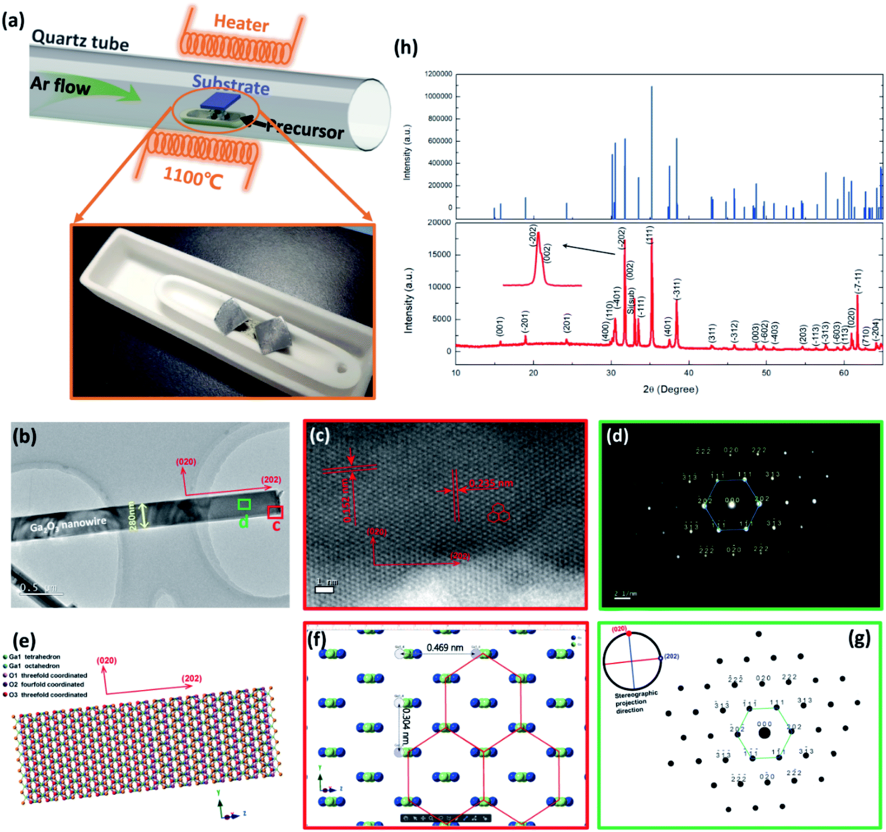 | ||
| Fig. 1 Crystallographic study of Ga2O3 nanobelts. (a) Schematic of the CVD system used in Ga2O3 nanobelt growth. (b) TEM image of a Ga2O3 nanobelt. (c) HR-TEM image of the Ga2O3 nanobelt where atoms are in a deformed hexagonal arrangement. (d) SAED image of the Ga2O3 nanobelt with determined crystal plane indexes above each of the diffraction spots. (e) Crystal structure model in the same view direction as the nanobelt. (f) Structure of Ga atoms that are in the same deformed hexagon arrangement as that in (c). (g) Simulated electron diffraction pattern using the same direction as that in (d). (h) Comparison between X-ray diffraction results of β-Ga2O3 nanobelts and that in the standard PDF card. | ||
The DUV polarization detector devices were fabricated on flexible substrates in the MSM structure with Ti/Au electrodes [Fig. 2(a)]. To characterize the response of the devices to DUV light, current–voltage (I–V) characteristics were studied under the illumination of 254 nm DUV light. Fig. 2(b) shows the illumination–power-dependent I–V characteristics while the device was bent to a radius of 8 mm, corresponding to a tensile strain of 0.77%, with no degeneration of device performance compared to that in the flat state. Further increasing the strain level would not deteriorate the Ga2O3 nanobelt, however, a crack might occur in Ti/Au electrodes. The photocurrent characteristics at a strain of 0.64%, 0.49% and 0% can be find in ESI S3.† The mechanical robustness of the flexible device also demonstrates its potential in volatile tactical applications. The DUV photodetector was found to have a supersensitive response to DUV light, even in the pico watt range. While increasing the illumination power (P), the photocurrent (Iph) increased according to a simple power law of Iph = P0.69 [Fig. 2(c)], the non-unity of the exponent indicating the recombination process of photogenerated electrons and holes. Taking the illumination area as 8.4 × 10⁻⁸ cm2 [the product of the nanobelt width (280 nm) and electrode spacing (L = 30 μm)], the responsivity (R) of the device varies with irradiated photo power, with a maximum responsivity of 335 A W−1 at 2.64 pW. Typically, responsivity higher than the theoretical value (0.205 A W−1 for 254 nm according to R0= qλ/hc, where R0 is the intrinsic responsivity) indicates an internal gain (G) in the photodetector. Assuming the external quantum efficiency (η) to be 100%, internal gain in this device is calculated to be 1640 according to G = R × (hc)/(λqn), where h is Plank's constant, c is the velocity of light and q is the elementary charge. Nanoscale photodetectors usually show a high responsivity and gain due to their high surface-to-volume ratio.44,45 For this Ga2O3 nanobelt device, carrier traps may exist on the surface of the nanobelt owing to the surface energy fluctuation resulting from the dangling bond and surface adsorption. In the above context, we suppose that a hole is trapped in a surface state while the corresponding electron is striding under the drive of an electrical field. If the trap has not released the hole before the electron reaches its collecting electrode, to maintain electrostatic balance, the electron has to circulate in the loop before the hole was released, resulting in high gain and responsivity. The trapping states essentially prolonged the lifetime (τ) of the carriers by preventing electrons and holes from recombination.46 In addition, the carrier transit time (τt) is shortened with a high voltage bias of 50 V. As a consequence, the ratio of prolonged carrier lifetime and shortened transit time yields a large gain via G = τ/τ. The normalized gain (GN), a parameter which reflects intrinsic photoconduction efficiencies, is calculated to be 2.95 × 10⁻⁴ cm2 V−1 through GN = Gη(L2/V).47 For space communication, a large UVC/UVA rejection ratio is favorable to suppress the noise from the background. The photodetector exhibits a much higher response to 254 nm than to 365 nm light, showing a high UVC/UVA rejection ratio of 3500 [Fig. 2(d)]. To characterize the response speed of the DUV detector, the time resolved photoresponse [Fig. 2(e)] tests were conducted at 0.5 Hz frequency using an electric shutter. The uniform photoresponse character demonstrates the reliability of the Ga2O3 nanobelt photodetector. Enlarging one of the repeated cycles, the rising and falling time were found to be 33 ms [Fig. 2(f)] and 40 ms [Fig. 2(g)], respectively. The high performance of the flexible photodetector confirmed the high quality of Ga2O3 nanobelts and Ga2O3/Ti/Au interfaces, which are prerequisites of the following DUV polarization detection.
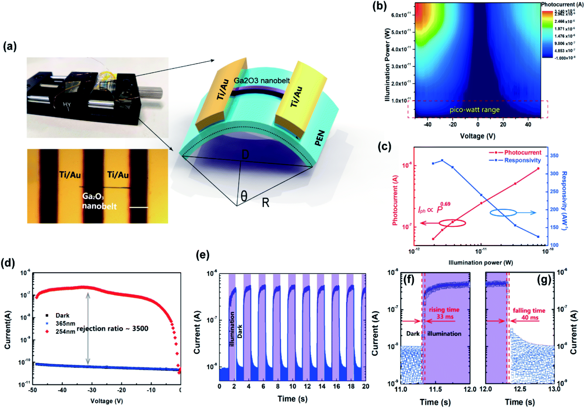 | ||
| Fig. 2 Device characteristics with unpolarized DUV illumination. (a) Schematics of the flexible Ga2O3 nanobelt photodetector. (b) Illumination–power-dependent I–V characteristics. (c) Diagram of photocurrent and responsivity versus illumination power. (d) Photocurrent under UV254 nm irradiation compared with that under UV365 nm irradiation. (e) Time-resolved photoresponse characteristics with V = 50 V. (f) Rising and (g) falling edge of one photoresponse cycle. | ||
The anisotropic photoresponse characteristics were measured with linearly polarized DUV light provided by a wire grid polarizer placed in front of the device, the configuration of which is shown in the inset of Fig. 3(a). The photocurrent of 0°, 45°, 90° and 135° polarized light resembles that of 180°, 225°, 270° and 315°, respectively [Fig. 3(a)], exhibiting a central symmetry character. By changing the polarization angle via rotating the polarizer and light source, the photocurrent varied accordingly, as can be seen in Fig. 3(b). Strong anisotropic photoresponse properties can be observed, with the maximum photocurrent in 0° and 180° directions and the minimum in 90° and 270° directions. The maximum photoconductivity anisotropy ratio, σ = (I// − I⊥)/(I// + I⊥), where I//(I⊥) is the photocurrent with parallel (perpendicular) polarization, is 0.96 at V = 17 V. The 2D colour map of photocurrent versus voltage and the polarization angle is shown in Fig. 3(c), in which two-fold symmetry can be found in one cycle, consistent with the central symmetric crystal structure in Fig. 1(c). To estimate the effect of the polarization angle on the response speed, time resolved photoresponse tests were performed at V = 10 V at various angles [Fig. 3(d)] from 0° to 360° in 10° step. Overlaying 0° to 90° curves, the modulation on photocurrent intensity can be clearly observed as in Fig. 3(e). After normalizing the photocurrent curves, the dependency of response speed on the polarization angle can be seen in Fig. 3(f). The rising and falling time increased from 0.7 s to 2.7 s and from 0.06 s to 0.15 s, respectively, when increasing the polarization angle from 0° to 90°. The overall longer response time compared to those in Fig. 2(f) and (g) can be attributed to the much smaller voltage bias (1 V) used here. Anisotropic rising and falling photoresponse speed are summarized in Fig. 3(g). Obviously, the photoresponse speed is higher to 0° polarized DUV light, while lower to 90° polarized DUV light. Since the active material is a low-symmetric monoclinic nanobelt, both the dichroism and morphology mechanisms could contribute to the anisotropic character. As the width of the nanobelt [Fig. 1(b)] is larger than the excitation wavelength, the contribution to the anisotropic photoresponse from the morphology factor should be small.20,28 To estimate the anisotropy that arose from the 1D morphology, finite-difference time-domain (FDTD) simulation was performed. The simulation results yield a low anisotropic ratio of 0.13 under 254 nm irradiation for 280 nm wide nanobelts (ESI S4†), suggesting that the morphology mechanism is not the main factor. Then, density functional theory (DFT) calculation was employed to evaluate the contribution from dichroism. It was found out that the optical absorption coefficient α is 6.5 times larger when the electric vector E is parallel to the [202] direction than that when the E is parallel to the [020] direction at 4.88 eV (254 nm). Considering the negative correlation between the optical band gap and absorption coefficient,48 the result is quite straightforward, since the optical bandgap is larger when E is parallel to the b axis.35,37 With fewer photons absorbed when E is parallel to the [020] direction, fewer photocarriers could be generated, and thus a smaller photocurrent is expected when the polarization angle is perpendicular to the nanobelt. With more photons absorbed by Ga2O3, more electrons would transit from the valence band to the conduction band. The photogeneration and recombination reach equilibrium at a higher speed, and therefore, a faster response speed is achieved when E is parallel to the [202] direction.
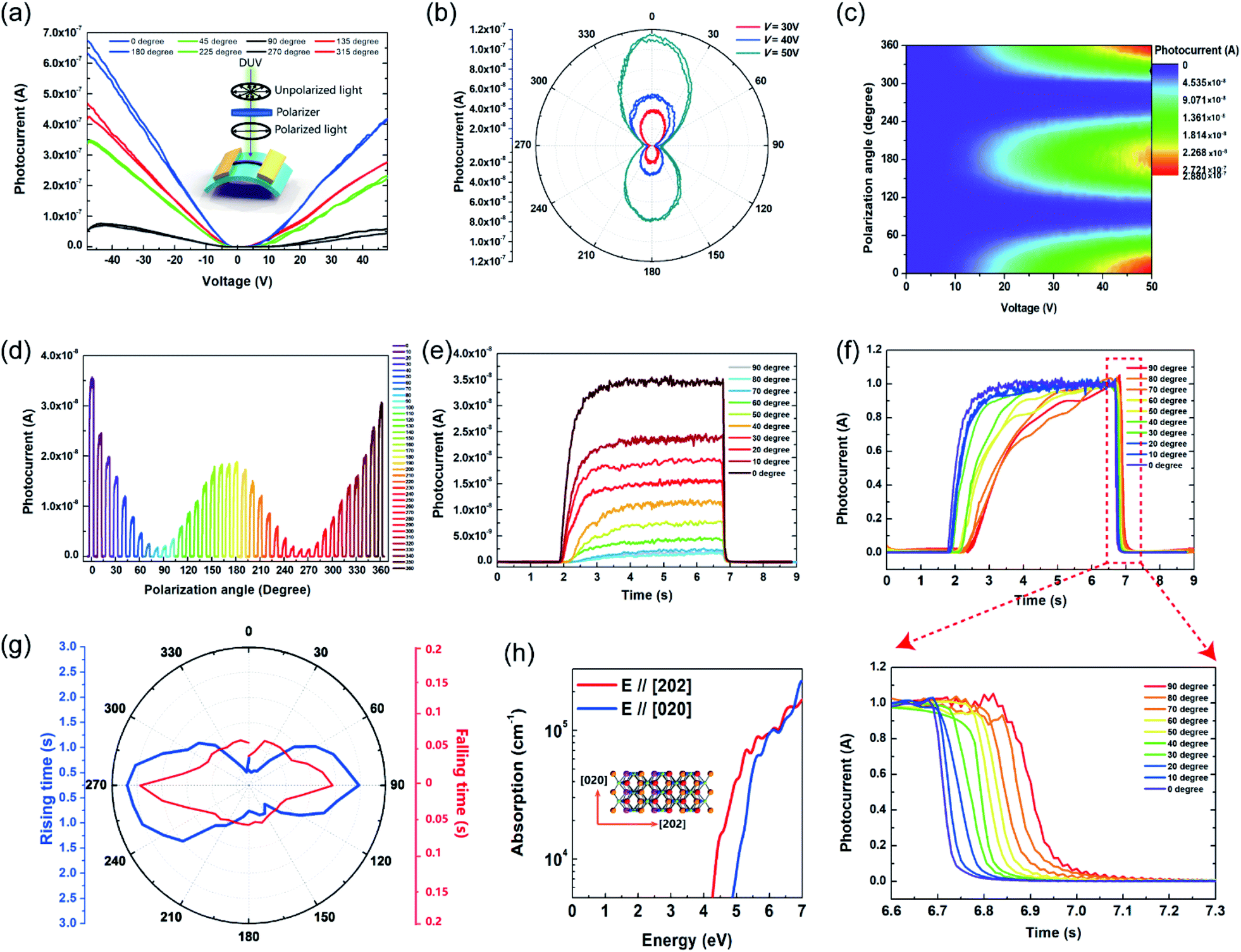 | ||
| Fig. 3 Detection of DUV polarized light. (a) I–V characteristics under the illumination of DUV with different polarization angles. (b) Diagram of photocurrent versus polarization angle at different voltage bias. (c) 2D colour map of photocurrent with independent variables of both voltage and polarization angles. (d) Time-resolved photoresponse under DUV with varied polarization angles from 0–360°. (e) Photoresponse of DUV with polarization angles from 0–90°, where the photocurrent was modulated. (f) Normalized photoresponse of DUV at different polarization angles, where the rising and falling speed changed. (g) Summary of rising and falling time versus the polarization angle. (h) Absorption coefficient along [020] and [202] directions from the DFT calculation. | ||
Conclusions
In summary, DUV polarized light photodetection is realized based on low-symmetrical monoclinic single-crystalline Ga2O3 nanobelts. The nanobelts are grown along the [202] direction as revealed by the crystallographic study, with the b axis, which possesses a larger optical bandgap and smaller absorption coefficient, along the perpendicular direction. The DUV photodetector exhibits an excellent response to unpolarized DUV light, with high sensitivity even to pico watt and a high responsivity of 335 A W−1. Better still, the Ga2O3 nanobelt photodetector shows an obvious anisotropic response to linearly polarized DUV light. Both the photocurrent intensity and photoresponse speed are higher when the polarization direction is parallel to the nanobelt, which is ascribed to the combination of intrinsic dichroism and 1D morphology mechanisms, with the former accounting for the main proportion. The realization of DUV polarization state detection using monoclinic Ga2O3 nanobelts might broaden the application of the thriving Ga2O3 semiconductor, and further promote the development of DUV photodetection.Experimental section
Material preparation and characterization
Ga2O3 nanobelts were synthesized by CVD at 1100 °C in an argon atmosphere, using Ga2O3 and carbon powder as the precursor and reductant, respectively. To start with, Si wafer was ultrasonically cleaned in acetone and absolute alcohol, followed by decoration with gold nanoparticles. After one hour synthesis of Ga2O3 nanobelts in the CVD system (length range from 40–100 μm), the sample was naturally cooled down to room temperature. The Ga2O3 nanobelts were then stripped into absolute alcohol by the ultrasonic dispersion method, after which they were transferred onto polyethylene naphthalate (PEN) substrates for the use of device fabrication. X-ray diffraction was conducted with a Bruker D8 Advance diffractometer. SAED and HRTEM characteristics were performed using JEM-2100 HR transmission electron microscopy.Device fabrication and tests
Ga2O3 nanobelt photodetectors were fabricated using an interdigitated patterned metal mask (feature size of 30 μm). Ti/Au electrodes were deposited using an electron beam evaporation system. The 254 nm DUV light was provided by a Luyor Lpx-254 ultraviolet lamp, the optical power of which was measured using a Linshang LS125 UV light meter. Linearly polarized light was produced with a Thorlabs WP25M-UB wire grid polarizer. The photocurrent was recorded with a Keithley 2614B sourcemeter.Crystal modeling and diffraction simulation
The crystal modeling and electron diffraction simulation in Fig. 1 were performed with Crystal maker X 10.2.2 and Singlecrystal 3.1.1. Lattice parameters used in this work is from the crystallography open database (COD-2004987).DFT calculations
First-principles calculations are carried out by using the plane-wave pseudopotential approach as implemented in the software of Vienna Ab Initio Simulation Package (VASP). The electron–core interactions are treated by the projected augmented wave pseudopotentials and the exchange and correlation functional was used in the Perdew–Burke–Ernzerhof (PBE) parametrizations of GGA for structural relaxation calculations. The optimized lattices for the bulk phase β-Ga2O3 are 12.46, 3.08, and 5.88 Å for the a, b and c axis, with an axis angle of 90°, 103.7°, and 90°, respectively. These calculated parameters are slightly expanded with respect to the experiments. The lattice axis directions of the crystal structure are further reoriented to match with the nanobelt axis for the anisotropic optical absorption calculations. We further used the PBE0 functional for the absorption spectrum corrections. The electronic minimization was performed with a tolerance of 10−6 eV, and ionic relaxation was performed with a force tolerance of 0.005 eV Å−1 on each ion. The Ga 3s, 3p, and 3d electrons are treated as valence states. The kinetic energy cutoff was set as 520 eV, and the k-point mesh was used with a grid spacing of less than 2π × 0.15 Å−1.Conflicts of interest
The authors declare no conflict of interest.Acknowledgements
This work is financially supported by the “The Pearl River Talent Recruitment Program” and National Natural Science Foundation of China (Grant No. 11674310). The authors are grateful for the technical support from the School of Materials and Energy, Guangdong University of Technology.Notes and references
- A. Vavoulas, H. G. Sandalidis, N. D. Chatzidiamantis, Z. Xu and G. K. Karagiannidis, IEEE Commun. Surv. Tutor., 2019, 21, 2111–2133 Search PubMed.
- H. Yin, H. Jia, H. Zhang, X. Wang, S. Chang and J. Yang, J. Opt. Soc. Am. A, 2011, 28, 2082 CrossRef PubMed.
- H. Zhang, H. Yin, H. Jia, S. Chang and J. Yang, Appl. Opt., 2012, 51, 8366 CrossRef PubMed.
- H. Yin, H. Jia, H. Zhang, X. Wang, S. Chang and J. Yang, SPIE Security + Defence, ed. E. M. Carapezza and H. J. White, Edinburgh, United Kingdom, 2012, p. 85400I Search PubMed.
- T. Hong, B. Chamlagain, T. Wang, H.-J. Chuang, Z. Zhou and Y.-Q. Xu, Nanoscale, 2015, 7, 18537–18541 RSC.
- H. Yuan, X. Liu, F. Afshinmanesh, W. Li, G. Xu, J. Sun, B. Lian, A. G. Curto, G. Ye, Y. Hikita, Z. Shen, S.-C. Zhang, X. Chen, M. Brongersma, H. Y. Hwang and Y. Cui, Nat. Nanotechnol., 2015, 10, 707–713 CrossRef CAS PubMed.
- F. Liu, S. Zheng, X. He, A. Chaturvedi, J. He, W. L. Chow, T. R. Mion, X. Wang, J. Zhou, Q. Fu, H. J. Fan, B. K. Tay, L. Song, R.-H. He, C. Kloc, P. M. Ajayan and Z. Liu, Adv. Funct. Mater., 2016, 26, 1169–1177 CrossRef CAS.
- D. Liu, J. Hong, X. Wang, X. Li, Q. Feng, C. Tan, T. Zhai, F. Ding, H. Peng and H. Xu, Adv. Funct. Mater., 2018, 28, 1804696 CrossRef.
- X. Wang, K. Wu, M. Blei, Y. Wang, L. Pan, K. Zhao, C. Shan, M. Lei, Y. Cui, B. Chen, D. Wright, W. Hu, S. Tongay and Z. Wei, Adv. Electron. Mater., 2019, 5, 1900419 CrossRef.
- S. Liu, W. Xiao, M. Zhong, L. Pan, X. Wang, H.-X. Deng, J. Liu, J. Li and Z. Wei, Nanotechnology, 2018, 29, 184002 CrossRef PubMed.
- S. Yang, C. Hu, M. Wu, W. Shen, S. Tongay, K. Wu, B. Wei, Z. Sun, C. Jiang, L. Huang and Z. Wang, ACS Nano, 2018, 12, 8798–8807 CrossRef CAS PubMed.
- Y. Yang, S.-C. Liu, X. Wang, Z. Li, Y. Zhang, G. Zhang, D.-J. Xue and J.-S. Hu, Adv. Funct. Mater., 2019, 29, 1900411 CrossRef.
- Y. Yang, S.-C. Liu, W. Yang, Z. Li, Y. Wang, X. Wang, S. Zhang, Y. Zhang, M. Long, G. Zhang, D.-J. Xue, J.-S. Hu and L.-J. Wan, J. Am. Chem. Soc., 2018, 140, 4150–4156 CrossRef CAS PubMed.
- L. Li, W. Wang, P. Gong, X. Zhu, B. Deng, X. Shi, G. Gao, H. Li and T. Zhai, Adv. Mater., 2018, 30, 1706771 CrossRef PubMed.
- L. Li, P. Gong, D. Sheng, S. Wang, W. Wang, X. Zhu, X. Shi, F. Wang, W. Han, S. Yang, K. Liu, H. Li and T. Zhai, Adv. Mater., 2018, 30, 1804541 CrossRef PubMed.
- G. Tabares, A. Hierro, B. Vinter and J.-M. Chauveau, Appl. Phys. Lett., 2011, 99, 071108 CrossRef.
- X. Chen, W. Mu, Y. Xu, B. Fu, Z. Jia, F.-F. Ren, S. Gu, R. Zhang, Y. Zheng, X. Tao and J. Ye, ACS Appl. Mater. Interfaces, 2019, 11, 7131–7137 CrossRef CAS PubMed.
- V. I. Vasyltsiv, Ya. I. Rym and Ya. M. Zakharko, Phys. Status Solidi B, 1996, 195, 653–658 CrossRef CAS.
- Y. Zhou, J. Luo, Y. Zhao, C. Ge, C. Wang, L. Gao, C. Zhang, M. Hu, G. Niu and J. Tang, Adv. Opt. Mater., 2018, 6, 1800679 CrossRef.
- J. Wang, M. S. Gudiksen, X. Duan, Y. Cui and C. M. Lieber, Science, 2001, 293, 1455–1457 CrossRef CAS PubMed.
- Y. Gao, L. Zhao, Q. Shang, Y. Zhong, Z. Liu, J. Chen, Z. Zhang, J. Shi, W. Du, Y. Zhang, S. Chen, P. Gao, X. Liu, X. Wang and Q. Zhang, Adv. Mater., 2018, 30, 1801805 CrossRef PubMed.
- S. Niu, G. Joe, H. Zhao, Y. Zhou, T. Orvis, H. Huyan, J. Salman, K. Mahalingam, B. Urwin, J. Wu, Y. Liu, T. E. Tiwald, S. B. Cronin, B. M. Howe, M. Mecklenburg, R. Haiges, D. J. Singh, H. Wang, M. A. Kats and J. Ravichandran, Nature Photon, 2018, 12, 392–396 CrossRef CAS.
- Z. Fan, P. Chang, J. G. Lu, E. C. Walter, R. M. Penner, C. Lin and H. P. Lee, Appl. Phys. Lett., 2004, 85, 6128–6130 CrossRef CAS.
- S. Han, W. Jin, D. Zhang, T. Tang, C. Li, X. Liu, Z. Liu, B. Lei and C. Zhou, Chem. Phys. Lett., 2004, 389, 176–180 CrossRef CAS.
- L. Li, W. Gao, H. Chen, K. Zhao, P. Wen, Y. Yang, X. Wang, Z. Wei, N. Huo and J. Li, Adv. Electron. Mater., 2020, 1901441, DOI:10.1002/aelm.201901441.
- C. Rivera, J. L. Pau, E. Muñoz, P. Misra, O. Brandt, H. T. Grahn and K. H. Ploog, Appl. Phys. Lett., 2006, 88, 213507 CrossRef.
- Y. Yan, W. Xiong, S. Li, K. Zhao, X. Wang, J. Su, X. Song, X. Li, S. Zhang, H. Yang, X. Liu, L. Jiang, T. Zhai, C. Xia, J. Li and Z. Wei, Adv. Opt. Mater., 2019, 7, 1900622 CrossRef CAS.
- A. Singh, X. Li, V. Protasenko, G. Galantai, M. Kuno, H. Xing and D. Jena, Nano Lett., 2007, 7, 2999–3006 CrossRef CAS PubMed.
- L. Gao, K. Zeng, J. Guo, C. Ge, J. Du, Y. Zhao, C. Chen, H. Deng, Y. He, H. Song, G. Niu and J. Tang, Nano Lett., 2016, 16, 7446–7454 CrossRef CAS PubMed.
- M. Razeghi and A. Rogalski, J. Appl. Phys., 1996, 79, 7433–7473 CrossRef CAS.
- S. Ghosh, C. Rivera, J. L. Pau, E. Muñoz, O. Brandt and H. T. Grahn, Appl. Phys. Lett., 2007, 90, 091110 CrossRef.
- M. Zhong, K. Zhou, Z. Wei, Y. Li, T. Li, H. Dong, L. Jiang, J. Li and W. Hu, 2D Mater., 2018, 5, 035033 CrossRef.
- R. Tang, G. Li, C. Li, J. Li, Y. Zhang, K. Huang, K. Huang, J. Ye, J. Ye, C. Li, J. Kang, R. Zhang, R. Zhang and Y. Zheng, Opt. Express, 2020, 28, 5731–5740 CrossRef PubMed.
- C. Kranert, C. Sturm, R. Schmidt-Grund and M. Grundmann, Sci. Rep., 2016, 6, 1–9 CrossRef PubMed.
- T. Matsumoto, M. Aoki, A. Kinoshita and T. Aono, Jpn. J. Appl. Phys., 1974, 13, 1578 CrossRef CAS.
- T. Onuma, S. Fujioka, T. Yamaguchi, Y. Itoh, M. Higashiwaki, K. Sasaki, T. Masui and T. Honda, J. Cryst. Growth, 2014, 401, 330–333 CrossRef CAS.
- N. Ueda, H. Hosono, R. Waseda and H. Kawazoe, Appl. Phys. Lett., 1997, 71, 933–935 CrossRef CAS.
- M. Zhao, R. Tong, X. Chen, T. Ma, J. Dai, J. Lian and J. Ye, Opt. Mater., 2020, 102, 109807 CrossRef CAS.
- T. Onuma, S. Saito, K. Sasaki, T. Masui, T. Yamaguchi, T. Honda and M. Higashiwaki, Jpn. J. Appl. Phys., 2015, 54, 112601 CrossRef.
- K. Yamaguchi, Solid State Commun., 2004, 131, 739–744 CrossRef CAS.
- Y. Wang, P. T. Dickens, J. B. Varley, X. Ni, E. Lotubai, S. Sprawls, F. Liu, V. Lordi, S. Krishnamoorthy, S. Blair, K. G. Lynn, M. Scarpulla and B. Sensale-Rodriguez, Sci. Rep., 2018, 8, 1–7 CrossRef PubMed.
- X. Chen, Y. Xu, D. Zhou, S. Yang, F. Ren, H. Lu, K. Tang, S. Gu, R. Zhang, Y. Zheng and J. Ye, ACS Appl. Mater. Interfaces, 2017, 9, 36997–37005 CrossRef CAS PubMed.
- J. Kim, S. Oh, S. Kim and J. Kim, in Gallium Oxide, ed. S. Pearton, F. Ren and M. Mastro, Elsevier, 2019, pp. 331–368 Search PubMed.
- H. Chen, K. Liu, L. Hu, A. A. Al-Ghamdi and X. Fang, Mater. Today, 2015, 18, 493–502 CrossRef CAS.
- L. Sang, M. Liao and M. Sumiya, Sensors, 2013, 13, 10482–10518 CrossRef CAS PubMed.
- Y. Li, T. Tokizono, M. Liao, M. Zhong, Y. Koide, I. Yamada and J.-J. Delaunay, Adv. Funct. Mater., 2010, 20, 3972–3978 CrossRef CAS.
- R. S. Chen, H. Y. Tsai, Y. S. Huang, Y. T. Chen, L. C. Chen and K. H. Chen, Appl. Phys. Lett., 2012, 101, 113109 CrossRef.
- R. A. Smith, Semiconductors, Cambridge University Press, Cambridge, 2nd edn, 1978 Search PubMed.
Footnote |
| † Electronic supplementary information (ESI) available. See DOI: 10.1039/d0na00364f |
| This journal is © The Royal Society of Chemistry 2020 |