
 Open Access Article
 This Open Access Article is licensed under a Creative Commons Attribution-Non Commercial 3.0 Unported Licence
Broadband transparency with all-dielectric metasurfaces engraved on silicon waveguide facets: effect of inverted and extruded features based on Babinet's principle
Alina
Karabchevsky
 *,
Eran
Falek
,
Yakov
Greenberg
,
Michael
Elman
,
Yaakov
Keren
and
Ioseph
Gurwich
*,
Eran
Falek
,
Yakov
Greenberg
,
Michael
Elman
,
Yaakov
Keren
and
Ioseph
Gurwich
School of Electrical and Computer Engineering, Ben-Gurion University, Beer-Sheva 8410501, Israel. E-mail: alinak@bgu.ac.il
First published on 3rd June 2020
Abstract
Building blocks of photonic integrated circuitry (PIC), optical waveguides, have long been considered transparent. However, the inevitable Fresnel reflection from waveguide facets limits their transparency. This limitation becomes more severe in high-index waveguides in which the transparency may drop to 65%. We overcome this inherent optical property of high-index waveguides by engineering an appropriate facet landscape made of sub-wavelength artificial features unit cells. For this, we develop a semi-analytical formalism for predicting the metasurface parameters made of high-index dielectric materials, to be engraved on the facets of optical waveguides, based on Babinet's principle: either extruded from the waveguide facet or etched into it. Our semi-analytical model predicts the shape of anti-reflective metasurface unit cells to achieve transmission as high as 98.5% in near-infrared from 1 μm to 2 μm. This new class of metasurfaces may be used for the improvement of PIC devices for communication and sensing, where device transparency is crucial for high signal-to-noise ratios.
1 Introduction
Passive optical waveguides are widely used for transferring signals between two physical locations within a chip.1–8 A single semiconductor chip with a common area of several mm2 can include up to several hundred optical waveguides. These chips are commonly used in cameras, telescopes, multiplexers, devices that include on-chip laser, filters, light sources, amplifiers, and other optical devices.3–6 However, the fact that an optical waveguide is embedded in a semiconductor chip limits the material choices for constructing the waveguide to those that are commonly used in the semiconductor industry. Due to their unique guiding properties, high-index core waveguides made of semiconductor materials such as silicon, silicon-nitride, gallium arsenide, etc., are very commonly used in fields ranging from communications, interconnectors and biosensors9 to switching, multiplexing, division and mode conversion. As a result of the high refractive index of the semiconductor core materials,10 such on-chip waveguides suffer from low transmission efficiency. One of the main reasons for this low efficiency is the inevitable Fresnel reflection from the high refractive index facet. Commonly used silicon and gallium arsenide, having indexes of around 4, cause the optical signal to lose about 30% of its energy at the inward transition between the air medium and the core material of the waveguide.9 Being transferred through in- and out-waveguide facets, the optical signal loses about 51% of its energy just due to these air-semiconductor media transitions. Clearly, such losses are very significant and result from the inherent properties of the materials. Conventional waveguides, such as those used in passive fiber-optics2,11 with silica glass-core, only lose about 4% of their energy at the transition from the air to the fiber-optic glass-core, and vice versa, therefore this efficiency problem is much less significant in passive glass-based optical fibers.Despite the vast research published on optical transparency, very little is known about how to make optical waveguide transparent via sculpturing their facets with metasurfaces. For example, inside the absorption region one can use electromagnetic-induced-transparency (EIT) equivalent structures, made either of metals or all-dielectric materials e.g., silicon.12–15 These structures are utilizing the outside-generated energy to introduce a transparent region inside the absorption region. In a Si or GaAs waveguide, however, the excitation in a transparent region, and the losses they experience, are due to the reflection but not absorption.
One typical prior art solution to the efficiency problem mentioned above suggests the application of coatings such as aluminum, aluminum oxide, barium fluoride, calcium fluoride, cerium(IV) oxide, and others to the input and output facets of an optical waveguide. This typically reduces reflections in a specific spectrum range.16–21 However, the above coatings are not applicable to avoid reflections on the tiny surfaces of polished waveguide facets. Even where the deposition of a coating is possible, this solution still suffers from another problem: in harsh conditions, the coating tends to crack and even gets off the core. This is particularly noticeable in environments of high temperature, high-pressure or environmental stress changes, such as in airplanes, satellites, high-power devices and space stations. Matching oils are widely used to minimize Fresnel reflection. However, they are mainly suitable for a laboratory environments.
Changing the landscape of the waveguide facet at the nanoscale was proposed to avoid reflection;22–24 however, a broadband anti-reflection property for waveguides was never achieved. It is, therefore, the object of the present work to report on improving the efficiency of on-chip waveguides having high-index core, by obtaining broadband transparency. While developing the methodology to improve the transmission efficiency of waveguides, we set a goal: to study silicon particle-based metasurfaces25–31 in order to maximize the mean value of transmission at a given spectral range. The on-facet metasurfaces possess two fundamental properties: (1) a gradient index profile between two optically coupled media, and (2) a light trapping effect. To demonstrate the transparency effect in waveguides we developed the semi-analytical method, which allows for predicting the shape of the unit cell and its parameters.
The following sections provide the theory as well as numerical proof-of-concept simulations exploring the properties of dielectric metasurfaces engraved in – or extruded from – the waveguide facets, to study the waveguide transparency effect.
2 Unit-cell shape: analytical description
When exploring the maximization of transmission through a waveguide, one must first eliminate the absorbency of the waveguide medium, i.e., choose the proper spectral range. However, when dealing with metasurfaces on facets, determining the non-absorption band is not a trivial task. This is due to the light trapping effect, which significantly increases the contribution to the overall absorption.32It is well known that for a single wavelength, one can obtain almost zero reflection.33 However, any widening of the spectral range affects the reflection at this specific wavelength. In the present analytical description, we consider the minimization of the mean value reflection at a given spectral range, together with minimizing the deviation value.
The choice of the unit cell for the metasurface is also not trivial since neither the shape nor the geometry are prescribed by general theoretical arguments. Therefore, let us consider a periodic arbitrarily shaped metasurface on a waveguide facet (Fig. 1a).
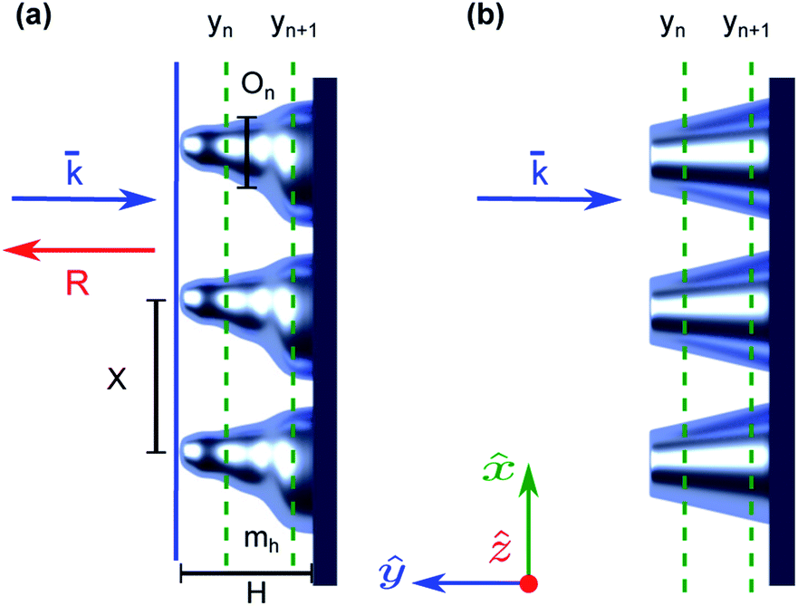 | ||
Fig. 1 Schematics of (a) an arbitrarily shaped metasurface engraved on waveguide facet with of refractive index mh is represented as a layered system consisting of yn layers. Incident illumination is indicated by the vector ![[k with combining macron]](https://www.rsc.org/images/entities/i_char_006b_0304.gif) . Light reflected from the facet is indicated by R. σn is the area of unit cells in nth layer made of index mh. H indicates the height of a unit-cell, X is the period of the structure, On is the filling parameter. (b) The optimal structure according to the formulation is a linear σ(y), which in 2D configuration imply a cone structure. . Light reflected from the facet is indicated by R. σn is the area of unit cells in nth layer made of index mh. H indicates the height of a unit-cell, X is the period of the structure, On is the filling parameter. (b) The optimal structure according to the formulation is a linear σ(y), which in 2D configuration imply a cone structure. | ||
All parameters of the considered structure, except its total width, are small in comparison to the incident wavelength λ in a vacuum.
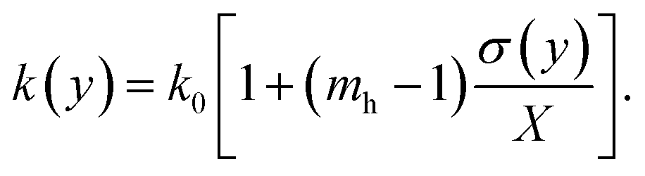
Next, we divide the facet into infinitesimally thin layers yn. Since the structure is sub-wavelength, the formalism of effective medium theory can be used. In addition, under the geometrical optics approach, we approximate the description to one in which the higher-order scattering is ignored. Assuming the period of the structure is X < λ, the height is designated as H (which is unknown at this point), and the refractive index of the medium as mh. If we denote σn as the part of the period filled by the medium in the nth layer, then the effective refractive index in this layer can be estimated as:
 | (1) |
Considering the normal incidence illumination, the reflection rn from the boundary between nth and (n + 1)th layers is
 | (2) |
At the upper surface of the facet (blue solid line in Fig. 1), the contribution of rn is
 | (3) |
The wave number k(y) can be written as
 | (4) |
Generally, the reflection of a layered structure is represented by the bulk relation, where the analysis of such representation is a relatively cumbersome task. Here, we restrict ourselves by assuming that: |rn| ≪ 1, and also that the transmitted wave approximately preserves its amplitude; in other words, |tn| ≈ 1. In the framework of this approximation, the total reflection can be written as 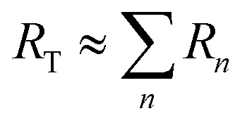 , and represented by the integral as
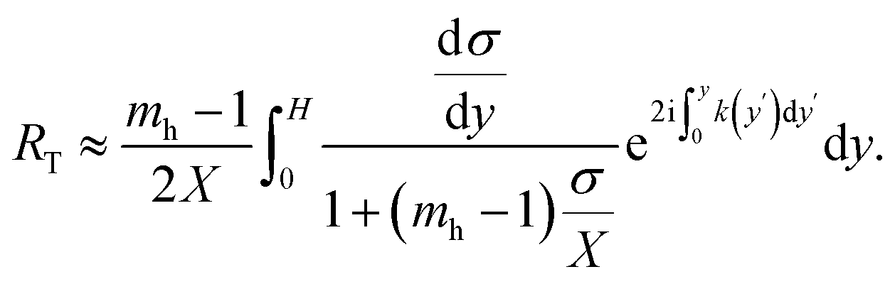 | (5) |
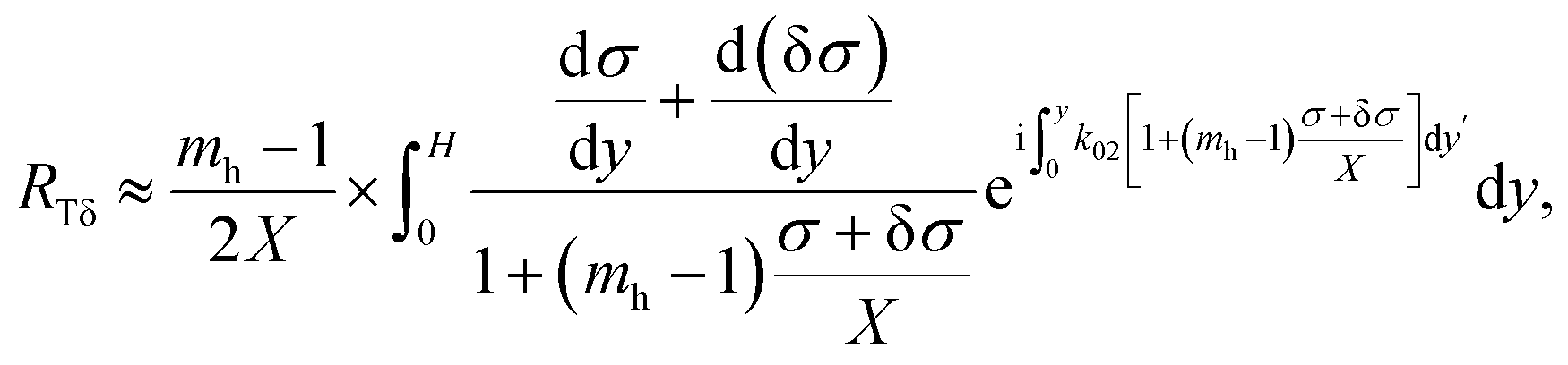
The absolute value of RT has to be minimized. We solve this minimization problem for a monochromatic wave. Dealing with a fixed H, the problem can be defined as a variational one. The shape of the unit-cell, which is represented by σ(y), will now be determined. Suppose δσ is a small variation of σ(y); then the total reflection for this new unit-cell is
 | (6) |
 | (7) |
 | (8) |
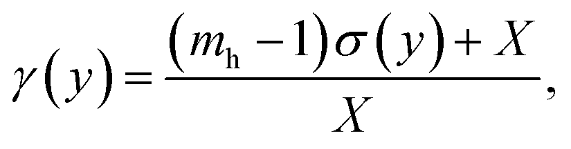
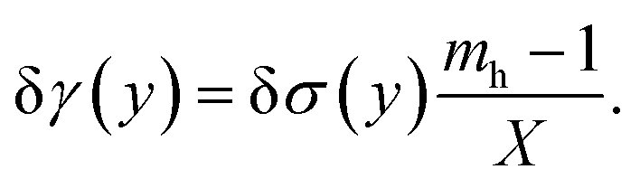
For simplicity, we denote the function σ(y) by σ and γ(y) by γ. In terms of γ(y), eqn (6) takes the form of
 | (9) |
For obtaining γ(y) in a closed form, we assume that the function  is an order smaller than ‖δγ‖ (o(‖δγ‖)), where ‖δγ‖ is a certain norm of δγ in the interval y ∈ [0, H]. While this may be not correct for an arbitrary δγ, and an arbitrary y, at least for small H, the integral contribution of wrong y points will be small.
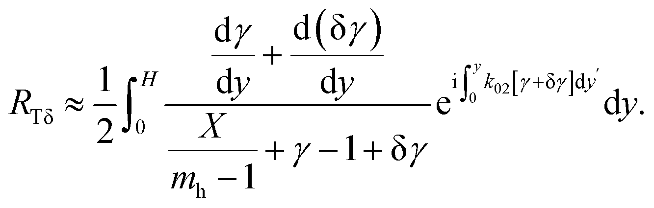
In the framework of the above-mentioned assumption 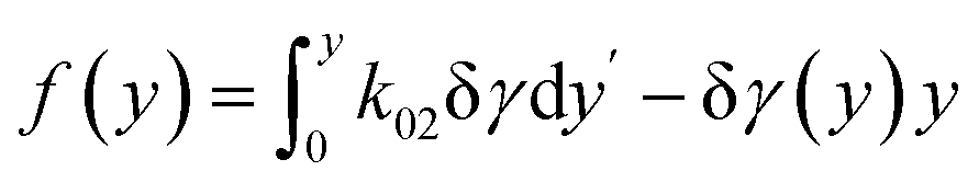 , we obtain the variation of RTδ as
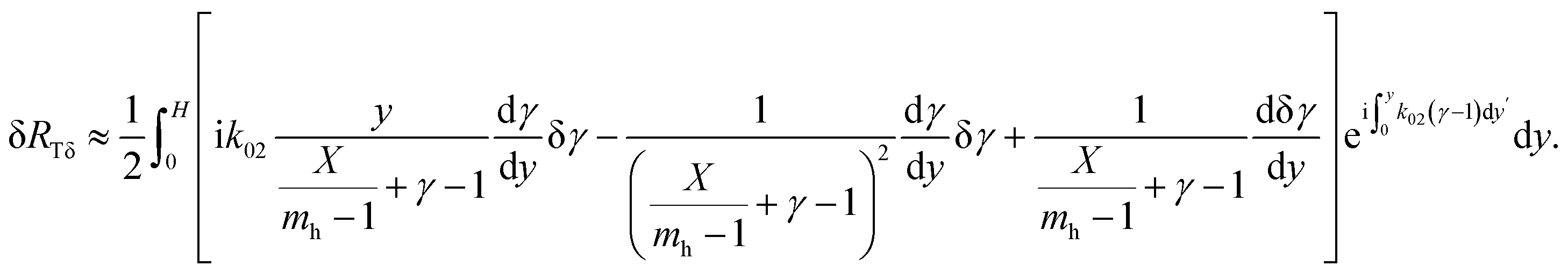 | (10) |
After integrating the term  by parts, the real part vanishes, and we obtain a simplified form of δRTδ as
 | (11) |
According to calculus of variations, we set δRTδ = 0, and thus, the eqn (11) leads to
 | (12) |
In eqn (12), the point y = 0 is singular and should be treated with care, since also γ − 1 = 0, and thus, (γ − 1)/y are undefined at y = 0. Therefore, one should choose a trajectory for integration in the complex plane. By doing so, the solution γ = 1 + Cy is obtained, and the integration constant C can be taken as 1 without lost of generality.
Then, for σ(y) the following is obtained:
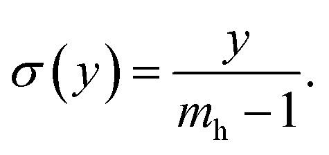 | (13) |
Eqn (13) describes a linear dependence of the y-level fill-factor on y. It shows that each unit-cell has a constant slope. This prescribes a conical or pyramidal shape of the unit-cells as shown in Fig. 1b.
Analytically obtained optimal shape of a unit-cell providing anti-reflection can be found in the state of the art experimental studies.22,35–38 We stress, however, that although explored experimentally, the correct parameters of these structures have not yet been obtained as optimal ones to suppress reflection in a broad spectral range.
A linear function for the filling fraction σ(y) implies that the effective refractive index is also linear in y according to eqn (1). In Fig. 2 we show the transmittance as a result of a plane-wave incident on a half plane with refractive index ns = 3.5. At the interface of the incidence we added a gradient index matching layer with thickness H. The matching layer was divided into slices with a thickness of 10 nm, where every slice had a refractive index according to the linear function
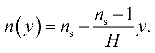 | (14) |
 | ||
| Fig. 2 The transmittance as a function of wavelength as a result of a plane wave incident on a half-plane with a refractive index ns = 3.5. A linear gradient index matching layer is applied to the interface of the half-plane. The gradient index layer thickness is H. The incident wave is propagating and being reflected in vacuum. | ||
The structure was simulated based on transfer-matrix method39 to obtain the transmittance of this structure. In Fig. 2 one can notice that the transmittance is significantly higher than 69%, which is the direct transmittance from a half-plane with n = 3.5. One can also notice that the transmittance does not exhibit any resonant behavior. In other words, the anti-reflection property holds for wide bandwidth.
By taking into account higher-order effects such as multiple scattering, the shape can be modified, and the new form can be calculated by solving numerically the wave-equation for waveguide systems. However, if we consider that σ(H) = X, it is immediately obtained from eqn (13) that H = X(mh − 1). Therefore, the above assumption with respect to a small value of H is justified for mh close enough for 1. This justifies also the main assumption about the small value of |rn|, and thus the possibility of ignoring the multiple scattering.
Based on the gradient index (GRIN) optics, it can also be stated that the lowest reflection can be achieved by structuring the entire area of the waveguide facet with the metasurface. This means that the optimal filling factor On of the facet prescribes unit-cells being densely distributed on the facet. Otherwise, a step change of the refractive index would occur at the layer where y = H. The arguments above also show a weak effect of the randomization of the unit-cells location on the facet: such a process generally contradicts the requirement of dense spatially distributed unit-cells within the metasurface.
The trapping of photons also contributes to the transmission. Therefore, the value of H predicted above turns out to be overestimated. It is also expected that multiple scattering would contribute more in the bottom layers than in the upper ones. It is plausible to estimate the likelihood of every trapped photon (and thus, contribution to transmission) by the additional factor of ρ2τ/s, where ρ is the reflectance of each unit-cell, τ is the transmittance through the metasurface, and s is the distance between interacting unit-cells. This difference between the upper base du and the bottom base db in the multi-scattering process may be corrected by fitting the shape of the truncated cone by a paraboloid.
3 Proof-of-concept numerical results
While considering structures on the waveguide facet of a high refractive index, the multiple scattering effects should also be considered. Therefore, the shape of the unit-cells should be confirmed by calculations taking into account multiple scattering contributions. Here, therefore, we report also on a numerical model and proof-of-concept calculations.Based on our theoretical evaluations described in the previous sections, we found that a periodic lattice made of densely distributed cones minimizes the reflection effect. To prove this, we built a full-wave numerical simulation using Lumerical and CST Finite-Difference-Time-Domain (FDTD) solvers and calculated the optical characteristics of an arbitrary waveguide. In our numerical investigation, we consider the rib waveguide with the structure depicted in Fig. 3a. This contains the silicon guiding layer (Si, n = 3.4784 (ref. 40)) on silicon-dioxide substrate (SiO2, n = 1.444 (ref. 41)) with rib width of W = 10 μm, height T = 2.4 μm and rib height t = 0.5 μm. We note that the unit cell is extruded from the same material as the waveguide. The calculated fundamental TE mode profile is shown in Fig. 3e.
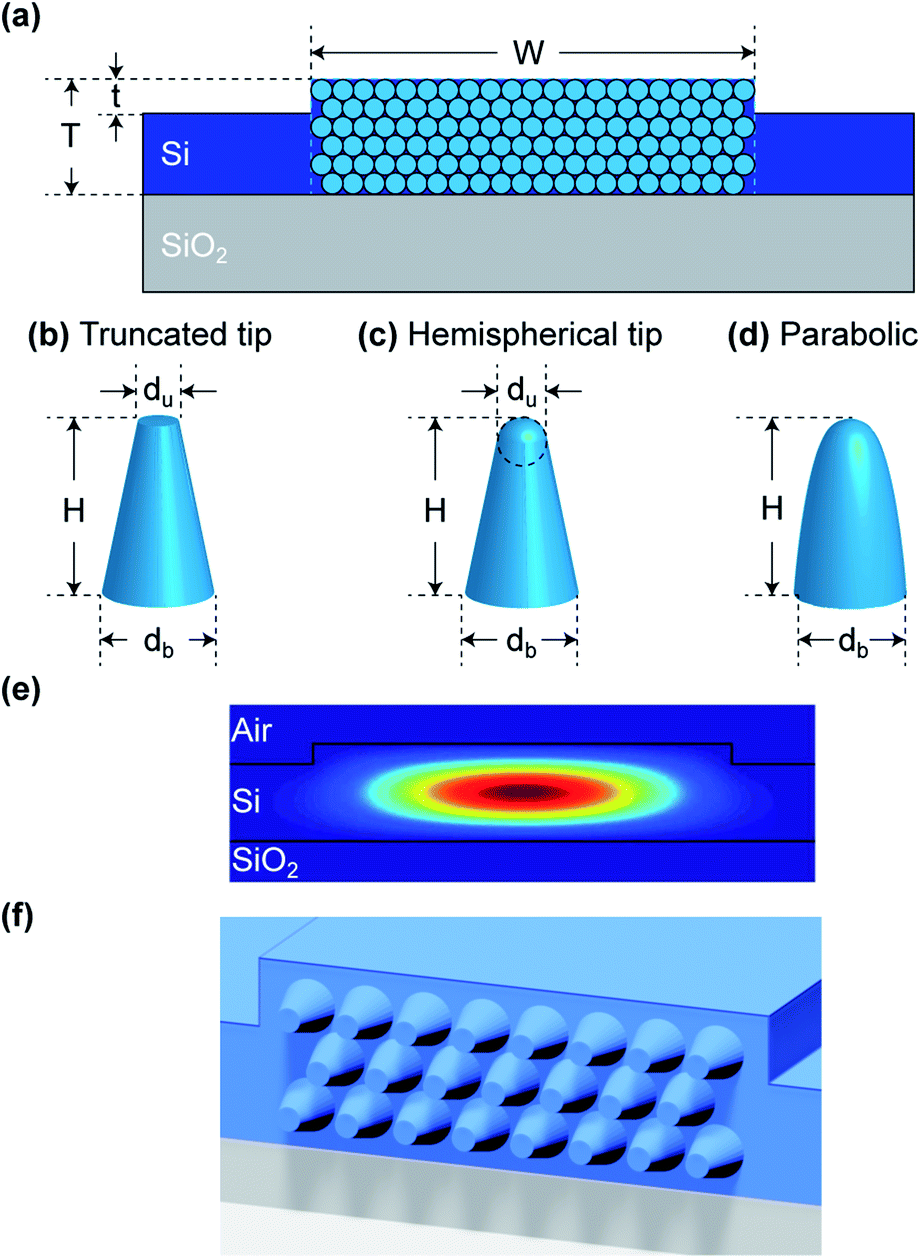 | ||
| Fig. 3 (a) Schematic cross-section of the silicon rib waveguide facet; rib width W of 10 μm, height T of 2.4 μm and silicon nanostrip thickness t of 0.5 μm with engraved silicon metasurface made of unit-cells of conical shape with: (b) truncated tip, (c) hemispherical tip and (d) parabolic tip. (e) Calculated fundamental TE mode profile for the smooth waveguide facet. (f) 3D illustration of the extruded conical structures from the facet. | ||
It is important to stress, that even though the silicon waveguides can be produced with smaller cross-sections, which is commonly used to support a single mode propagation, the proposed AR structure is not mode dependent and works well also for the multi-mode waveguides. In addition, as the cross-section area increases, the array of cones becomes larger, which improves the collective effect of the structure as a metasurface, and reduces the effects caused by the edges. Smaller cross-section would require smaller unit-cells, which is more challenging to fabricate. For these reasons a larger cross-section was chosen in our simulation. In the numerical model, we launch the Gaussian beam into the waveguide with a radius of 1.5 μm where the waist (focal point) is 1.5 μm from the source. The beam is directed in parallel to the waveguide axis z and polarized linearly to the y direction. The facet is placed at a distance of 1.5 μm where the beam focuses. The center of the beam is aligned with the center of the waveguide guiding layer such that maximal power is incident upon the facet. This anticipates realistic experimental conditions, where fiber is butt-coupled to the waveguide. Since the beam spot profile is larger than the dimensions of the waveguide facet, it leads to the beam-facet mismatch losses. We calculate the transmission by integrating the power flow in the z direction at a distance of 2 μm from the facet (the plane of the cone bases). The integration is done over the area of the facet, i.e., x ∈ [−5, 5] μm, and y ∈ [0, 2.4] μm. The integrated power was normalized to 1 watt, which is the total power of the Gaussian beam source.
To estimate the sensitivity to different structural parameters of the conical shape unit cells, we modeled a hexagonal lattice of truncated cones (Fig. 3b) placed on the facet and adjacent to each other such as in Fig. 3a. The hexagonal grid was chosen over a rectangular one since it is more efficient due to the larger fill-factor and was chosen for our numerical test as seen in Fig. 3a. The transmission spectrum as a function of wavelength for several cone heights H is shown in Fig. 4a. The cone base db and upper du diameters are kept constant at db = 550 nm and du = 200 nm, respectively.
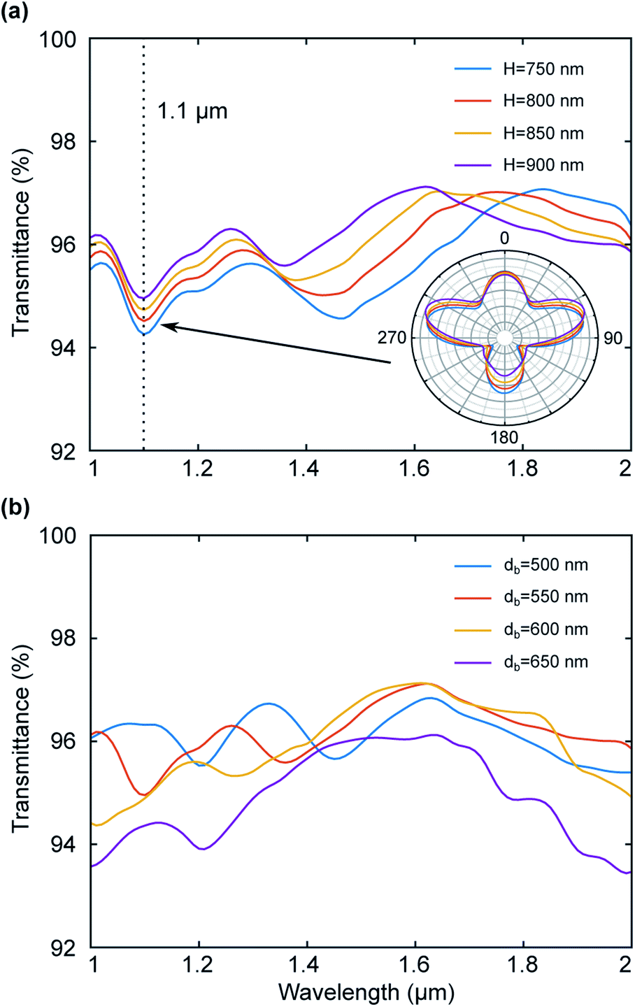 | ||
| Fig. 4 (a) Transmission spectrum as a function of wavelength for hexagonal array of truncated cones on a rib waveguide facet for different cone heights. The cone base and upper diameters are db = 550 nm and du = 200 nm, respectively. (b) Transmission spectrum for the metasurface with hexagonal grid made of truncated cones on a rib waveguide facet for different cone base diameters. The cone height and upper diameters are H = 900 nm and du = 200 nm, respectively. | ||
One can see from Fig. 4a that as the cone height increases, the overall average transmission increases as well. Although theoretically higher cones may produce better performance, practically, the larger aspect ratio of the cones (height vs. base diameter) is limited due to fabrication constraints. One can also notice the dip at 1100 nm, which is a result of a resonance due to the periodic structure. At that particular wavelength, the period of the structure is exactly λ/2. To understand the influence of height on the transmission, while neglecting the collective effect, we calculated the scattering angular diagrams of the unit cells of truncated conical shape (Fig. 3b) for the wavelength of 1100 nm from Fig. 4a. Inset of Fig. 4a shows that when the particle height increases, backward scattering is suppressed while allowing the angular dependence of the forward scattering effect.
Next, we study the sensitivity of the transmission to the base diameter db of the unit-cell. Fig. 4b shows the transmission spectrum as a function of wavelength for an hexagonal array of truncated cones with varying base diameters while the height and upper diameters are fixed at H = 900 nm and du = 200 nm, respectively.
Base diameter of db = 550 nm (red line in Fig. 4b) exhibits the highest transmission over the chosen spectral range with ![[T with combining macron]](https://www.rsc.org/images/entities/i_char_0054_0304.gif) = 96.2% with H = 900 nm. The base diameter is closely related to the periodicity of the structure, which in turn affects the spectral behavior of the device. The change of the base diameter affects the filling factor and therefore affects the transmission.
= 96.2% with H = 900 nm. The base diameter is closely related to the periodicity of the structure, which in turn affects the spectral behavior of the device. The change of the base diameter affects the filling factor and therefore affects the transmission.
The transmission of = 96.2% was obtained for the cone height of H = 900 nm and the base diameter of db = 550 nm.
Decomposing a unit cell of the periodic grid made of truncated cones into its Fourier components can explain why it yields worse performance characteristics compared to the cones with the hemispherical tip or of paraboloidal shape. The decrease in performance occurs since more energy is carried in higher diffraction orders. The orders destructively interfere with each other and reduce the overall transmission. Thus, the smoothing of the sharp edges of the cones results in a more uniform transmission in a required spectral band.
The transmission spectrum as a function of wavelength for different cone shapes is shown in Fig. 5a with the cones distributed in a hexagonal grid. This allows comparison of the performance characteristics for different tip shapes, such as truncated tip and a parabolic tip, as shown in Fig. 3b–d. In addition, we maximized the filling factor of the facet by decreasing the base unit-cell diameter db, against the previous estimations. As a result, the diameter leading to the highest transmission occurred when db = 450 nm. The height and upper diameter for the truncated tip cones are kept constant at H = 900 nm and du = 200 nm, respectively.
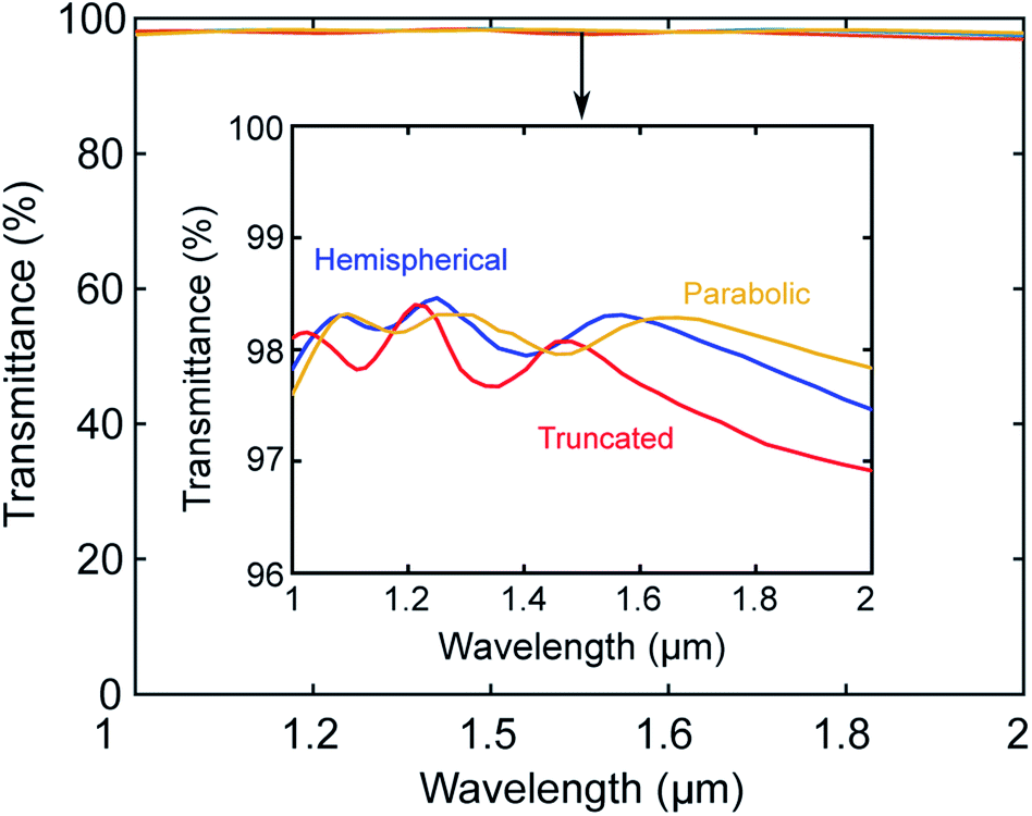 | ||
| Fig. 5 Transmission through the waveguide with engraved metasurface on its facet having the conical shape of the unit cells with the height of H = 900 nm, the lower diameter of db = 450 nm and of different tip shapes: hemispherical tip, truncated tip and parabolic tip. Inset shows zoomed transmission exhibiting spectral variations for waveguide output signal when the unit cell is of different tip shapes. | ||
Fig. 5a shows the averaged transmission as high as 98.13% in the wavelengths range from 1 μm to 2 μm using cones with parabolic tips (Fig. 3d) in the hexagonal grid. Fig. 5b shows the reflection spectrum from the input waveguide facet. The facet has an hexagonal grid of conical unit cells with db = 450 nm and H = 900 nm.
While changing the shape of the unit-cells, we analyze the results based on the diffraction grating model. Minimizing the overall reflection involves minimizing the reflection of some orders of this grating. This can also be formulated as a π phase shift at the diffraction angle β = π/2. Since the beam is incident upon the facet from the air medium, the requirement dictates the relation H = λ0/2 for a chosen wavelength of λ0. Considering the spectral range λ ∈ [λmin, λmax], it would be natural to take λ0 = (λmin + λmax)/2. However, for a wide spectral range, this can lead to an appearance of the reflection maximum at the shortest wavelength.
3.1 Influence of the tip shape
To explore the effect of the tip shape on the far-field scattering, we calculated the angular diagrams of scattered electric and magnetic fields shown in Fig. 6 for the conical particles of the truncated tip and hemispherical tip shapes. Fig. 6a and b show 3D scattering patterns of scattered electric field amplitude for the particles with hemispherical and truncated tip shapes respectively. Higher transmission for the metasurface containing particles with hemispherical tip (compared to truncated) can be seen in Fig. 5 for the wavelength of 1100 nm, which can be explained by the 2D analysis of the far-field scattering patterns shown in Fig. 6c and d, for the single particles. Particles with hemispherical tip experience a stronger forward scattering effect compared to particles with truncated tip. For both hemispherical and truncated tips, the backward scattering of the electric field is suppressed.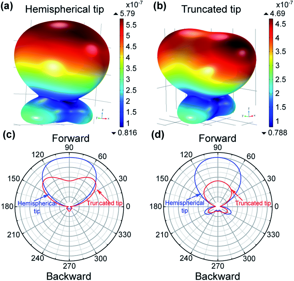 | ||
| Fig. 6 Far-field 3D scattering patterns of silicon particle of truncated-cone shape with H = 900 nm at λ wavelength of 1100 nm and illumination direction is from the tip, for: (a) spherical tip and (b) truncated tip; normalized to the maximum 2D directivities for (c) the plane of the incident electric field polarization; (d) the plane of the incident magnetic field polarization. | ||
We note that the structures we predicted can be fabricated using conventional focus ion beam (FIB) machine. Beginning with a smooth facet, the FIB machine can etch the facet based on a pre-programmed computer-aided design (CAD), and remove material, to produce the facet as in Fig. 3. For example, a FIB machine, Thermo Fisher Scientific, dual-beam G3, can be used to create the truncated cones.
3.2 Exploring inverted-tips structures based on Babinet's principle
In the previous sections, an AR structure was explored with extruded unit cells out of the waveguide facet. Although such a structure is very interesting from a fundamental point of view, it is challenging in terms of fabrication. In order to fabricate such a structure, one has to grow layers of silicon through cumbersome processes following several stages, including masking of the facets. However, according to Babinet's principle, the diffraction pattern from an opaque body is identical to that from a hole of the same size and shape, except for the overall forward beam intensity.42 Therefore, according to this principle, the fabrication process can be facilitated by means of inverted features drilled into the waveguide facet. This may be realized by employing techniques such as FIB. In this section, we discuss the structure shown in Fig. 7.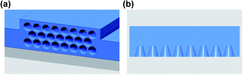 | ||
| Fig. 7 Inverted-tips structure as an AR metasurface. (a) An illustration of an hexagonal array of conical holes etched in waveguide facet. (b) The cross-section of a row of conical holes on waveguide facet. | ||
First, we explore the influence of truncated cone shapes on AR properties of the waveguide facet. To this end, we integrate the power flow in the z direction behind the structure, at a distance of 2.5 μm from the facet. The choice of this distance is dictated by the overall simulation sizes. The unit-cells distribution is chosen to be hexagonal, the same as was done in the extruded structures case. In addition, we integrate the power inside the waveguide (the transmitted power) for 4 planes at a distance of 9–13 μm from the facet. Then we average the transmitted power to eliminate noise. We note that for shorter wavelengths, the unit-cell size is not sub-wavelength in terms of the wavelength propagating in silicon. Therefore, at these wavelengths, the structure experiences near-field effects due to diffraction. We noticed that for the short wavelengths the power inside the waveguide is unstable for a distance of approximately 6 μm from the facet. For this reason, we calculate the transmitted power as far as 9 μm from the facet. The waveguide structure was terminated after 14 μm with an absorbing boundary condition (perfectly matched layer-PML) so that the simulated structure behaves as an infinite waveguide.
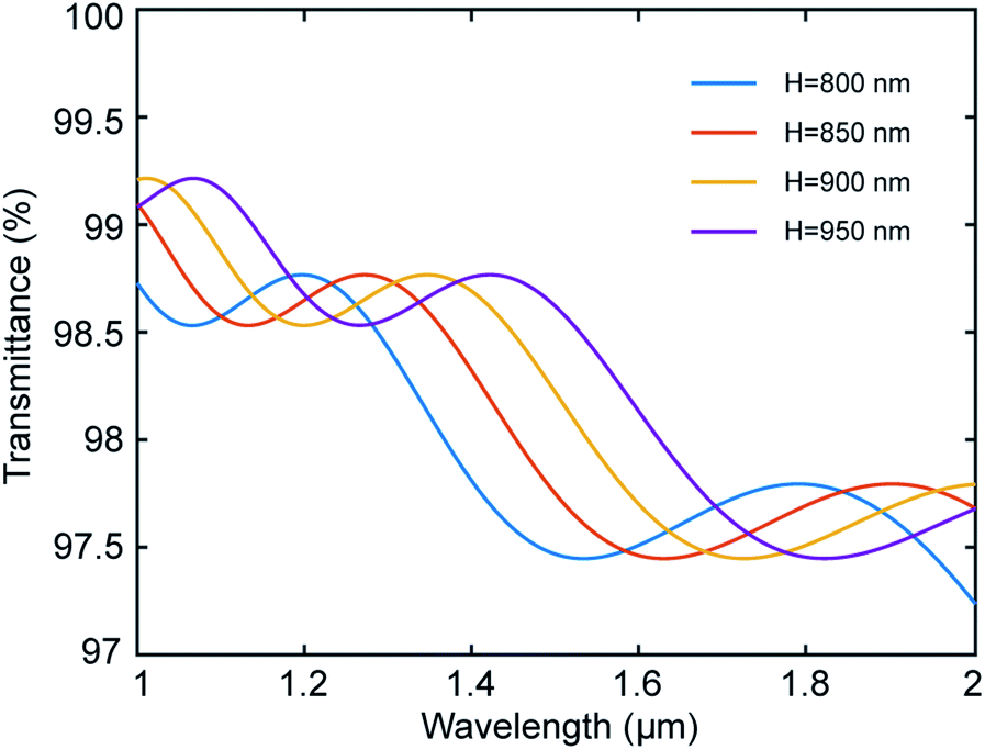
Fig. 8a shows a comparison of the transmittance as a function of wavelength. The diameter of the truncated cones is 450 nm and the depth is varied from H = 800 nm to H = 950 nm in steps of 50 nm. As expected from Babinet's principle, the calculated results are very close to those shown in Fig. 4a, obtained for the extruded features. The transmission drops for longer wavelengths since H becomes shorter in terms of wavelength at these regions. The decrease in transmission can also be seen in Fig. 2, where we simulated a plane-wave incident on an infinite gradient index layer. The lower transmittance can be attributed to several factors, such as unit cell size and discontinuity in the refractive index. The size of the unit-cells is not small enough for the structure to operate in shorter wavelengths due to the large refractive index of the waveguide core material (silicon in our case). Also, the effective refractive index is not continuous at the air-metasurface interface and at the metasurface-waveguide core interface, since the filling factor in cone structures cannot reach 100% with round features.
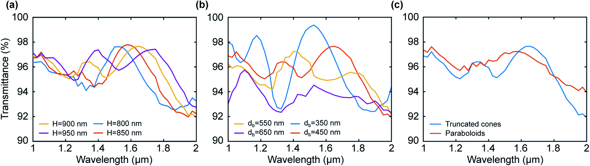 | ||
| Fig. 8 (a) Transmission as a function of wavelength for an hexagonal grid of inverted cones carved on a waveguide facet. The inverted cone has a base diameter of db = 450 nm, an upper radius of du = 200 nm and the depth H varies from 800 nm to 950 nm in steps of 50 nm. (b) Transmission as a function of wavelength for the hexagonal grid depth of H = 900 nm, an upper radius of du = 200 nm; the base radius db varies from 350 nm to 650 nm in steps of 100 nm. (c) Transmission as a function of wavelength for an hexagonal grid. The blue line represents an array of truncated cones with a base radius of db = 450 nm, a top radius of du = 200 nm and a depth of H = 900 nm. The red line represents an array of paraboloids with a bottom radius of db = 450 nm, and a depth of H = 900 nm. | ||
Next, we compare the effect of the unit-cell size in Fig. 8b. Here, we consider the depth of the cones as a constant value of 900 nm and vary the base diameters for values of db = 350, 450, 550, and 650 nm. As expected, the shorter wavelengths region shows higher transmission as the structure approaches the sub-wavelength regime. However, the results for db = 350 nm also exhibit stronger resonant behavior due to the increase in the effective index at the interfaces. Even though a unit-cell size of db = 350 nm can increase transmission by up to 99.4%, one can achieve transmission above 95% over a spectral range of 1–1.8 μm by increasing the unit cell by up to db = 450 nm.
Now, we compare the truncated cone holes with a diameter of db = 450 nm and height of H = 900 nm, to paraboloids with the same depth and base diameter. Fig. 8c shows the result of this comparison. We note that the AR structure on a facet made of paraboloids exhibits less resonant behavior, due to the continuity of the effective index at the tip of the metasurface. By using a parabolic array of holes one can achieve transmission of more than 94% over the entire spectral range of 1–2 μm.
4 Conclusions
To conclude, we demonstrated the transparency effect in optical waveguides. For this, we developed a semi-analytical formalism to predict the metasurface parameters made of high-index dielectric materials, to be engraved on optical waveguides facets. Our proof of principle calculations show that the waveguide with a cone-shape and parabolic tip-shape unit-cell of the metasurface exhibits transmission as high as 98.5%, compared to 70% transmission from the blank waveguide. We noticed that for the conical metasurface with parabolic tip, the transmission and reflections become uniform in the broad spectral range. Importantly, the silicon nanoparticle tip-shape influences the far-field scattering patterns. Engraved-on-facet silicon metasurface of hemispherical tip shape experiences a strong forward scattering effect making them more transparent, as compared to the metasurface of truncated tip shape. Finally, based on Babinet's principle, we proposed that inverted tips – i.e. implementing air-filled unit-cell shapes – should exhibit similar behavior. Indeed, the results for inverted tips are, although not identical, but similar to those of non-inverted shapes. Even though theoretically, deeper holes would improve the transmission through the facet, in practice the depth of the holes is limited fabrication limited and should be approximately twice the base-diameter. Engraved features are also more preferable in terms of fabrication as compared to challenging extruded features. Our results show a broadband transparency effect on a chip and may generate a new class of devices spanning a broad range of applications.Conflicts of interest
There are no conflicts to declare.Acknowledgements
This work has been funded by the Israel Innovation Authority-KAMIN Program, Grant No. 62045. E. F. acknowledges the help of Aviad Katiyi in the preparation of the figures.Notes and references
- A. Karabchevsky, A. Katiyi, A. S. Ang and A. Hazan, Nanophotonics, 2020, 1–24 Search PubMed.
- A. Karabchevsky, A. Katiyi, M. I. M. Bin Abdul Khudus and A. V. Kavokin, ACS Photonics, 2018, 5, 2200–2207 CrossRef CAS.
- A. Karabchevsky, J. S. Wilkinson and M. N. Zervas, Opt. Express, 2015, 23, 14407–14423 CrossRef CAS PubMed.
- A. Karabchevsky and A. Kavokin, Sci. Rep., 2016, 6, 21201 CrossRef CAS PubMed.
- A. Katiyi and A. Karabchevsky, J. Lightwave Technol., 2017, 35, 2902–2908 CAS.
- Y. Galutin, E. Falek and A. Karabchevsky, Sci. Rep., 2017, 7, 12076 CrossRef PubMed.
- P. Cheben, R. Halir, J. H. Schmid, H. A. Atwater and D. R. Smith, Nature, 2018, 560, 565 CrossRef CAS PubMed.
- E. Ash, C. Pitt and M. Wilson, Nature, 1976, 261, 377–381 CrossRef CAS.
- A. Katiyi and A. Karabchevsky, ACS Sens., 2018, 3, 618–623 CrossRef CAS PubMed.
- Z. Wang, A. Abbasi, U. Dave, A. De Groote, S. Kumari, B. Kunert, C. Merckling, M. Pantouvaki, Y. Shi and B. Tian, et al. , Laser Photonics Rev., 2017, 11, 1700063 CrossRef.
- J. Midwinter, Nature, 1976, 261, 371 CrossRef CAS.
- T. Ma, Q. Huang, H. He, Y. Zhao, X. Lin and Y. Lu, Opt. Express, 2019, 27, 16624–16634 CrossRef CAS PubMed.
- W. Cai, Y. Fan, X. Huang, Q. Fu, R. Yang, W. Zhu and F. Zhang, Phys. Rev. A, 2019, 100, 053804 CrossRef CAS.
- J. Hu, T. Lang, Z. Hong, C. Shen and G. Shi, J. Lightwave Technol., 2018, 36, 2083–2093 CAS.
- P. Terekhov, H. Shamkhi, E. Gurvitz, K. Baryshnikova, A. Evlyukhin, A. Shalin and A. Karabchevsky, Opt. Express, 2019, 27, 10924–10935 CrossRef CAS PubMed.
- M. Motamedi, W. H. Southwell and W. J. Gunning, Appl. Opt., 1992, 31, 4371–4376 CrossRef CAS PubMed.
- U. Schallenberg, Advances in Optical Thin Films III, 2008, p. 710103 Search PubMed.
- S. Buddhiraju and S. Fan, Phys. Rev. B, 2017, 96, 035304 CrossRef.
- E. Garnett and P. Yang, Nano Lett., 2010, 10, 1082–1087 CrossRef CAS PubMed.
- N. Yamada, O. N. Kim, T. Tokimitsu, Y. Nakai and H. Masuda, Prog. Photovoltaics, 2011, 19, 134–140 CAS.
- S. Ji, K. Song, T. B. Nguyen, N. Kim and H. Lim, ACS Appl. Mater. Interfaces, 2013, 5, 10731–10737 CrossRef CAS PubMed.
- H. K. Raut, V. A. Ganesh, A. S. Nair and S. Ramakrishna, Energy Environ. Sci., 2011, 4, 3779–3804 RSC.
- M. Keshavarz Hedayati and M. Elbahri, Materials, 2016, 9, 497 CrossRef PubMed.
- U. B. Schallenberg, Advances in Optical Thin Films IV, 2011, p. 81681N Search PubMed.
- P. D. Terekhov, K. V. Baryshnikova, A. S. Shalin, A. Karabchevsky and A. B. Evlyukhin, Opt. Lett., 2017, 42, 835–838 CrossRef PubMed.
- P. D. Terekhov, K. V. Baryshnikova, Y. A. Artemyev, A. Karabchevsky, A. S. Shalin and A. B. Evlyukhin, Phys. Rev. B, 2017, 96, 035443 CrossRef.
- Y. F. Yu, A. Y. Zhu, R. Paniagua-Domínguez, Y. H. Fu, B. Luk'yanchuk and A. I. Kuznetsov, Laser Photonics Rev., 2015, 9, 412–418 CrossRef CAS.
- B. S. Luk'yanchuk, N. V. Voshchinnikov, R. Paniagua-Domínguez and A. I. Kuznetsov, ACS Photonics, 2015, 2, 993–999 CrossRef.
- M. I. Shalaev, J. Sun, A. Tsukernik, A. Pandey, K. Nikolskiy and N. M. Litchinitser, Nano Lett., 2015, 15, 6261–6266 CrossRef CAS PubMed.
- K. Baryshnikova, M. Petrov, V. Babicheva and P. Belov, Sci. Rep., 2016, 6, 22136 CrossRef CAS PubMed.
- H. Yang, G. Li, G. Cao, Z. Zhao, J. Chen, K. Ou, X. Chen and W. Lu, Opt. Express, 2018, 26, 5632–5643 CrossRef CAS PubMed.
- X. Jing, J. Ma, S. Liu, Y. Jin, H. He, J. Shao and Z. Fan, Opt. Express, 2009, 17, 16119–16134 CrossRef CAS PubMed.
- A. Deinega, I. Valuev, B. Potapkin and Y. Lozovik, J. Opt. Soc. Am. A, 2011, 28, 770–777 CrossRef PubMed.
- S. Narayanan, Bell Syst. Tech. J., 1967, 46, 991–1024 CrossRef.
- W. H. Southwell, J. Opt. Soc. Am. A, 1991, 8, 549–553 CrossRef CAS.
- D. S. Hobbs, B. D. MacLeod and J. R. Riccobono, Window and Dome Technologies and Materials X, 2007, p. 65450Y Search PubMed.
- Y. A. Xi, L. Tsakalakos, B. A. Korevaar, T. R. Tolliver and D. Zhong, Nanostructured anti-reflection coatings and associated methods and devices, US Pat. App. 12/421,101, 2010.
- J. Buencuerpo, L. Torne, R. Alvaro, J. M. Llorens, M. L. Dotor and J. M. Ripalda, AIP Conf. Proc., 2017, 030002 CrossRef.
- C. C. Katsidis and D. I. Siapkas, Appl. Opt., 2002, 41, 3978–3987 CrossRef PubMed.
- D. Smith, E. Shiles, M. Inokuti and E. Palik, Handbook of Optical Constants of Solids, 1985, vol. 1, pp. 369–406 Search PubMed.
- I. Malitson, J. Opt. Soc. Am., 1965, 55, 1205–1209 CrossRef CAS.
- M. Born and E. Wolf, Principles of Optics: Electromagnetic Theory of Propagation, Interference, and Diffraction of Light, Press Syndicate of the University of Cambridge, United Kingdom, 1999, p. 461 Search PubMed.
| This journal is © The Royal Society of Chemistry 2020 |