
 Open Access Article
 This Open Access Article is licensed under a
 Creative Commons Attribution 3.0 Unported Licence
Solution-mediated nanometric growth of α-Fe2O3 with electrocatalytic activity for water oxidation†
Asako
Taniguchi
 *ab,
Yuta
Kubota
c,
Nobuhiro
Matsushita
c,
Kento
Ishii
b and
Tetsuo
Uchikoshi
b
*ab,
Yuta
Kubota
c,
Nobuhiro
Matsushita
c,
Kento
Ishii
b and
Tetsuo
Uchikoshi
b
aGraduate School of Pure and Applied Sciences, University of Tsukuba, 1-1-1 Tennodai, Tsukuba, Ibaraki 305-8573, Japan. E-mail: s1930108@s.tsukuba.ac.jp
bResearch Center for Functional Materials, National Institute for Materials Science (NIMS), 1-2-1 Sengen, Tsukuba, Ibaraki 305-0047, Japan
cDepartment of Materials Science and Engineering, School of Materials and Chemical Technology, Tokyo Institute of Technology, 2-12-1 Ookayama, Meguro-ku, Tokyo 152-8550, Japan
First published on 20th July 2020
Abstract
This paper describes a simple, low-temperature, and environmentally friendly aqueous route for the layer-by-layer nanometric growth of crystalline α-Fe2O3. The formation mechanism involves alternative sequences of the electrostatic adsorption of Fe2+ ions on the surface and the subsequent onsite oxidation to Fe3+. A combination analysis of X-ray diffraction, scanning electron microscopy, UV-Vis spectroscopy, and X-ray photoelectron spectroscopy revealed that α-Fe2O3 is directly formed without post-growth annealing via designed chemical reactions with a growth rate of ca. 1.7 nm per deposition cycle. The obtained α-Fe2O3 layer exhibits electrocatalytic activity for water oxidation and, at the same time, insignificant photo-electrocatalytic response, indicating its defective nature. The electrocatalytic activity was tailored by annealing up to 500 °C in air, where thermal diffusion of Sn4+ into the α-Fe2O3 lattice from the substrate probably provides an increased electrical conductivity. The subsequent surface-modification with Ni(OH)2 lowers the overpotential (250 mV at 0.5 mA cm−2) in a 1 M KOH solution. These findings open direct growth pathways to functional metal oxide nanolayers via liquid phase atomic layer deposition.
Introduction
Ceramics coating is a core technology that affords various functions to a substrate material. Metal oxides are particularly attractive for applications in anticorrosion,1 catalysis,2 sensing,3 energy storage4 and conversion,5 optics,6 and electronics.7 In an industry context, oxide materials are deposited by vacuum phase deposition techniques such as chemical vapor deposition,8 pulsed laser deposition,9 and sputtering.10 Solution deposition techniques such as sol–gel,11 electrodeposition,12 and chemical bath-deposition (CBD) methods13 are potential alternatives to the above-mentioned vacuum processes as they utilize inexpensive and less toxic solution precursors as well as ambient pressure for oxide deposition, hence making the fabrication more environmentally friendly and more cost-effective.Moreover, a solution process enables the direct deposition of crystalline oxides on the substrate without post-growth annealing. Low-temperature direct deposition is suitable for film formation on low heat-resistant substrates, expanding the potential scope of functional oxide materials as a component in flexible plastic devices and electrochemical devices with indium-tin-oxide substrates. Recent efforts have allowed the fabrication of various oxide (e.g., ZnO,14 TiO2,15 WO3,16 and SnO2 (ref. 17)) via aqueous solution routes without the need for a post-annealing treatment. However, so far, the direct solution routes have been adopted for tiny members in the broad family of metal oxides. The major difficulty lies in the growth mechanism; according to classical aqueous chemistry, the metallic ions (Mn+) in an aqueous solution react with OH− to precipitate hydroxide nucleus on the substrate via a heterogenous nucleation process (1):18
| Mn+ + nOH− → M(OH)n | (1) |
If the stability of hydroxide is sufficiently low for dehydration, the hydroxide spontaneously transforms into an oxide form during deposition (2):18
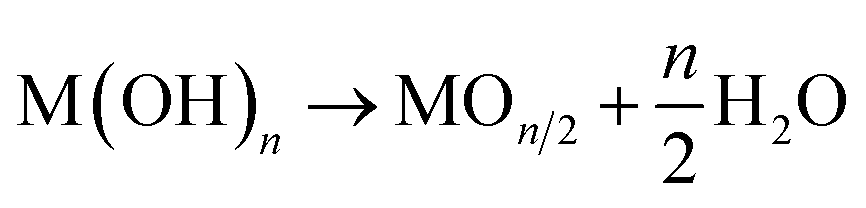 | (2) |
However, hydroxides are often stable so that a post-annealing treatment is inevitable for oxide formation. For example, annealing temperatures over 500 °C are necessary to yield Al2O3 (ref. 19) and ZrO2 (ref. 20) from the hydroxides.
This difficulty also applies to α-Fe2O3, the target material in the present study. Resultant products from classical precipitation reactions between ferric or ferrous precursors with an aqueous base are α-FeOOH, β-FeOOH, γ-FeOOH, σ-FeOOH, and Fe5OH8·4H2O,21–23 while one can find no direct solution route to α-Fe2O3. Nevertheless, Fe3O4 (magnetite) can be formed via a co-precipitation process of ferric and ferrous precursors, even at room temperature.21 In other words, Fe–(OH)2–Fe bonds can preferentially convert Fe–O–Fe bonding via dehydration in an aqueous solution, opening the possibility for direct solution deposition of crystalline α-Fe2O3 under suitable reaction conditions. In fact, using the above idea, we recently developed a liquid phase atomic layer deposition (LP-ALD) of α-Fe2O3via an onsite oxidation and dehydration pathway by using a spin spray technique.24 In this method, a source solution containing Fe2+ and an oxidizing solution containing an oxidizer, NaNO2, was simultaneously sprayed onto the substrates mounted on a rotating table heated to 95 °C. We propose that the deposition mechanism involved alternative sequences of the absorption of Fe2+ ions onto the surface and the subsequent formation of Fe3+–oxygen bonds through reactions with the source and oxidizing solutions, respectively (Fig. 1a). We refer to this deposition process as LP-ALD. Such a non-classical LP-ALD strategy may open direct growth pathways to functional metal oxide nanolayers via aqueous solution chemistry. However, the spin spray technique is available only in the specialized laboratories.
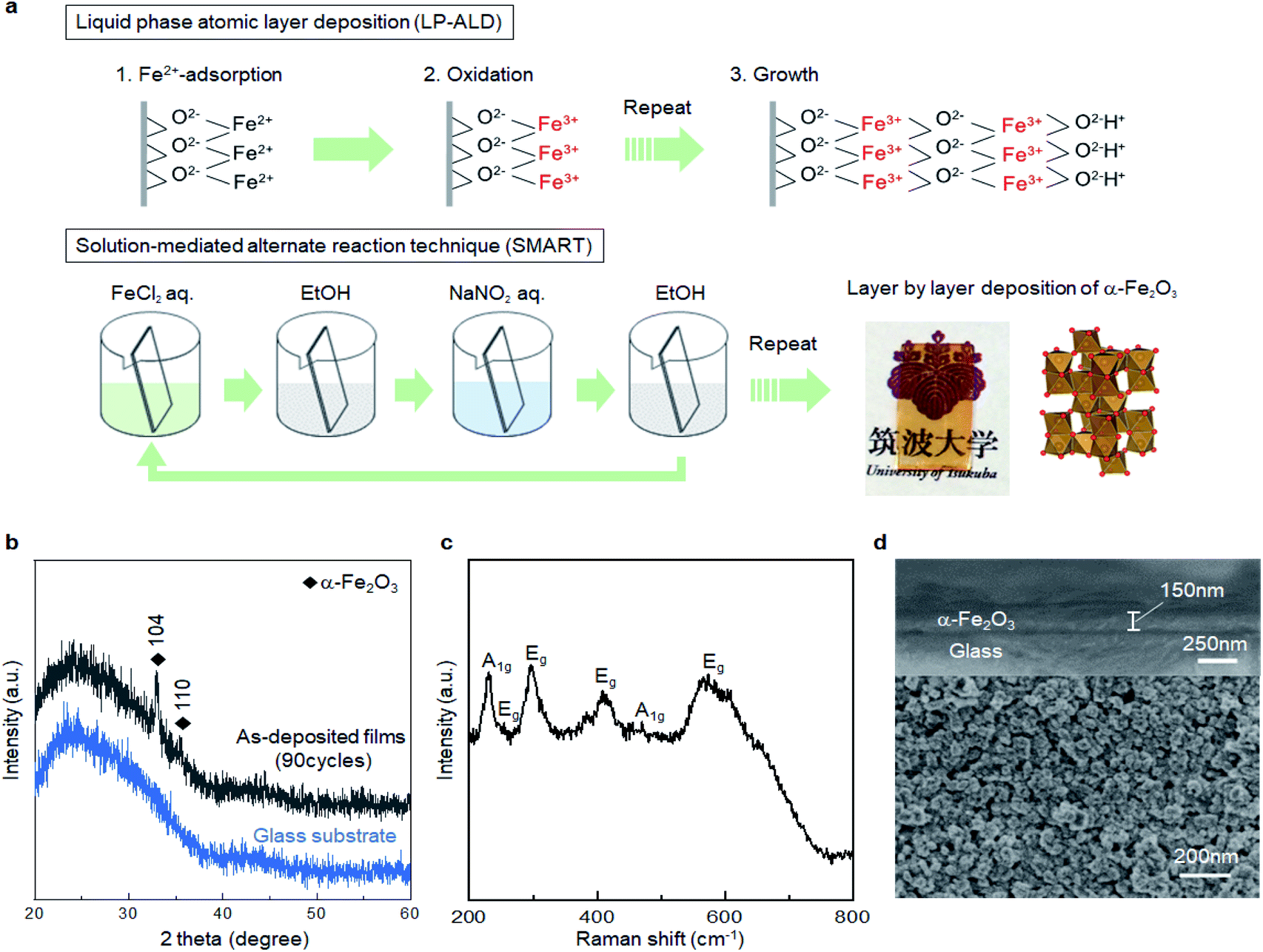 | ||
| Fig. 1 (a) The proposed mechanism of the liquid phase atomic layer deposition (LP-ALD), and the procedure and concept of solution-mediated alternate reaction technique (SMART). (b) XRD pattern, (c) Raman spectrum, and (d) cross-section and surface SEM images of SMART-derived α-Fe2O3 on a glass substrate deposited after 90 cycles. | ||
In the present study, we explore a solution-mediated alternate reaction technique, SMART, to further verify, simplify, and generalize the non-classical LP-ALD reaction pathway (Fig. 1a). Briefly, film deposition in SMART proceeds simply by alternate immersion of the substrate in FeCl2 and NaNO2 precursor solutions. We demonstrate a primitive beaker process that allows the direct growth of crystalline α-Fe2O3 films with a growth rate of ca. 1.7 nm per cycle. Resultant α-Fe2O3 thin films exhibit unexpected electrocatalytic activity for oxygen evolution reactions (OER). The origin of catalytic activity comes from the defective nature of SMART-derived α-Fe2O3 where OH− species are present in the oxide lattice. Sn4+-diffusion into the α-Fe2O3 lattice by annealing and surface modification with Ni(OH)2 further enhance the OER activity, which is superior to state of the art α-Fe2O3-based catalysts.
Experimental section
Preparation of the source and oxidizing solutions
FeCl2·4H2O (Wako Pure Chemical Industries, Ltd., Japan) was used as the metal source precursor. The source solution was prepared by dissolving 20 mM of FeCl2·4H2O in 50 mL of distilled water. The oxidizing solution was prepared by dissolving 20 mM of sodium nitrite (NaNO2, Wako Pure Chemical Industries Ltd., Japan) in 50 mL of distilled water. Nitrogen gas was purged into the solutions at a rate of 1.0 L min−1 while stirring in order to prevent the oxidation of the reactants in the solution.Deposition process in SMART
A soda-lime glass substrate (25 mm × 25 mm × 1 mm) and a transparent conductive oxide (TCO) coated glass substrate (FTO/ITO, Type-0052, 10 Ω sq−1, Geomatec Co., Ltd.) were cleaned in an ultrasonic bath with distilled water, ethanol, and acetone for 10 min each. The glass substrate was further cleaned by treatment in a bath of methanol (Wako Pure Chemical Industries)/HCl (Wako Pure Chemical Industries) (1/1 in volume) for 1 day to obtain a hydrophilic surface, while the TCO substrate was immersed in the 0.1 M HCl (Wako Pure Chemical Industries) for 1 day to obtain a hydrophilic surface.The surface-modified substrate was first immersed in the source solution heated to 75 °C for 1 min, followed by rinsing with ethanol. Then the substrate was immersed in the oxidizing solution heated at 75 °C for 1 min and rinsed with ethanol again. A series of these operations was repeated from 1 to 90 times to control the film thickness.
Ni(OH)2 surface-modification
α-Fe2O3 layer deposited on TCO was immersed in 0.1 M Ni(NO3)2 aqueous solution (Wako Pure Chemical Industries, Ltd., Japan) for 1 min without heating followed by rinsing with water. Then, the substrate was immersed in 1 M KOH solution without heating for 1 min, and then rinsed with water.Fabrication of Ni(OH)2 layer by a successive ionic layer adsorption and reaction (SILAR)
The surface-modified substrate was first immersed in a 0.1 M Ni(NO3)2 aqueous solution heated to 75 °C for 1 min, followed by rinsing with water. Then the substrate was immersed in a 1 M KOH aqueous solution heated at 75 °C for 1 min and rinsed with water. The process was repeated 30 times to obtain Ni(OH)2 layer.Characterization
The crystalline phases of the deposited films were identified by X-ray diffraction (XRD, MultiFlex, Cu Kα, 40 kV and 40 mA, Rigaku). The surface morphologies and textures of the films were observed using a scanning electron microscope (SEM, SU-8020, Hitachi High-Technologies). The elemental distribution was observed an energy dispersive X-ray spectroscopy (EDS, JEOL, JSM-7600). The light absorbance of samples in the ultraviolet-visible (UV-Vis) region was evaluated by the visible absorption spectroscopy (UV-Vis, UV-1280, Shimadzu). X-ray photoelectron spectroscopy (XPS, JPS 9010 TR, JEOL) was conducted to investigate the chemical state of the samples. All measured XPS spectra were calibrated corresponding to the value of the C 1s peak at 284.4 eV using Mg Kα X-ray source with 1253.6 eV. Raman spectroscopy measurements were made LabRam Armis, Horiba Jobin Yvon instrument equipped with 532 nm laser and a microscope to focus the laser light on the film surface.Electrochemical and photoelectrochemical measurements
The OER measurements were performed in 1 M KOH aqueous solution using a three-electrode configuration, with a Pt wire counter electrode and an Ag/AgCl, KCl reference electrode. All potentials have been referenced to the reversible hydrogen electrode (RHE) by the expression: VRHE = VAg/AgCl + 0.197 V + 0.059 V × pH. The linear sweep voltammograms (LSV) was performed for 20 cycles with a scan rate of 5 mV s−1. Photoelectrochemical measurements were performed at the same condition, while visible light (wavelength above 400 nm) was irradiated for the measurements. The 200 W Xeon lamp (Asahi Spectra. Co) was used for the measurements.Results and discussion
Characterization of SMART-derived thin films
The reaction pathway of SMART is designed as follows. In the first step, the substrate is immersed in a FeCl2 solution with pH 4 to form a Fe2+ adlayer onto the substrate surface. When an oxide surface is negatively charged at the pH, a double layer is formed on the surface where Fe2+ forms an inner layer (Stern layer) and the Cl− from the FeCl2 precursor forms a charge-balancing outer layer. In the following step, the substrate is rinsed with ethanol so that only the immobile double-layer remains on the substrate surface. Subsequently, the substrate is immersed in the NaNO2 solution and heated to 75 °C. The NO2− in the solution is diffused onto the surface to oxidize the adsorbed Fe2+ to the Fe3+ state. At this stage, hydrolysis and dehydration simultaneously occur onsite, resulting in the formation of the first O–Fe–O bonds. In a final step, the substrate is rinsed again to remove the ions from the diffusion layer. In principle, the repletion of these cycles leads to a layer-by-layer deposition of the α-Fe2O3 layer.Fig. 1b shows the X-ray diffraction pattern from the sample prepared by the SMART on the glass substrate after 90 cycles of deposition. The pattern displays broad peaks from the glass substrate and sharp peaks corresponding to 104 and 110 reflections of the α-Fe2O3 phase (JCPDS 33-0664) without an impurity phase such as Fe(OH)2, Fe(OH)3, FeOOH, Fe3O4, and γ-Fe2O3. According to Scherrer's equation using a 104 peak, the crystallite size is calculated to be 47.4 nm.25 Raman spectroscopy was employed to further investigate the phase purity of the resultant films. As shown in Fig. 1c, all the detected peaks are assigned as two A1g modes (231 and 473 cm−1) and four Eg modes (255, 297, 411, and 576 cm−1),26,27 in support of the film being composed of α-Fe2O3 domains. Note that Raman spectra up to 1400 cm−1 shown in Fig. S1, ESI† also exclude the formation of iron-based impurity phases.28
Fig. 1d displays the cross-sectional and surface SEM images of the SMART-derived α-Fe2O3 film. The cross-sectional image reveals the formation of a dense layer with a relatively uniform thickness of 150 nm on average. Thus, the growth rate can be estimated at approximately 1.7 nm per deposition cycle, if the film thickness linearly increases in each deposition cycle. The surface image presents a continuous film consisting of dense grains with an average size of ca. 50 nm. The grain size roughly matches the calculated crystallite size (47.4 nm) from the XRD pattern, indicating that each grain consists of a single crystalline domain. Indeed, the SEM observation with a lower magnification confirms that the film is free from cracks (Fig. S2, ESI†). Owing to the high uniformity, the film was transparent with a yellowish red color, as shown in the inserted photograph in Fig. 1a. The film exhibited good adhesion to the substrate after scotch tape testing, indicating the presence of chemical bonds at the interface between the substrate and the α-Fe2O3 layer.
Growth rate and mechanism of SMART process
We verify the growth mechanism by monitoring the change of UV-Vis spectra with an increase in the number of deposition cycles. Fig. 2a shows a change in the UV-Vis absorption spectra after 1, 3, 5, 10, 15, 20, 25, and 30 cycles on the glass substrate. In general, the absorption gradually intensified with the number of deposition cycles, while the spectral feature, e.g., absorption onset, was not largely changed after at least 3 cycles, indicating that the α-Fe2O3 layer was deposited throughout the cycles. Fig. 2b displays plots of absorption intensity at 400 nm versus the number of deposition cycles. The plots were fitted with lines at a slope of ca. 0.01 per cycle. Note that the absorption coefficient for 90 cycles of deposited α-Fe2O3 was 1.12 at 400 nm (Fig. S3, ESI†). From this value, the slope was calculated to 0.012 per cycle, which accords well to the slope value obtained from up to 30 cycles. Thus, the UV-Vis absorption data supports that the α-Fe2O3 film is deposited in a layer-by-layer manner. The calculated crystallite size, 47.4 nm from the XRD pattern (Fig. 1b), was 28 times larger than the growth rate (ca. 1.7 nm). Thus, the Fe2+ species in the Stern layer was mainly consumed for crystal growth rather than the heterogeneous nucleation process. We confirm that the slope value that fitted with the UV-Vis data was unchanged when the TCO substrate was used as the substrate (Fig. 2b). This result is reproducible. The thickness of a α-Fe2O3 layer on an TCO was observed to approximately 50 nm after 30 deposition cycles (Fig. S4, ESI†). This further confirms that the growth rate was about 1.7 nm per cycle.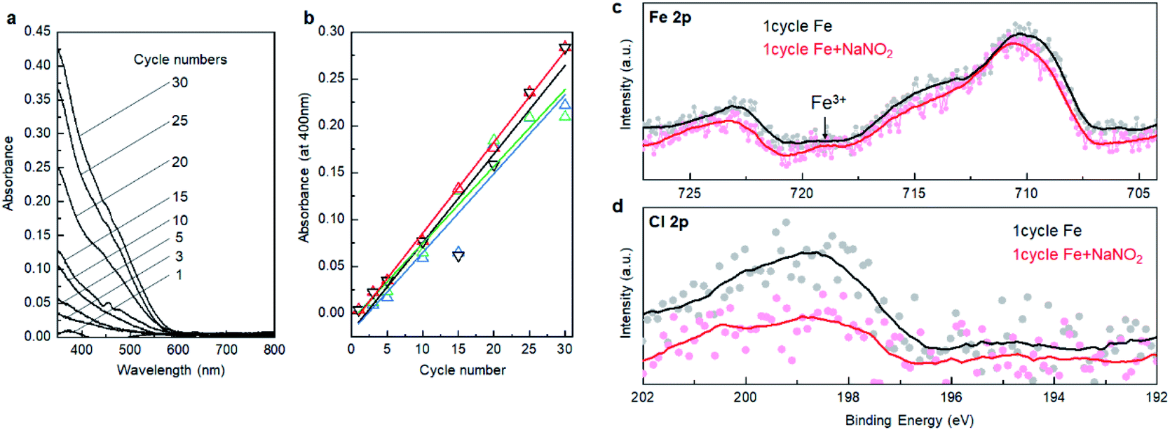 | ||
| Fig. 2 (a) UV-Vis spectra of SMART-derived α-Fe2O3 obtained after 1, 3, 5, 10, 15, 20, 25, and 30 deposition cycles, (b) plots of absorption intensity at 400 nm versus deposition cycles, where the ∇ and Δ symbols denote the plots from the sample deposited on glass and TCO substrates, respectively. (c) Fe 2p and (d) Cl 2p XPS spectra of the deposited layer after the first step (black) and second step (red) in the first deposition cycle. | ||
We employed X-ray photoemission spectroscopy (XPS) to detect the changes in surface states of the first cycle. Fig. 2c displays Fe 2p XPS spectra of the deposited layer after the reaction with FeCl2 followed by the rinse step, and one subsequently reacted with the NaNO2 solution followed by a second rinse step. Note that the Sn 3p3/2 background signal was extracted from the as-obtained data to better understand the Fe 2p spectra see Fig. S5, ESI.† The Fe 2p spectra involve multi-components including Fe 2p1/2, Fe 2p3/2, and their satellite peaks, while it can be quantitively described that the peaks shifted toward the higher energy side after reaction with NaNO2. Indeed, a peak at around 719 eV, attributable to a Fe 2p1/2 satellite of Fe3+, was pronounced after the reaction.29,30 These changes demonstrate that the oxidation of Fe2+ occurred by reactions with the NaNO2 solution. Besides, the intensity of the Cl 2p peak (Fig. 2d) decreased after the second step. This supports the notion that the Cl− ions involved in the outer layer of the double-layer were replaced by O2− or OH− species binding with Fe3+ after the oxidation step. Thus, all the analytical results support that the α-Fe2O3 layer could be deposited, according to the designed SMART concept (Fig. 1a). The direct formation of α-Fe2O3 demonstrates that controlling surface redox reactions in the growth process plays a critical role in crystallization. The idea would be applied to bring intriguing aqueous routes to crystalline metal oxides based on multivalent metallic components such as Cu1+/2+, Co2+/3+, and Mn2+/3+/4+.
Electrocatalytic properties of SMART-derived thin films
Subsequently, we investigated the electrochemical and photo-electrochemical catalytic performance of SMART-derived α-Fe2O3 for an oxygen evolution reaction (OER) to find any structure–performance correlations. As is well known, OER is the essence of renewable fuel generation in water electrolysis, and development of stable, cost-effective, and environmentally-friendly OER catalysts is a key challenge.31–35 This sheds light on α-Fe2O3 as one of the most suitable materials.36,37Fig. 3a shows plots of linear sweep voltammograms (LSV) of a α-Fe2O3 deposited TCO substrate after 30 cycles of SMART along with a bare-TCO reference. In this case, the measurements were performed without light-irradiation. A bare TCO shows a tiny cathodic current (0.18 mA cm−2 at 1.8 V), while a current of more than one order of magnitude higher is gained at the same potential after α-Fe2O3 deposition. The overpotential is about 390 mV at 0.5 mA cm−2.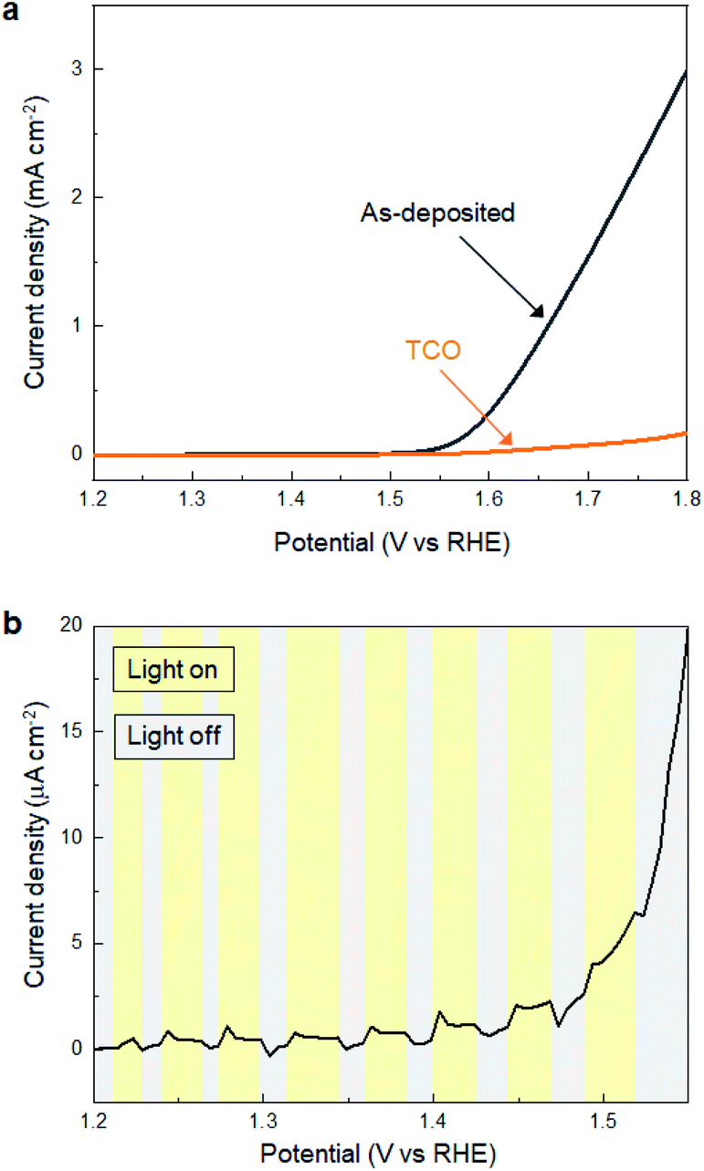 | ||
| Fig. 3 (a) LSV curves for SMART-derived α-Fe2O3 obtained after 30 deposition cycles on an TCO substrate and bare-TCO. (b) The effects of photoirradiation on the current density for SMART-derived α-Fe2O3 obtained after 30 deposition cycles on an TCO substrate. | ||
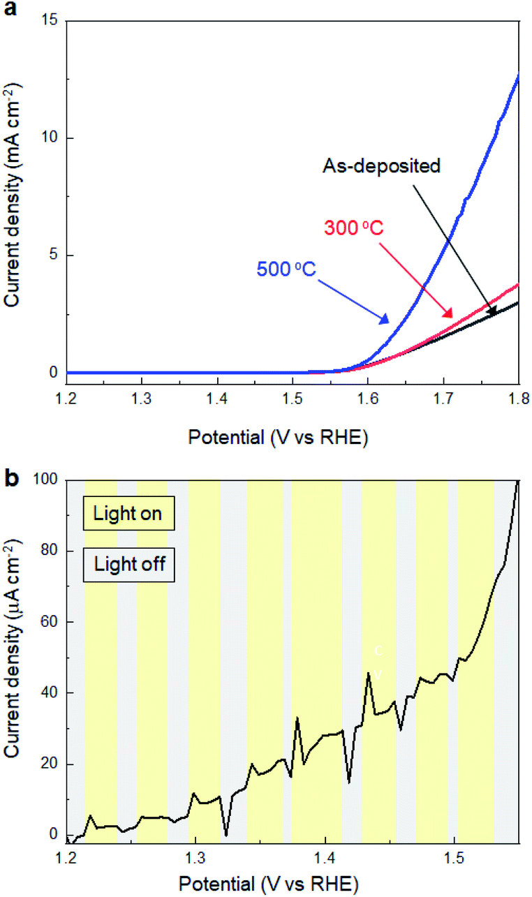
We also performed electrochemical measurements under light-irradiation to investigate catalytic activity of photo-electrochemical water oxidation (Fig. 3b). As a result, a tiny increase of cathodic current in the μA cm−2 range was observed, which demonstrates that most photogenerated electron/hole pairs were expensed for the recombination pathways rather than for water oxidation. To our knowledge, there has been no report of α-Fe2O3-based materials simultaneously exhibiting good electrocatalytic activity (measured without light-irradiation) and photo-electrocatalytic activity (measured with light-irradiation) for water oxidation. This is most probably because they are in a trade-off relationship; namely, defects increase the electron conductivity required for the former catalysis, while they induce recombination pathways for the photogenerated carriers that are avoided for the latter. Considering that SMART was conducted at a low temperature of 75 °C, a SMART-derived α-Fe2O3 layer would be more defective than those synthesized by high-temperature methods, which could be the main reason for the remarkable catalytic activity of SMART-derived α-Fe2O3.
Subsequently, we investigated the effects of thermal annealing in air on the electrochemical properties of SMART-derived α-Fe2O3 to understand the correlation between the catalytic activity and local structures in α-Fe2O3 layers. Fig. 4a shows the LSV curves of the SMART-derived α-Fe2O3 layer, as-deposited and subsequently annealed at 300 °C and 500 °C. After annealing at 300 °C, the cathodic current density increased slightly. The catalytic activity was significantly enhanced with the overpotential of 370 mV at 0.5 mA cm−2 after annealing at 500 °C. We assumed that the activity would decrease after the annealing in air due to the elimination of defects. However, the trend of the experimental results was the opposite of our expectations, indicating that the α-Fe2O3 layer remained defective after annealing. In fact, the photo-response remained negligible after annealing at 500 °C (Fig. 4b).
 | ||
| Fig. 4 (a) LSV curves for SMART-derived α-Fe2O3 obtained after 30 deposition cycles on an TCO substrate; as-deposited, and subsequently annealed at 300 °C and 500 °C. (b) The effects of photoirradiation on the current density for SMART-derived α-Fe2O3 obtained after 30 deposition cycles on an TCO substrate (annealed 500 °C). | ||
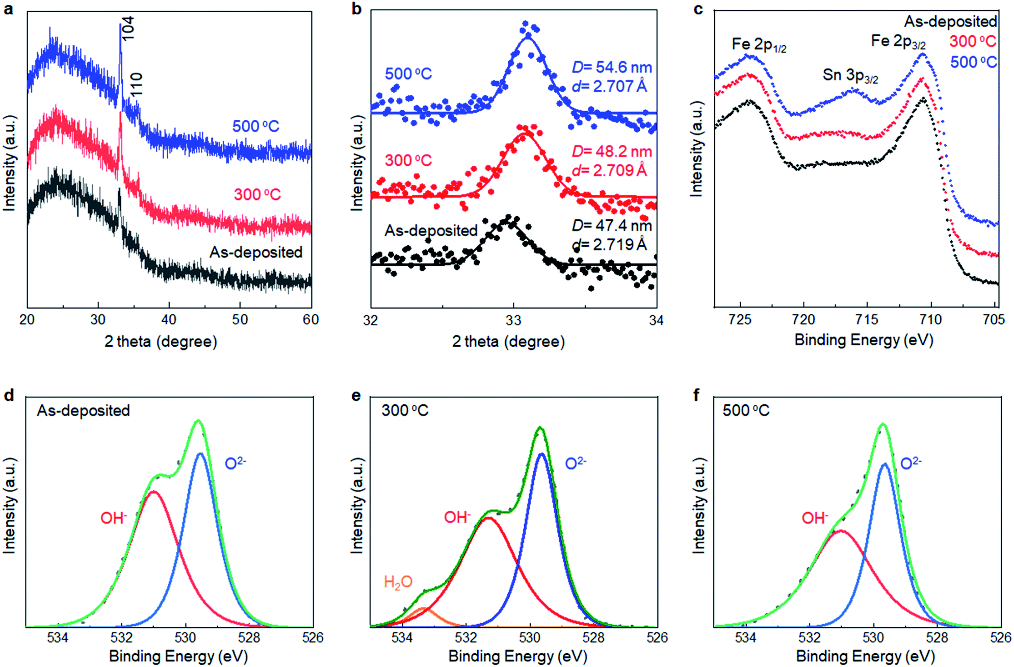
XRD analyses were performed to collect information about the local structure changes of α-Fe2O3 layers after annealing (Fig. 5a and b). First, no additional peaks emerged after annealing up to 500 °C, supporting that the as-deposited films were mainly composed of crystalline α-Fe2O3. Second, the average crystallite size slightly increased to 54.6 nm from 47.4 nm after annealing at 500 °C. Third, the d-value calculated from the 104 peak position corresponded to 2.719 Å, 2.709 Å, and 2.707 Å for the as-deposited film and ones subsequently annealed at 300 °C and 500 °C, respectively, while the d-value obtained from a reference bulk crystalline α-Fe2O3 was 2.703 Å (Fig. S6, ESI†). Thus, the lattice expansion occurred in as-deposited α-Fe2O3, and the lattice shrank to the bulk value after the annealing.
 | ||
| Fig. 5 (a) Total and (b) Selected angle XRD patterns of the SMART-derived α-Fe2O3 deposited on a glass substrate. (c) Fe 2p XPS spectra of the SMART-derived α-Fe2O3 deposited on an TCO substrate, as-deposited, and subsequently annealed at 300 °C and 500 °C. O 1s XPS spectra of the SMART-derived α-Fe2O3 deposited on an TCO substrate, (d) as-deposited, and subsequently annealed at (e) 300 °C and (f) 500 °C. | ||
XPS was performed to detect the change in chemical states of the α-Fe2O3 after annealing. Fig. 5c–f show Fe 2p and O 1s spectra of SMART-derived α-Fe2O3 with and without annealing at 300 °C and 500 °C. In the Fe 2p spectra, a Sn 3p3/2 peak located at 716 eV appeared after annealing at 500 °C. It was also found that Sn 3d peaks in the wide-scan spectrum were pronounced after the annealing (Fig. S7, ESI†). Thus, Sn4+ ions, involved in the conducting substrate, would be thermally diffused in the α-Fe2O3 lattice. In fact, this phenomenon can be found in the literatures.38–40 Sn4+ exhibits a similar ionic radius and Pauling electronegativity to Fe3+ ions, which facilitates the substitution of Fe3+ to Sn4+ in α-Fe2O3. Importantly, Sn4+-doping has been found to be an effective approach for tailoring the electronic properties of α-Fe2O3.41–43 In the present case, the catalytic activity was likely enhanced by an increased electron conductivity by Sn4+-doping.43 Two binding energies of O 1s (529.5 eV and 531.0 eV) were assigned to the O2− and OH−, respectively.44,45 The ratio of OH−/O2− decreased after annealing at 300 °C. Thus, we suggest that the observed lattice expansion in the as-deposited α-Fe2O3 layer was caused by the OH species.46,47 Finally, the intensity of the Cl 2p was quite weak in the as-deposited sample. The peak was almost undetectable after annealing at 300 °C, excluding the significant contributions of Cl− to change the catalytic activity upon annealing (Fig. S8, ESI†).
Enhanced catalytic activity at Ni(OH)2/α-Fe2O3 heterointerface
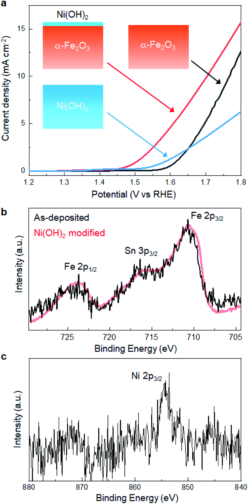
We revealed that defect-engineering by annealing is effective in enhancing the electrocatalytic activity of α-Fe2O3. Here, we further extended the LP-ALD concept to tailor the catalytic activity, where the Ni(OH)2 layer was decorated onto the surface of the α-Fe2O3 film after annealing at 500 °C. The Ni(OH)2 layer was deposited SILAR method,18,48 referred to as the most relevant deposition technique to SMART. In SILAR, metal ions were adsorbed onto the surface followed by rinsing with water. In the next step, metal cations reacted with an alkaline solution to form a metal hydroxide layer via classical precipitation reactions (eqn (1)). In fact, this attempt significantly improved the OER activity; as shown in Fig. 6a, the overpotential was lowered to 250 mV at 0.5 mA cm−2 after the Ni(OH)2-modification. The overpotential at the same current density was ca. 50 mV lower than those from the best α-Fe2O3-based catalysts, Ni- or Zn-doped α-Fe2O3, reported so far.36 No degradation of catalytic performance was observed after 100 scans, which indicated the catalytic durability. The Ni(OH)2-modified α-Fe2O3 showed better catalytic activity than SILAR-derived Ni(OH)2, where the overpotential of a Ni(OH)2 layer obtained after 30 deposition cycles was 320 mV at 0.5 mA cm−2. Fig. 6b and c show the Fe 2p and Ni 2p XPS spectra of Ni(OH)2-modified α-Fe2O3, respectively. There is no remarkable change in the features of the Fe 2p spectra, indicating that the Fe–O–Fe framework containing oxygen vacancies was not altered by Ni(OH)2-modification. Based on the relative peak intensity of the Ni 2p and Fe 2p spectra, the Ni![[thin space (1/6-em)]](https://www.rsc.org/images/entities/char_2009.gif) :Fe atomic ratio is approximately 1:3. Considering the analytical depth of the XPS (ca. 4 nm), the thickness of the Ni(OH)2 layer is estimated to be 1 nm. Besides, SEM-EDX analysis revealed that Ni signal was homogenously detected on the whole surface of the α-Fe2O3 layer, while there was no morphological change on the surface (Fig. S9, ESI†). In addition, no additional reflection peaks from Ni-based phases were detected in the XRD pattern of the Ni(OH)2-modified sample (Fig. S10, ESI†). This indicates that particulate Ni(OH)2 was not formed, while Ni(OH)2 would be uniformly formed on the α-Fe2O3 surface. These results support that catalytic activity was modified through the formation of Ni(OH)2/α-Fe2O3 heterointerface.
:Fe atomic ratio is approximately 1:3. Considering the analytical depth of the XPS (ca. 4 nm), the thickness of the Ni(OH)2 layer is estimated to be 1 nm. Besides, SEM-EDX analysis revealed that Ni signal was homogenously detected on the whole surface of the α-Fe2O3 layer, while there was no morphological change on the surface (Fig. S9, ESI†). In addition, no additional reflection peaks from Ni-based phases were detected in the XRD pattern of the Ni(OH)2-modified sample (Fig. S10, ESI†). This indicates that particulate Ni(OH)2 was not formed, while Ni(OH)2 would be uniformly formed on the α-Fe2O3 surface. These results support that catalytic activity was modified through the formation of Ni(OH)2/α-Fe2O3 heterointerface.
 | ||
| Fig. 6 (a) LSV-curves of the SMART-derived α-Fe2O3 (annealed at 500 °C) before/after Ni(OH)2 surface-modification and SILAR-derived Ni(OH)2 (b) Fe 2p and (c) Ni 2p XPS spectra of the SMART-derived α-Fe2O3 (annealed at 500 °C) after Ni(OH)2 surface modification. | ||
Finally, for perspective, we propose that the LP-ALD process could provide a platform to create artificial two-dimensional (2D) heterostructures. 2D heterostructures such as BaTiO3/SrTiO3 superlattice were initially fabricated by a vacuum process,49 and recently, hetero-assembly of 2D nanomaterials such as graphene, as well as 2D transition metal dichalcogenides and 2D oxides have attracted considerable attention for tuning functionalities by interface coupling.50,51 Although LP-ALD, including SILARs and solution-ALD,52 has only been employed for the deposition of inorganic layers with single components, the layer-by-layer deposition principle is applicable to produce such 2D heterostructures. The Ni(OH)2/α-Fe2O3 heterointerface with excellent OER activity, found in the present study, partially demonstrate the above strategy. However, a true understanding of the enhancement of the heterointerface remains challenging because of the complex nature of the surface system, and thus is beyond the scope of this current study. For example, we found that enhancement of OER activity was less significant, when Ni(OH)2 was deposited on the as-deposited α-Fe2O3 layer (Fig. S11, ESI†). Presently, we expect that the periodical 2D heterostructures, such as alternately stacked Ni(OH)2/α-Fe2O3 layers, would serve rich chemistry, affording superior catalytic activity. This will be the target of our next study.
Conclusion
In conclusion, we established SMART for the direct solution deposition of α-Fe2O3 layers on oxide substrates. This method yielded a α-Fe2O3 layer with a 150 nm thickness and a crystalline size of 47.4 nm after 90 deposition cycles. The growth rate was ca. 1.7 nm per deposition cycle, in which Fe2+ cations in a Stern layer were oxidized by NaNO2 to form Fe3+ followed by consumption by crystal growth. Thus, the designed reaction route for the α-Fe2O3 layer was experientially demonstrated. OH− ligands were introduced in the lattice of α-Fe2O3 crystallites, probably because of the low-temperature aqueous process. The defective feature of SMART-derived α-Fe2O3 activated and deactivated electrochemical and photoelectrochemical activity for water oxidation, respectively. The annealing in air introduced the Sn4+ ions in the α-Fe2O3 layer by the thermal diffusion from the substrate, which enhanced the electrocatalytic activity. Finally, we found that Ni(OH)2/α-Fe2O3 heterointerface provided excellent OER activity, which would be crucial to develop stable, cost-effective, and environmentally-friendly OER catalysts.Conflicts of interest
There are no conflicts to declare.Acknowledgements
The authors would like to thank Prof. Yoshikazu Suzuki, Tsukuba University, for fruitful discussion.Notes and references
- T. Tatsuma, S. Saitoh, Y. Ohko and A. Fujishima, Chem. Mater., 2001, 13, 2838–2842 CrossRef CAS.
- R. D. L. Smith, M. S. Prévot, R. D. Fagan, S. Trudel and C. P. Berlinguette, J. Am. Chem. Soc., 2013, 135, 11580–11586 CrossRef CAS.
- S. Zhang, P. Zhang, Y. Wang, Y. Ma, J. Zhong and X. Sun, ACS Appl. Mater. Interfaces, 2014, 6, 14975–14980 CrossRef CAS.
- S. Tong, B. Ma, M. Narayanan, S. Liu, R. Koritala, U. Balachandran and D. Shi, ACS Appl. Mater. Interfaces, 2013, 5, 1474–1480 CrossRef CAS.
- S. Pandya, J. Wilbur, J. Kim, R. Gao, A. Dasgupta, C. Dames and L. W. Martin, Nat. Mater., 2018, 17, 432–438 CrossRef CAS.
- J. Wu, S. Fu, X. Zhang, C. Wu, A. Wang, C. Li, G. Shan and Y. Liu, ACS Appl. Mater. Interfaces, 2020, 12, 6262–6267 CrossRef CAS.
- M.-G. Kim, M. G. Kanatzidis, A. Facchetti and T. J. Marks, Nat. Mater., 2011, 10, 382–388 CrossRef CAS.
- A. M. Alotaibi, S. Sathasivam, B. A. D. Williamson, A. Kafizas, C. Sotelo-Vazquez, A. Taylor, D. O. Scanlon and I. P. Parkin, Chem. Mater., 2018, 30, 1353–1361 CrossRef CAS.
- A. Serrano, J. Rubio-Zuazo, J. López-Sánchez, I. Arnay, E. Salas-Colera and G. R. Castro, J. Phys. Chem. C, 2018, 122, 16042–16047 CrossRef CAS.
- S. Kment, P. Schmuki, Z. Hubicka, L. Machala, R. Kirchgeorg, N. Liu, L. Wang, K. Lee, J. Olejnicek, M. Cada, I. Gregora and R. Zboril, ACS Nano, 2015, 9, 7113–7123 CrossRef CAS.
- Y. Sun, J. H. Seo, C. J. Takacs, J. Seifter and A. J. Heeger, Adv. Mater., 2011, 23, 1679–1683 CrossRef CAS.
- V. M. Guerin, C. Magne, T. Pauporté, T. Le Bahers and J. Rathousky, ACS Appl. Mater. Interfaces, 2010, 2, 3677–3685 CrossRef CAS.
- Z. Shi and A. V. Walker, Langmuir, 2015, 31, 1421–1428 CrossRef CAS.
- S. S. Shin, W. S. Yang, J. H. Noh, J. H. Suk, N. J. Jeon, J. H. Park, J. S. Kim, W. M. Seong and S. I. Seok, Nat. Commun., 2015, 6, 7410 CrossRef CAS.
- A. M. Peiró, J. Peral, C. Domingo, X. Domènech and J. A. Ayllón, Chem. Mater., 2001, 13, 2567–2573 CrossRef.
- T. Stubhan, N. Li, N. A. Luechinger, S. C. Halim, G. J. Matt and C. J. Brabec, Adv. Energy Mater., 2012, 2, 1433–1438 CrossRef CAS.
- N. Shirahata, W. Shin, N. Murayama, A. Hozumi, Y. Yokogawa, T. Kameyama, Y. Masuda and K. Koumoto, Adv. Funct. Mater., 2004, 14, 580–588 CrossRef CAS.
- T. P. Niesen and M. R. De Guire, Solid State Ionics, 2002, 151, 61–68 CrossRef CAS.
- Y. Tokudome, K. Fujita, K. Nakanishi, K. Miura and K. Hirao, Chem. Mater., 2007, 19, 3393–3398 CrossRef CAS.
- S.-m. Chang and R.-a. Doong, Chem. Mater., 2005, 17, 4837–4844 CrossRef CAS.
- A. P. LaGrow, M. O. Besenhard, A. Hodzic, A. Sergides, L. K. Bogart, A. Gavriilidis and N. T. K. Thanh, Nanoscale, 2019, 11, 6620–6628 RSC.
- R. M. Cornell and U. Schwetmann, in The Iron Oxides, 2003, pp. 9–38 Search PubMed.
- B. Li, J. Chen, L. Han, Y. Bai, Q. Fan, C. Wu, X. Wang, M. Lee, H. L. Xin, Z. Han and Y. Yin, Chem. Mater., 2020, 32(7), 3271–3277 CrossRef CAS.
- A. Taniguchi, T. Taniguchi, H. Wagata, K.-i. Katsumata, K. Okada and N. Matsushita, CrystEngComm, 2019, 21, 4184–4191 RSC.
- U. Holzwarth and N. Gibson, Nat. Nanotechnol., 2011, 6, 534 CrossRef CAS.
- I. Chamritski and G. Burns, J. Phys. Chem. B, 2005, 109, 4965–4968 CrossRef CAS.
- D. L. A. de Faria, S. Venâncio Silva and M. T. de Oliveira, J. Raman Spectrosc., 1997, 28, 873–878 CrossRef CAS.
- X. Jiang, Z. Zhang, J. Mei, D. Han, M. Xie, F. Wang, E. Xie and W. Han, Electrochim. Acta, 2018, 273, 208–215 CrossRef CAS.
- E. S. Cho, M. J. Kang and Y. S. Kang, Phys. Chem. Chem. Phys., 2015, 17, 16145–16150 RSC.
- I. Herrmann-Geppert, P. Bogdanoff, J. Radnik, S. Fengler, T. Dittrich and S. Fiechter, Phys. Chem. Chem. Phys., 2013, 15, 1389–1398 RSC.
- Z.-P. Wu, X. F. Lu, S.-Q. Zang and X. W. Lou, Adv. Funct. Mater., 2020, 1910274 CrossRef CAS.
- L. Lv, Z. Yang, K. Chen, C. Wang and Y. Xiong, Adv. Energy Mater., 2019, 9, 1803358 CrossRef.
- Q. Shi, C. Zhu, D. Du and Y. Lin, Chem. Soc. Rev., 2019, 48, 3181–3192 RSC.
- J. M. Gonçalves, M. Ireno da Silva, L. Angnes and K. Araki, J. Mater. Chem. A., 2020, 8, 2171–2206 RSC.
- T. Zhang, Y. Zhu and J. Y. Lee, J. Mater. Chem. A., 2018, 6, 8147–8158 RSC.
- H. C. Nguyën, F. A. Garcés-Pineda, M. de Fez-Febré, J. R. Galán-Mascarós and N. López, Chem. Sci., 2020, 11, 2464–2471 RSC.
- H. Wu, T. Yang, Y. Du, L. Shen and G. W. Ho, Adv. Mater., 2018, 30, 1804341 CrossRef.
- K. Sivula, R. Zboril, F. L. Formal, R. Robert, A. Weidenkaff, J. Tucek, J. Frydrych and M. Grâtzel, J. Am. Chem. Soc., 2010, 132(21), 7436–7444 CrossRef CAS.
- Y. Ling, G. Wang, D. A. Wheeler, J. Z. Zhang and Y. Li, Nano Lett., 2011, 11(5), 2119–2125 CrossRef CAS.
- M. Li, Y. Yang, Y. Ling, W. Qiu, F. Wang, T. Liu, Y. Song, X. Liu, P. Fang, Y. Tong and Y. Li, Nano Lett., 2017, 17, 2490–2495 CrossRef CAS.
- L. Xi, S. Y. Chiam, W. F. Mak, P. D. Tran, J. Barber, S. C. J. Loo and L. H. Wong, Chem. Sci., 2013, 4, 164–169 RSC.
- X. Yang, R. Liu, Y. Lei, P. Li, K. Wang, Z. Zheng and D. Wang, ACS Appl. Mater. Interfaces, 2016, 8, 16476–16485 CrossRef CAS.
- C. M. Tian, W.-W. Li, Y. M. Lin, Z. Z. Yang, L. Wang, Y. G. Du, H. Y. Xiao, L. Qiao, J. Y. Zhang, L. Chen, D.-C. Qi, J. L. MacManus-Driscoll and K. H. L. Zhang, J. Phys. Chem. C, 2020, 124, 12548–12558 CrossRef CAS.
- X.-F. Lu, X.-Y. Chen, W. Zhou, Y.-X. Tong and G.-R. Li, ACS Appl. Mater. Interfaces, 2015, 7, 14843–14850 CrossRef CAS.
- C.-Y. Cao, J. Qu, W.-S. Yan, J.-F. Zhu, Z.-Y. Wu and W.-G. Song, Langmuir, 2012, 28, 4573–4579 CrossRef CAS.
- K. Sohlberg, S. T. Pantelides and S. J. Pennycook, J. Am. Chem. Soc., 2001, 123, 6609–6611 CrossRef CAS.
- A. K. E. Andersson, S. M. Selbach, C. S. Knee and T. Grande, J. Am. Ceram. Soc., 2014, 97, 2654–2661 CrossRef CAS.
- A. J. Abel, A. M. Patel, S. Y. Smolin, B. Opasanont and J. B. Baxter, J. Mater. Chem. A, 2016, 4, 6495–6504 RSC.
- B. Bein, H.-C. Hsing, S. J. Callori, J. Sinsheimer, P. V. Chinta, R. L. Headrick and M. Dawber, Nat. Commun., 2015, 6, 10136 CrossRef CAS.
- A. K. Geim and I. V. Grigorieva, Nature, 2013, 499, 419–425 CrossRef CAS.
- M. Osada and T. Sasaki, Adv. Mater., 2012, 24, 210–228 CrossRef CAS.
- Y. Wu, D. Döhler, M. Barr, E. Oks, M. Wolf, L. Santinacci and J. Bachmann, Nano Lett., 2015, 15, 6379–6385 CrossRef CAS.
Footnote |
| † Electronic supplementary information (ESI) available: SEM images, UV-Vis, XPS spectra, XRD pattern. See DOI: 10.1039/d0na00345j |
| This journal is © The Royal Society of Chemistry 2020 |