
 Open Access Article
 This Open Access Article is licensed under a Creative Commons Attribution-Non Commercial 3.0 Unported Licence
Electro-thermal transport in disordered nanostructures: a modeling perspective
Fabian
Ducry
 *,
Jan
Aeschlimann
and
Mathieu
Luisier
*,
Jan
Aeschlimann
and
Mathieu
Luisier
Integrated Systems Laboratory, ETH Zurich, Gloriastrasse 35, CH-8092, Zurich, Switzerland. E-mail: ducryf@iis.ee.ethz.ch
First published on 19th May 2020
Abstract
Following the emergence of novel classes of atomic systems with amorphous active regions, device simulations had to rapidly evolve to devise strategies to account for the influence of disordered phases, defects, and interfaces into its core physical models. We review here how molecular dynamics and quantum transport can be combined to shed light on the performance of, for example, conductive bridging random access memories (CBRAM), a type of non-volatile memory. In particular, we show that electro-thermal effects play a critical role in such devices and therefore present a method based on density functional theory and the non-equilibrium Green’s function formalism to accurately describe them. Three CBRAM configurations are investigated to illustrate the functionality of the proposed modeling approach.
1 Introduction
During the past decades, metal-oxide-semiconductor field-effect transistors (MOSFETs) could be characterized using bulk material parameters and classical physics.1 However, more than 50 years of aggressive scaling have pushed the dimensions of these electronic devices down to the nanometer. To maintain good switching properties and minimize short channel effects, three-dimensional structures called FinFETs have replaced planar MOSFETs.2 Driven by this miniaturization, two distinct effects have emerged that critically impact the characteristics of nanostructures. First, carrier transport has entered the mesoscopic regime where classical models such as the drift-diffusion equations fail to capture the full range of the physics at play: quantum mechanical phenomena, e.g. energy quantization, confinement, or tunneling must be taken into account.3 The second consequence of the dimension scaling is that surfaces and interfaces, as well as random dopant distributions and crystal defects, have started to significantly impact the behavior of nanodevices. Hence, models based solely on bulk parameters can no longer predict the performance of nanoscale components.4The challenges encountered in the scaling of MOSFETs have paved the way for the development of alternative technologies that could complement or even replace these systems in selected cases. This trend is most notable in the data storage segment where emerging non-volatile memories (NVM) are receiving a lot of attention, both from academia and industry.5 Two of the most promising NVM candidates intimately rely on amorphous and disordered materials for their operation, specifically valence change (VCM) and conductive bridging random access memory (CBRAM) cells.6,7 Such structures are sometimes collectively named resistive random access memories (RRAM). A large number of material combinations and device stacks have been demonstrated to exhibit the desired memory behavior. Each individual configuration comes with its own characteristics such as switching speed, retention time, or turn-on voltage. A huge design space must be explored to give rise to a cell that fulfils specific criteria. Simulation and modeling efforts can support this process and assist in the design of optimal RRAMs, thus reducing the required effort. Moreover, in the case of NVM not all operating mechanisms are quantitatively understood, and the origin of certain effects remains in debate.7 An in-depth comprehension of the underlying physics is, however, crucial to enhance the reliability of RRAMs, which is one of the key challenges to address in future research.8 Simulations can provide valuable insight into the processes governing the device operation.
In all of the situations mentioned above any dedicated modeling effort should account for both the atomic configuration of the structures and quantum mechanical effects. Therefore, a quantum transport simulator is essential to reveal the device characteristics and evaluate the performance of nanoscale components incorporating amorphous layers and interfaces between different materials. It could be used to support on-going experimental activities, provided that it satisfies specific requirements: any material combination should be possible, spatial resolution of the structure down to single atoms is necessary, and atomic disorder should be properly treated, not within a so-called virtual crystal approximation.9 Although ultra-scaled devices often operate close to their ballistic limit, many experimental features can only be explained by simultaneously taking electronic as well as thermal and coupled electro-thermal properties into account. This is the case for self-heating, which may be responsible for RRAM failures at high current densities.10 Density functional theory (DFT)11 meets these requirements and has found widespread use in electronic structure calculations. To drive devices out-of-equilibrium and observe electrical or thermal current flows the non-equilibrium Green’s function (NEGF)12 formalism must be coupled to DFT. Together, DFT and NEGF build a powerful and versatile ab initio quantum transport simulation framework.13–15
Memristive metal–insulator–metal cells that implement VCM and CBRAM rely on the random relocation of atoms to change their active switching layer from insulating to conductive and vice versa.7 The switching layer and the mechanism responsible for the insulating to conductive transition are different in both technologies, but they critically depend on atomic disorder in the core of the device. In addition to the inherently non-periodic nature of amorphous phases, the presence of oxygen vacancies (VCM) or metal interstitials (CBRAM) increases the disorder and profoundly affects the functionality of the memory cell. As such, VCM and CBRAM are particularly attractive as test beds to demonstrate the strength of any proposed modeling approach: they take advantage of disordered switching layers, where electrons must flow through complex material interfaces, electro-thermal effects are important, and simulation domains composed of thousands of atoms must be generated to capture the physics. Hence, this review presents the current state-of-the-art in advanced device modeling, starting from the available simulation techniques up to concrete applications where ab initio quantum transport is needed. The associated challenges are addressed in the following sections of this paper.
The assembly of atomistic models for memristive devices is discussed in Section 2.1, highlighting the need for ab initio (transport) techniques, which are briefly summarised in Section 2.2. Ballistic electron and thermal transport equations are described in Section 2.3, while Section 2.4 introduces the coupling between electrons and phonons to account for the self-heating effects arising at large current magnitudes. Section 3 illustrates the power of the reviewed techniques with concrete examples, starting from the simulation of the operation of a single CBRAM cell in Section 3.1. Section 3.2 presents the impact of the oxide thickness on the performance of ultra-scaled CBRAM cells. Finally, Section 3.3 examines the impact of different material combinations on the characteristics and spatial distribution of the current. Selected challenges regarding the accuracy of the physical modeling and computational complexity are highlighted in Section 4 before conclusions are drawn in Section 5.
2 Model description
2.1 Atomic structure generation
While the main focus of this review lies on electron and phonon (thermal) transport simulations, it is instructive to first outline the operation principle of RRAMs and the present techniques to assemble realistic atomistic device models. RRAMs are memory cells that change their resistance state through an atomic reconfiguration in the central switching layer.6,7 In their most primitive form, CBRAM and VCM cells can be regarded as two-terminal capacitor-like metal–insulator–metal stacks. In their pristine state, the two metallic contacts are separated by the insulating switching layer, which results in a high-resistance state (HRS) also called the OFF-state. In the forming step, a conducting filament grows through the insulator by applying an external voltage, thus short-circuiting the two electrodes and leading to a low-resistance state (LRS). The resulting ON-state is retained at zero bias,6,7 giving RRAMs their non-volatile character. In bipolar operation modes the filament is disrupted by reversing the voltage polarity, thus bringing the system back to its high-resistive OFF-state. This operation is called RESET. Unipolar switching is achieved by driving a large current through the filament, which dissolves it and switches the cell back to the OFF-state.6,7 Typically, the whole conductive path is not entirely dissolved during RESET, leaving a partial filament in the switching layer. Therefore, subsequent switching to the ON-state is faster than during the forming step6,7 and is referred to as the SET process.While CBRAM and VCM cells operate in a similar fashion, they differ with respect to their material stack, filament properties, and underlying physical switching mechanism, as depicted in Fig. 1. The insulating layer in VCM devices usually consists of SrTiOx or binary transition metal oxides such as HfOx, TiOx, or TaOx.16 While it is widely accepted that the switching mechanism of VCM cells is based on the creation and displacement of oxygen vacancies, its exact nature is still in debate.6 It was, for example, proposed that oxygen is extracted from the oxide at the interface to the active electrode through the application of an external voltage, leaving oxygen vacancies behind. The oxygen atoms are either incorporated into an oxygen reservoir at the electrode,17 or recombine with each other forming gaseous O2.18 Therefore, metals with a high oxygen acceptance capability like Ti or Ta are frequently used as active electrodes.7 Meanwhile, the doubly positively charged oxygen vacancies migrate through the oxide layer in the direction of the electric field until they reach the passive, typically electro-inactive electrode where they are reduced. Based on the clustering of the neutral vacancies, a conductive filament is generated within the oxide layer.7 By reversing the voltage polarity, the oxygen vacancies are oxidized again and migrate back towards the active electrode where they recombine with oxygen atoms. This process ruptures the filament and resets the system into its OFF-state.16
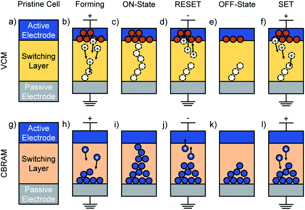 | ||
| Fig. 1 Illustration of the bipolar filament-type switching process in VCM (a–f) and CBRAM (g–l) cells. A pristine VCM cell (a), consists of an active electrode (typically Ti or Ta), an insulating switching layer made of a binary transition metal oxide such as HfOx, and a grounded passive electrode. Through the application of a forward external voltage, oxygen vacancies are formed at the active electrode–oxide interface (b). The resulting oxygen atoms are incorporated into an oxygen reservoir at the electrode, whereas the positively charged oxygen vacancies migrate under the electric field towards the passive electrode until they are reduced. A filament of neutral oxygen vacancies (c) assembles in the switching layer resulting in a drop of the resistance. This process is called the forming step. If a voltage of opposite polarity is applied, the oxygen vacancies are oxidized and migrate back towards the active electrode where they recombine with the available oxygen atoms (d). The resistance increases and the system returns to its OFF-state (e). Since parts of the filament remain in the switching layer, subsequent switching to the ON-state becomes faster than in the forming step. This is the SET process (f) and the cell switches to the state depicted in (c). A CBRAM cell is built of an active electrode (often Ag or Cu), an insulating switching layer (e.g. a-SiO2), and an inert metal electrode (g). The application of a forward voltage oxidizes the metal atoms at the interface of the active electrode. These ions migrate towards the passive electrode where they are reduced (h). Eventually, a stable metallic filament is formed that bridges the switching layer (i). By reversing the voltage polarity, the filament is disrupted (j), and the OFF-state with a partial filament left in the oxide layer is reached (k). The subsequent SET process (l) brings the CBRAM cell back to the ON-state (i). | ||
For HfOx- and SiOx-based VCM cells, an alternative model has been proposed in which oxygen vacancies are formed in the bulk rather than at the interface, creating anti-Frenkel defect pairs consisting of an oxygen interstitial and an oxygen vacancy.19–21 The oxygen vacancies are assumed to be immobile forming an oxygen-deficient filament. The interstitial oxygen ions, on the other hand, would be mobile and migrate under the applied electric field towards the active electrode forming an interfacial oxide layer. However, it was later shown that anti-Frenkel defect pairs are not stable in bulk hafnium oxide.17 Furthermore, it is energetically more favorable to form oxygen vacancies at HfOx interfaces rather than in the bulk.22
In addition to filamentary type switching, VCM is also proposed to operate in a volume-type mode where the total amount of oxygen vacancies stays constant.16 It relies on the redistribution of oxygen vacancies next to the active electrode during the switching process. If the oxygen vacancy concentration at the electrode–oxide interface is modified, the electrostatic barrier is altered according to the Schottky effect.23,24
The filament in CBRAM cells consists of metal atoms dissolved in the insulating layer. A broad range of materials have been reported as possible candidates for the insulating layer.6 Apart from chalcogenides, amorphous oxide films of SiO2, HfO2, ZrO2, or Al2O3 have attracted a lot of attention due to their compatibility with existing CMOS technologies. Typical materials for the electro-active electrode are Ag and Cu, whereas Au, Pt, or W are preferred for the electro-inactive side. In CBRAM, the application of an external potential triggers an oxidation of the metal atoms at the interface between the active electrode and the insulating layer.6 This oxidation generates metal cations, which migrate along the applied electric field towards the passive electrode where they are reduced. Eventually, a filament of neutral metal atoms forms and grows towards the active electrode.25 Once it bridges the oxide and connects the two electrodes, the electrical resistance drops by several orders of magnitude. The filament can be disrupted by applying a voltage of opposite polarity, leaving metallic ions that only partially span the switching layer. The remaining atoms can then be reused to create a new filament in subsequent SET processes.6,7
Although recent experimental studies26 shed light on the switching principle of RRAMs, the precise mechanisms that control the transition from the OFF- to the ON-state, as well as the nature of the conducting path, are still under intense investigation. Continuum models27 (Fig. 2(a)), in which partial differential equations describe the atomic motions (drift and diffusion), can very accurately reproduce and explain experimental data such as the I–V characteristics during a switching cycle28,29 or the conductive filament life time,30 at low computational cost. However, their efficiency depends on the availability of a large set of material parameters, that must be determined one way, e.g. from higher-order simulations, or another, e.g. through fitting. In addition, any information about the actual atomic configuration is lost, which might become an issue when the stochastic relocation of a few atoms can change the electronic current by several orders of magnitude.31 For instance, doping atoms reduce the formation energy of oxygen vacancies in VCM cells. The oxygen vacancies tend to then accumulate around the dopants, affecting the formation of the RRAM filament and impacting the overall device performance; both the electronic structure, which governs the conductivity of the switching layer, and the switching kinetics are strongly influenced.32 Therefore, atomistic models are needed to highlight the mechanisms underlying the switching behavior of RRAM cells.
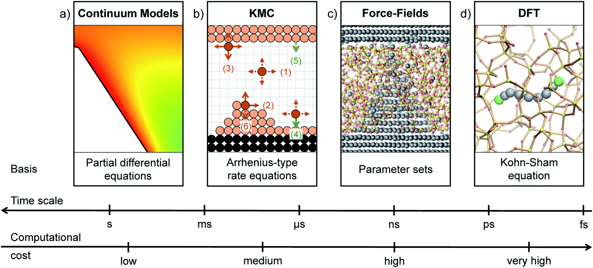 | ||
| Fig. 2 Overview of the modeling methods presented in Section 2.1 with CBRAM cells as an example. (a) Example of a 2-D continuum model providing an insight into the switching layer of a Ag/a-SiO2/Pt CBRAM cell. The white area represents the filament, the colored one the concentration of the Ag+ ions dissolved in amorphous SiO2 (a-SiO2). Continuum models do not offer atomic resolution, but are very versatile in terms of model size (typically ranging from μm to mm) and time scale. They are defined by (coupled) partial differential equations and are computationally inexpensive. (b) Schematic drawing of the working principle of a 2-D KMC simulation. In this model, the neutral atoms of the active material (bright orange), the positively charged metallic ions (dark orange), as well as the atoms of the passive electrode (black) are placed on a homogeneously spaced grid. In contrast, the oxide is not treated on an atomic level. The model relies on Arrhenius-type rate equations describing the various processes that occur in CBRAM cells, i.e. volume (1) and surface diffusion (2), desorption (3), adsorption (4), oxidation (5), and reduction (6). KMC models are capable of simulating full RRAM switching cycles at a moderate computational cost. (c) CBRAM cell with a cone-shaped filament consisting of Cu atoms embedded in a matrix of a-SiO2 created with FF-based MD. The interactions between the atoms are described by empirical parameter sets. Systems of up to a few hundreds of nm3, and MD trajectories of several tens of ns, can be simulated with this method. (d) Tracking of a single Cu+ ion migrating through a-SiO2 with DFT. The green spheres represent the initial and final state of the trajectory. Ab initio calculations offer a higher accuracy than FF-based methods, but are computationally very demanding. Therefore, the system size is limited to a few thousand atoms and AIMD trajectories can generally only be sampled up to a few ps. | ||
One such example is kinetic Monte Carlo33 (KMC) (Fig. 2(b)), a simulation approach that allows us to generate atomistic filament structures and to link them to continuum methods.34 The KMC simulation box is typically discretized into a grid with quadratic tiles representing the atomic positions. The edge length of a square (2-D) or cube (3-D) corresponds to the hopping distance of the filament forming species. In a KMC model, all relevant processes occurring in a RRAM cell, e.g. oxidation and reduction, adsorption and desorption, nucleation as well as ionic migration within the insulating layer or along interfaces, are described by rate equations obeying Arrhenius-type behavior.27 Each rate equation depends on the energy barrier that the specific reaction has to overcome, for instance the activation energy for ionic diffusion or the one for oxidation. Since the activation energy can be lowered by an applied voltage, the processes can be exponentially accelerated by increasing either the applied voltage or the temperature. The rate of each individual process is first calculated and stored in a table. At each step of the KMC algorithm, the event to be executed is randomly chosen based on the occurrence probability of the various processes. After each event, the atomic configuration is potentially modified until a stationary state is reached.
KMC has been successfully applied to grow and dissolve filaments with an atomic resolution in both CBRAM35,36 and VCM37 cells, with excellent agreement with experimental data. Despite valuable insights into the filament dynamics, structures generated with this method suffer from multiple limitations. First of all, most KMC models are two-dimensional, although three-dimensional implementations have been recently demonstrated.36,37 Second of all, cubic grids have difficulty treating amorphous structures, and materials with a non-cubic lattice are only approximately represented. Lastly, the switching layer, contrary to the filament, is described as a continuum, rather than at an atomic level. Thus, more advanced models are needed that can enhance the spatial resolution of KMC and better account for the broad range of material properties encountered in RRAMs.
Classical molecular dynamics (MD) based on force-field (FF) approaches (Fig. 2(c)) meet these requirements and can capture the detailed atomic structure of both the filament and the insulating layer as well as their dynamics. In such simulations, a parameter set describes the different types of atoms and their interactions. Dihedral angles, torsion, and chemical bonds are used to calculate the potential energy of a given system from which the forces acting on each atom can be derived. The parameters are fitted to reproduce reference data from experiments, quantum mechanical calculations, or both.38 The obtained forces are then used to determine the trajectories of the atoms based on Newton’s laws of motion. To model the growth and dissolution of a filament through the switching layer of an RRAM cell, simulation domains containing thousands of atoms must be constructed.39 Additionally, time spans of several nanoseconds must be considered to model a full switching cycle.10 FF-based molecular dynamics achieves that at reasonable computational cost.
Elaborate schemes are needed to construct suitable amorphous structures and interface them with metallic electrodes. For example, a melt-and-quench approach40 can be used for that purpose. Starting with a chunk of crystalline oxide or randomly placed atoms, MD is performed for several hundreds of picoseconds at a temperature above the melting temperature of the oxide. Then, the melt is quenched to 300 K with cooling rates in the order of −15 K ps−1.39 Post-quench annealing at room, or slightly elevated, temperature can be beneficial to eliminate coordination defects and reduce the stress inside the amorphous structure.
The first atomistic simulation of a complete CBRAM switching cycle was demonstrated by Onofrio et al.39 using a so-called reactive FF method. In contrast to traditional FFs, reactive force-fields such as ReaxFF41 are able to describe the formation and breaking of bonds and therefore to model chemical reactions. They rely on the charge equilibration formalism,42 which provides environment-dependent partial atomic charges. Onofrio et al.39 extended ReaxFF MD simulations with electrochemical dynamics including implicit degrees of freedom (EChemDID). This allows for the description of electrochemical reactions driven by the application of an external voltage. The effect of an electrochemical potential difference, ΔΦ, applied between two electrodes was modeled by altering the electronegativity, χ, of the atoms on the left and right electrode to χ + ΔΦ/2 and χ − ΔΦ/2, respectively.
A much simpler model of a conductive filament can be obtained by manually inserting metal atoms into the amorphous insulating layer instead of explicitly growing a structure. A shape must be defined and all atoms within it are replaced by metal. Subsequently, the obtained system is annealed using MD. It can be used as the starting point for reactive MD under an electric field. However, models relying on continuous, rather than localized, electric fields have not lead to realistic filament morphologies so far, at least not for complete ON–OFF switching cycles.43
A similar approach can be applied to VCM cells to create an oxygen vacancy filament in a layer of transition metal oxide. Starting from pristine amorphous oxide, oxygen atoms are removed by visual inspection resulting in a transition metal-rich region.44 Depending on whether the low- or high-resistance state should be modeled, a continuous or disrupted filament can be created.
The parameterization of force-fields is often tailored such that the processes of interest are accurately described, whereas less relevant phenomena are not well accounted for. Therefore, the usage of force-fields to perform MD in complex systems such as RRAM cells, where many different subprocesses are encountered, can result in misleading behavior. A higher level of accuracy can be achieved using ab initio molecular dynamics (AIMD) where the forces acting on each atom are derived from DFT. The latter is a quantum mechanical modeling method that can describe the electronic structure of any given atomic configuration without the need for fitting parameters (Fig. 2(d)). However, the high computational demand limits the time range accessible by AIMD to a few picoseconds and the system size to a few thousand atoms.45
To benefit from the advantages of FFs and DFT, both methods can be combined.40 First, atomistic filamentary type RRAM structures are created using FF approaches as outlined above. Then, the structures are relaxed and optimized using AIMD before a variety of physical properties such as the evolution of the electronic density of states (DOS),45 the activation energy of ion diffusion46 as well as the nucleus formation energy47 in CBRAM cells, or the formation energy of oxygen vacancies in VCM cells32 are extracted with the help of DFT. Due to the disordered nature of the structures, calculating meaningful physical properties can only be achieved by averaging over an ensemble of independent measurements.45 For each of them, the corresponding Hamiltonian can be used in quantum transport simulations to compute electrical and thermal currents as well as self-heating effects, which is the topic of the next section.
2.2 Ab initio quantum transport (DFT + NEGF)
Density functional theory is a computational method to evaluate the ground-state electronic structure of many-body systems, where atoms and electrons interact with each other. Its foundations were developed in the seminal works by Hohenberg et al.48 and Kohn et al.,11 which provide a framework to replace the interacting electrons by a computationally more favorable auxiliary system of non-interacting particles. The interactions, namely exchange and correlation, are incorporated into an exchange–correlation potential. As no exact form of this potential could be established up to the present, a wide range of approximations have been proposed, with greatly varying accuracy and computational burden.49The NEGF formalism offers a powerful framework to calculate the non-equilibrium properties of quantum mechanical systems.50 It is widely used to perform quantum transport (QT) simulations.51,52 This approach to non-equilibrium statistical mechanics is based on the work of Kadanoff and Baym,12 and Keldysh.53 It requires a description of the electronic structure of the system under study in the form of a Hamiltonian matrix. A number of strategies have been proposed and tested to construct this quantity. Notable examples are the tight-binding (TB)54 and effective mass approximation (EMA),55 as well as approaches relying on first-principles concepts, where the Hamiltonian matrix is obtained from DFT calculations.13,14,56 Such a coupling of NEGF and DFT to perform ab initio QT calculations was introduced by Lang,56 where the representation of the device was based on DFT and the electrodes modeled using a jellium approximation. Fully atomistic simulations were proposed by Taylor et al.13 featuring an atomistic representation based on DFT for both the device region and the contacts. Since these pioneering examples, several packages capable of treating quantum transport from first-principles have been developed.57–62 Some of them are freely available, others commercially available.
The majority of DFT + NEGF calculations are performed in the ballistic limit of transport, where the energy of each particle is conserved throughout the simulation domain. The effect of inelastic interactions can naturally be incorporated in NEGF through the use of scattering self-energies.63 Besides pure electrical or thermal transport, coupled electro-thermal simulations can be perturbatively carried out through the self-consistent Born-approximation (SCBA).15,64 Owing to the large computational burden induced by the SCBA, such simulations are typically restricted to small systems or require large computational resources. Furthermore, calculating the phonon properties and the electron–phonon coupling from first-principles is a challenging task.65,66 Nevertheless, such calculations have been applied to a wide range of nanoscale devices going from 2-D field-effect transistors (FETs),65 FinFETs,66 or CBRAM cells31 to the modeling of inelastic electron-tunneling spectroscopy (IETS) in molecular junctions.67,68
It should be noted that the SCBA is not the only possibility to account for electro-thermal effects. Lowest order-expansion techniques have been used as well. They have a lower computational burden, but at the cost of additional approximations.67,69 Due to its perturbative nature, SCBA may fail to converge in the presence of strong electron–phonon coupling. An exact, but also computationally more expensive, technique capable of treating such systems is the hierarchical equations of motion.70
The DFT + NEGF framework is not limited to steady-state simulations. It is capable of delivering insight into time- and frequency-resolved quantum transport phenomena as well.71 Due to the heavy computational burden of these simulations they have only recently seen a rise in popularity. While NEGF is frequently used for electrical and thermal QT simulations the formalism can be applied to any quasi-particle that follows the laws of quantum mechanics. It has, among others, also been employed to study the adsorption on metal substrates72 and solid-plasma surfaces.73
The remainder of this paper is dedicated to the description of ab initio electro-thermal QT calculations within the SCBA. The following sections describe the coupling of DFT with NEGF for the case of electrical and thermal transport. Subsequently, the coupling of electrons and phonons via scattering self-energies is explained.
2.3 Ballistic transport
| ĤKS|Ψ〉 = E|Ψ〉 | (1) |
 | (2) |
It contains two terms, first the kinetic operator −∇2/2 and then the effective potential
 | (3) |
The three terms above correspond to the Hartree, the exchange–correlation, and the external potential with ρ(r) denoting the charge density at position r. The Hartree potential includes the electron–electron Coulomb repulsions. The second term in eqn (3), VXC, accounts for all electron many-body effects, namely electron exchanges and correlations, whereas the influence of external voltage sources are cast into the last one, Vext. DFT takes advantage of the Born–Oppenheimer approximation, which enables a separate treatment of the valence electrons and atomic cores. Electrons freely move in the potential induced by these static cores, which are also described by the external potential.
Multiplying eqn (1) with 〈Ψ| gives rise to the Hamiltonian and overlap matrices
| H = 〈Ψ|ĤKS|Ψ) and S = 〈Ψ|Ψ〉 | (4) |
| H·ψ(E) = ES·ψ(E), | (5) |
The computational efficiency of solving matrix equations can be directly related to the number of non-zero elements and the sparsity pattern. To maximize the sparsity of H and S a suitable basis must be selected to expand |Ψ〉. Localized basis sets such as Gaussian-type orbitals (GTO)75 are ideal for that as they produce sparsely populated, banded matrices. In contrast, plane-waves, which are popular for electronic structure calculations, lead to dense matrices. While not impossible,76,77 the use of plane-waves is relatively scarce in quantum transport calculations, in particular for large systems. If necessary, plane-waves can still be localized, with the help of e.g. Wannier functions.78 When employing a localized basis set, |Ψ〉 becomes
 | (6) |
The valence electrons of atom n are expanded in l(n) basis functions ϕln centered at position rn. The number of basis functions per atom l may vary for different chemical species. The cln(E) are the occupation coefficients of the respective basis function. The wave function is then the sum over all individual basis functions of each atom weighted by the occupation factor. With this choice of basis expansion ψ(E) becomes a vector containing all coefficients cln(E), and the size of the matrices H and S is the sum of l(n) over all atoms. If the ϕln are orthogonal to each other, S is the identity matrix and eqn (5) becomes a regular eigenvalue problem (EVP). In most cases the overlap between localized basis functions is non-zero and a generalized EVP must be solved.
It should be noted that the H and S matrices are not unique to DFT. They can also be created based on other methods such as tight-binding (TB),54 where Löwdin orbitals are parameterized to reproduce experimentally measured, or DFT, band structures. The Hamiltonian is not necessarily an atomistic quantity either, it could be expressed in the effective mass approximation (EMA) on a discretized grid.55 The transport equations presented in the next paragraphs apply to Hamiltonian matrices obtained with these methods as well. The continuum nature of EMA and the required TB parameterization, however, make both methods ill-suited to deal with disordered structures. The major difficulty in TB models lies in the derivation of a parameter set that accurately captures amorphous phases or defects such as vacancies and interstitials.
In contrast to electronic structure calculations, which are typically restricted to the ground state of a system, electrons in device simulations must be able to enter and leave an open domain so that a non-equilibrium current can flow. External potentials are applied to contact regions to drive a device out of equilibrium. As a consequence, the boundary conditions applied to eqn (5) require special attention. Whereas periodic (PBCs) or closed boundary conditions (CBCs) are typically used in DFT, open boundary conditions (OBCs)79 are at the core of quantum transport investigations. In OBCs the contacts and the device region are first treated separately, as illustrated in Fig. 3(a). Each contact is modeled as a semi-infinite lead in thermal equilibrium, with a flat electrostatic potential, as shown schematically in Fig. 3(b). It should be represented by at least two identical blocks of atoms. These blocks correspond to the first and last unit cell of the central (device) region. The leads serve as launching pads for electrons or as collectors. They are connected to the device through so-called retarded boundary self-energies ΣR,B(E) that must be introduced into eqn (5). Additionally, an injection vector Inj(E) acts as a source term to model the incoming electrons. OBCs are not limited to two-terminal systems, but can be readily generalized to structures with multiple leads.79
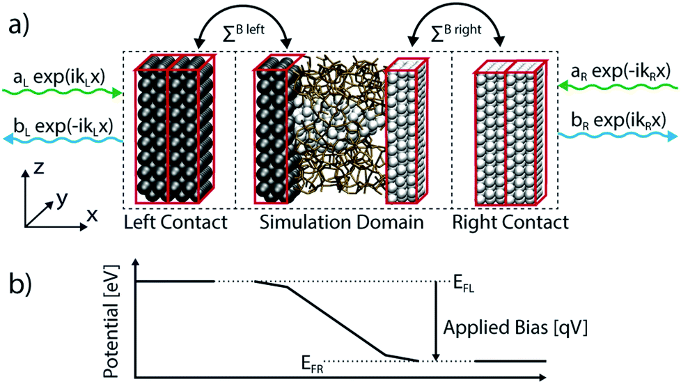 | ||
| Fig. 3 (a) Illustration of the RRAM atomic simulation domain and its division in three regions. The open boundary conditions are calculated in the leads based on a plane-wave ansatz. Incoming (green) and outgoing (blue) waves are considered. The incoming waves inject electrons into the simulation domain with a probability aL (from the left) and aR (from the right). The outgoing waves encompass the transmitted and reflected electrons with amplitudes bR and bL, respectively. The leads are coupled to the simulation domain through the boundary self-energies, ΣB. (b) Average electrostatic potential of a typical RRAM along the x-axis. The potential in the leads is constant so that plane-waves are the exact solution of the Schrödinger equation in these regions. The potential difference between the left (EFL) and right (EFR) Fermi energy is proportional to the externally applied voltage. | ||
In the presence of OBCs eqn (5) takes the following form
| (ES − H − ΣR,B(E))·ψ(E) = Inj(E). | (7) |
This equation must be solved for all discrete energies belonging to the interval of interest, which extends over the Fermi energy of both contacts. In ballistic and coherent simulations, i.e. in the absence of scattering with energy relaxation, all E’s are independent of each other and eqn (7) directly yields ψ(E). Such an approach is known as the quantum transmitting boundary method (QTBM).80 It is computationally attractive as it involves the solution of sparse linear systems of equations with multiple right-handed-sides, but it does not lend itself naturally to the simulation of dissipative transport.
Alternatively, eqn (7) can be rewritten in terms of Green’s functions (GFs) as
| (ES − H − ΣR,B(E))·GR(E) = I, | (8) |
| G≶(E) = GR(E)·Σ≶,B(E)·GA(E), | (9) |
| ψ(E) = GR(E)·Inj(E). | (10) |
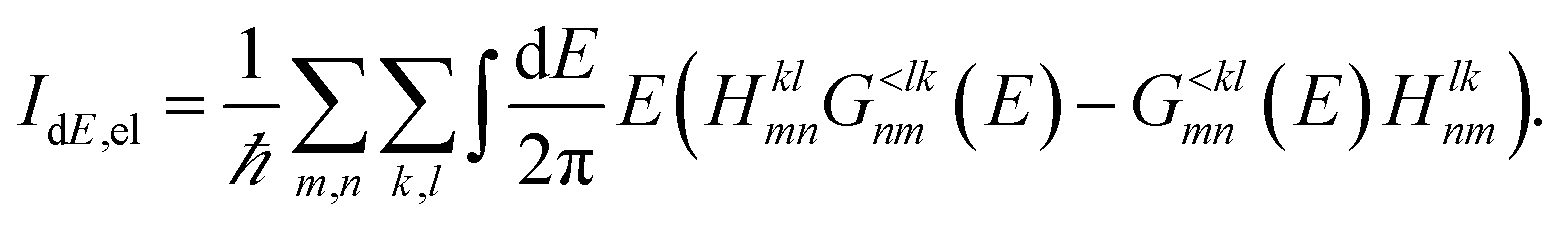
Eqn (8) and (9) are known as the non-equilibrium Green’s function (NEGF) formalism.12 Intuitively, the lesser (greater) boundary self-energy, ΣB,≶(E), indicates the probability that a state gets filled (ΣB,<(E)) or emptied (ΣB,>(E)) through interactions with the contact. The off-diagonal elements of the lesser and greater GF, G≶(E), describe the correlation between the involved basis functions, whereas the diagonal entries contain the probability that a state n is occupied (G<nn(E)) or unoccupied (G>nn(E)). Therefore, it is not necessary to convert back the results of eqn (8) and (9) to a wave function ψ(E). All observable quantities such as the charge density ρ(r) at position r and the electrical current Id can be directly derived from selected entries of G≶(E). The latter can be computed efficiently with an iterative algorithm called the recursive GFs (RGF) algorithm.81 Nevertheless, for ballistic simulations this approach is computationally more expensive than QTBM. The strength of NEGF comes from its natural integration of scattering mechanisms through self-energies, as will be introduced in Section 2.4.
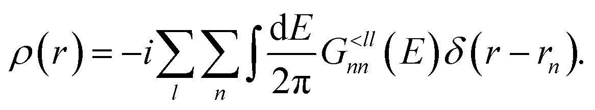
Regardless of the transport type, the charge density ρ(r) can be computed as
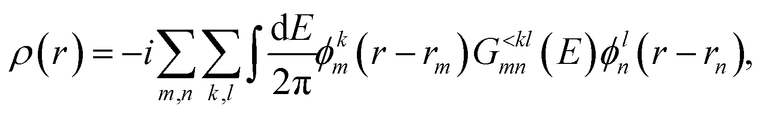 | (11) |
 | (12) |
Injecting electrons into the device domain drives it out of equilibrium, which changes the distribution of electrons and modifies the charge density ρ(r). This in turn affects the Hamiltonian H through the first two terms in the effective potential Veff(r) in eqn (3), giving rise to a mutual dependence of eqn (2), (8) and (9). It must be resolved in a self-consistent manner until ρ(r) is converged.13
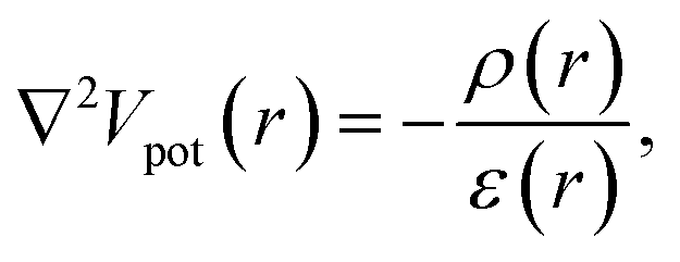
Fully coupled NEGF + DFT simulations come with a heavy computational burden, even in the ballistic case. This can be somewhat alleviated by assuming that the charge density only affects the electron–electron repulsions and by neglecting the change of exchange and correlation. By solving Poisson’s equation
 | (13) |
 | (14) |
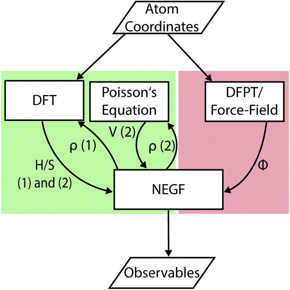 | ||
| Fig. 4 Flow chart illustrating the interactions between the different methods used to perform DFT + NEGF simulations. The data flow for the section covering electrons is shown in green, the one for thermal transport in red. Electron transport does not require any input beside the coordinates of the atoms. For a given atomic system relaxed with DFT the Hamiltonian H and overlap S matrices are passed to NEGF. Subsequently, either the NEGF-DFT (1) or the NEGF-Poisson (2) loop is executed until the charge density ρ is converged. Lastly, observables such as the electrical and energy currents are computed. The path for thermal transport has no feedback loop because the dynamical matrix Φ is assumed not to depend on any out-of-equilibrium quantity. In addition to the atomic coordinates a parameterization of the forces is needed in classical approaches to obtain the dynamical matrix. This requirement is superfluous if the dynamical matrix is calculated at the ab initio level. | ||
After convergence of the selected self-consistent loop, physical observables can be extracted. In ballistic simulations the function T(E) describes the transmission probability of an electron from the left to the right side of an open system (or vice versa) at energy E.63 It is calculated according to
T(E) = ΓL(E)GA(E)![[thin space (1/6-em)]](https://www.rsc.org/images/entities/char_2009.gif) ΓR(E)GR(E). ΓR(E)GR(E). | (15) |
The broadening function ΓC(E) of contact C depends on the boundary self-energy ΣBC(E) and is defined as
| ΓC(E) = i(ΣB,RC(E) − ΣB,R†C(E)), with C = R or L. | (16) |
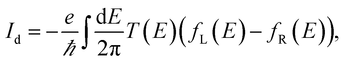 | (17) |
 | (18) |
 | (19) |
This formulation of the electrical and energy currents, Id and IdE,el is more general and holds even when no transmission function can be defined, i.e. in the presence of a dissipative scattering mechanism.
Phonons are quasi-particles that arise from the coupled motion of atoms around their equilibrium position.55 An illustration of such a wave of coupled atomic motions is given in Fig. 5(a) for a 1-D wire. What is represented is an excited state of the lattice whose amplitude is related to the crystal temperature. To mathematically describe phonons, the total energy, Etot, of a perturbed atomic system with equilibrium energy E0 should be considered. The displacement of atom m along the cartesian direction i is labeled dim. In the harmonic approximation, Etot is expanded in a Taylor series up to the second order of the displacement
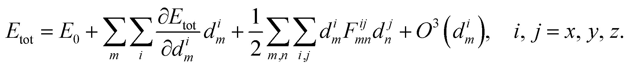 | (20) |
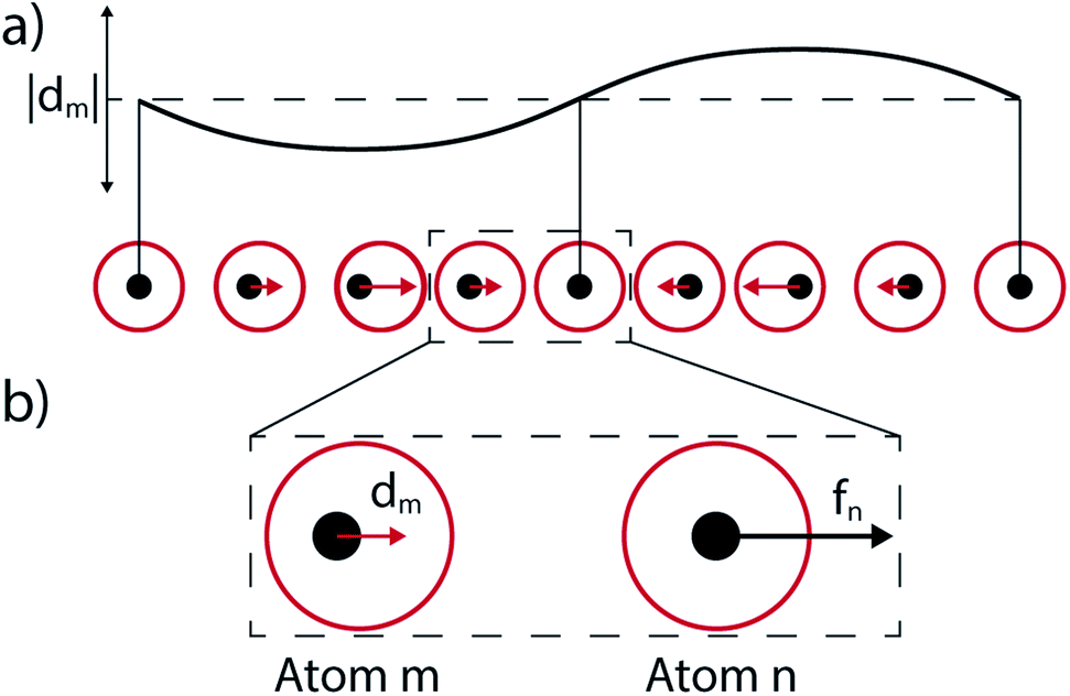 | ||
| Fig. 5 (a) Visualization of a phonon wave. The black dots represent a 1-D chain of atoms in their equilibrium position. The larger red circles around the atoms help visualize their current displacement, which is marked by the horizontal arrow. The first, middle, and last atom remain at their equilibrium position. The curve above the atoms illustrates the envelope of the phonon wave function. The magnitude of the atomic displacement is proportional to it. (b) Illustration of the interplay between the displacement of an atom and the force it induces on a neighbor atom. Atom m is moved by the vector dm towards atom n. Consequently, the latter feels a repulsive force fn even though it remains at its lattice site. | ||
In an equilibrium configuration the system resides in a (local) minimum so that dEtot/dim, the force acting on atom m in direction i, vanishes from eqn (20). The second-order term
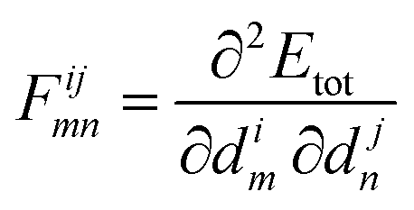 | (21) |
| Φ·μ(ω) = ω2μ(ω). | (22) |
 , Mm/n being the mass of atom m/n, and μ(ω) the phonon wave function or polarization vector. The energy of a phonon is related to its frequency through E = ℏω. As Hamiltonian matrices may be k-dependent quantities, Φ may depend on the phonon wave vector q. Here, this dependence is neglected for the same reasons given for electrons and only the Γ-point is considered.
Eqn (22) is the phonons equivalent of eqn (5) for electrons. To derive the thermal NEGF equations, OBC are introduced into eqn (22). They can be constructed following the same prescriptions as for electrons illustrated in Fig. 3(a). Their calculation takes either the form of an eigenvalue problem86 or of a complex contour integral.87 By incorporating the resulting phonon boundary self-energies ΠB into eqn (22) and by transforming the wave function expressions into GFs, we obtain the following system of equations to solve:
| (ω2I − Φ − ΠR,B(ω))·DR(ω) = I | (23) |
| D≶(ω) = DR(ω)·Π≶,B(ω)·DA(ω). | (24) |
The quantities in the equations above are the phonon GFs (DR, DA and D≶) and the boundary self-energies (ΠR,B and Π≶,B). The labeling conventions for retarded, advanced, lesser, and advanced remain the same as in the previous section. Eqn (23) and (24) must be solved for all phonon frequencies of interest. The phonon density and current are then derived from D< using similar expressions as for the electrons. Besides, the energy current carried by phonons can be computed as
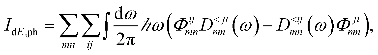 | (25) |
While eqn (23) and (24) have the same form as the equations for electrons, there is an important difference. Namely, eqn (22) does not depend on the phonon population, therefore eliminating the need for an iterative solution process and reducing the computational cost as compared to electrons. The procedure involved in atomistic thermal transport simulations is depicted in the right-hand side of Fig. 4.
Whereas DFT has become the most widely used method for electronic structure calculations, even in large systems, competing approaches exist to generate the dynamical matrix Φ in eqn (22).89 It can be directly produced from the total energy of a given system with density functional perturbation theory (DFPT).90 Alternatively, it can be observed that Fijmn in eqn (21) corresponds to the first derivative of the forces acting on each atom. It can therefore be calculated from finite differences through the frozen phonon scheme.85 Both DFPT and frozen phonons induce a large computational burden that make them impractical for large atomic systems, if performed at the ab initio level.
The frozen phonon approach is the method of choice for large, disordered systems because of its relatively low computational complexity. It relies on the evaluation of the first derivative of the force fim = dEtot/drim using forward or central differences67,85
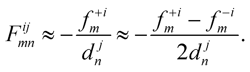 | (26) |
2.4 Electro-thermal coupling
Ballistic electron and phonon transport simulations, as introduced in the two previous subsections, provide valuable insight into a large variety of device operation regimes. To offer a comprehensive picture under any bias condition and to investigate certain failure mechanisms such as temperature-induced breakdowns, coupled electrical and thermal simulations are required. The electron–phonon (e–ph) interactions can take different forms, e.g. electron scattering on deformation potentials91 or scattering on polar-optical phonons through the Fröhlich interaction.92 The computational framework to couple electron and phonon transport is the same in all cases, the difference coming from the electron–phonon coupling elements. Subsequently, a description of scattering on deformation potentials is given.To couple the electron and phonon populations, the energy of the fermionic and bosonic system must be considered. It can be described by the total Hamiltonian
| Htot = H + Hph-kinetic + Hph-harmonic + He–ph. | (27) |
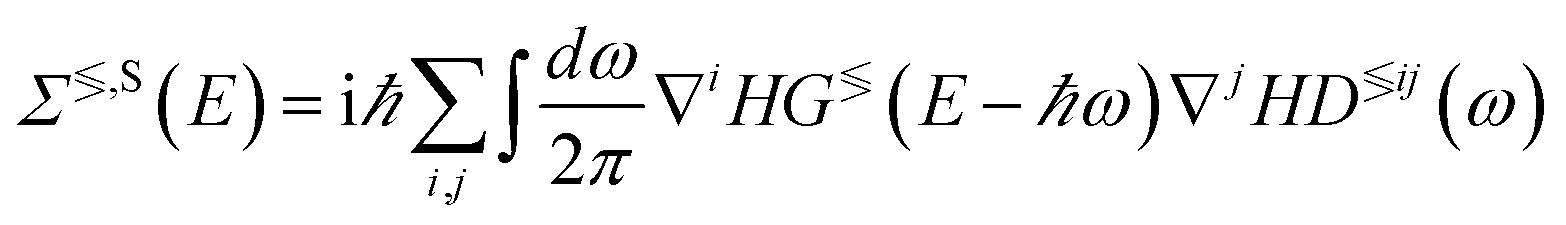
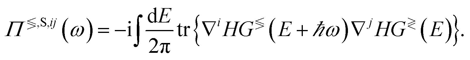
The first term corresponds to the electron Hamiltonian from eqn (5), while the second and third ones are captured by the dynamical matrix Φ. The last Hamiltonian contains the interaction between electrons and phonons. It is treated perturbatively and cast into the scattering self-energies ΣTS and ΠTS of type T ∈{R, A, <, >} for electrons and phonons, respectively. The lesser and greater components can be written as84
 | (28) |
 | (29) |
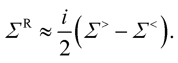
In eqn (28) and (29), all G≶, Σ≶, and ∇H blocks are matrices of size Norb × Norb with the summation over neighbor atoms omitted for brevity. The superscripts i and j denote the entries in ∇H, the phonon GFs, and self-energies corresponding to the cartesian coordinates i and j ∈{x, y, z}. The strength of the electron–phonon coupling is determined by ∇iH, which represents the derivative of the electron Hamiltonian with respect to the displacement of the atoms along the direction i. It thus couples the lattice dynamics created by the phonons to its electronic response. The retarded scattering self-energies ΣR,S and ΠR,S can be derived from Σ≶,S and Π≶,S. Very often, their real part is neglected for simplicity.63
To give an intuitive interpretation of eqn (28) and (29), we first recall that the diagonal elements of the lesser GFs, G<(E) and D<(ω), indicate whether a state at energy E is occupied by an electron and the number of phonons that occupy a state at energy ℏω. The same elements of the greater GFs, G>(E) and D>(ω), determine whether a state is unoccupied or the number of free states at the energy E and ℏω. A specific transition is only possible if an (un-)occupied electron state is available at an energy ℏω above or below the state of interest, as illustrated in Fig. 6(a). If a scattering event is allowed, the likelihood of in-scattering, i.e. an empty state at energy E, G>(E), gets filled is proportional to the lesser scattering self-energy Σ<(E). Such a process can happen through either phonon emission or absorption. An electron at energy E ± ℏω (G<(E ± ℏω)) emits (+) or absorbs (−) a phonon with energy ℏω (D>(ω) for emission, D<(ω) for absorption) and changes its energy to E. The out-scattering probability is given by Σ>(E). An occupied state at energy E, G<(E), gets emptied to E ∓ ℏω (G>(E ∓ ℏω)) by emission (−) or absorption (+) of a phonon (D>(ω) and D<(ω)). A similar interpretation can be made for the phonon scattering self-energies Π≶(ω). They refer to the probabilities that an unoccupied (D>(ω)) or free (D<(ω)) state gets filled (Π<(ω)) or emptied (Π>(ω)) when an electron transitions from one state to the other through phonon emission or absorption.
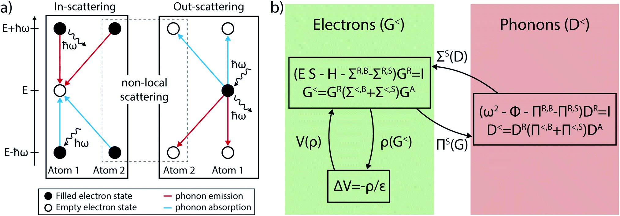 | ||
| Fig. 6 (a) Scattering events leading to a change in the energy of an electron when they interact with phonons. These events can be divided into two categories: in- and out-scattering. In the in-scattering case an empty state at energy E is filled by an electron at energy E ± ℏω by emission or absorption of a phonon with energy ℏω. Out-scattering describes the situation where an occupied state is emptied to a state at E ∓ ℏω by emitting or absorbing a phonon with energy ℏω. Both in- and out-scattering can be local or non-local events. In the former case the involved electron remains located on the same atom, whereas in the latter it may relocate to a different place. (b) Coupled electron–phonon system of equations within NEGF. The coupling is included perturbatively through the scattering self-energies ΣS and ΠS, that must be solved self-consistently with the GFs. This process is known as the self-consistent Born approximation (SCBA). | ||
The diagonal entries of the scattering self-energies describe local interactions, that is, the electron remains on the same atom during the process. The off-diagonal elements, on the other hand, account for non-local transitions where the electron does not only change its energy, but also its position in real space. Non-local scattering events are numerically difficult to handle. In our approach they are neglected for electrons and only close-neighbor interactions are taken into account for phonons. This is necessary to ensure energy conservation in our NEGF calculations. By scaling the strength of the local entries of Σ≶, the influence of the non-local events can be indirectly modeled.93
The derivative of the Hamiltonian matrix from eqn (4) with respect to a perturbation in real space, ∂r, is given by
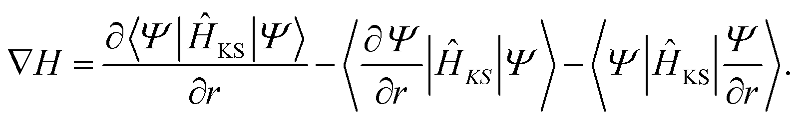 | (30) |
The last two terms appear because the basis changes with perturbation.67 The expression in eqn (30) can be computed at various levels of accuracy. The simplest picture considers the derivative of the Hamiltonian with respect to bond stretching between two neighboring atoms.94 This scheme can be expanded to include more harmonic terms, e.g. bond angles. An alternative approach, similar to the calculation of the dynamical matrix, helps to determine ∇H with respect to the displacement of each individual atom. This is the most accurate method as it does not rely on any assumption regarding the nature of the bonds or angles connecting two atoms, but it comes at the price of increased computational cost. While the bond stretching technique only requires us to perform one additional ground-state DFT calculation under hydrostatic strain, typically 0.01% to 0.1%, the second method is even more expensive than computing the dynamical matrix from first-principles. Because of this, the bond stretching approach is the preferred one for large systems.
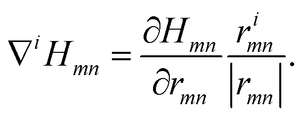
The chosen hydrostatic stress is applied to the atomic configuration by increasing the simulation box, thus stretching the bond rmn between atoms m and n without affecting the angle between them. If the change in basis functions induced by the stress is small, the last two terms in eqn (30) vanish. The strained Hamiltonian Hs is then computed and the derivative, with respect to a change in the bond length, evaluated as
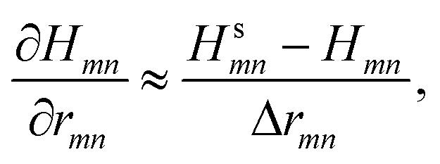 | (31) |
 | (32) |
When the scattering self-energies are included in NEGF the equations for electrons become84
| (ES − H − [ΣR,B + ΣR,S])·GR = I | (33) |
| G≶ = GR·[Σ≶,B + Σ≶,S(G≶,D≶)]·GA, | (34) |
 | (35) |
For phonons we have
| (ω2I − Φ − [ΠR,B + ΠR,S])·DR = I | (36) |
| D≶ = DR(ω)·[Π≶,B + Π≶,S(G≶,G≷)]·DA, | (37) |
 | (38) |
The dependence of the GFs and self-energies on the energy E and frequency ω has been left out in the above equations and substituted by D≶ and G≶ for the scattering self-energies, to emphasize the interplay between the electron and phonon populations. Eqn (33) and (34) now depend on eqn (36) and (37) and vice versa. These two sets of equations must be solved iteratively until convergence is reached. The fulfillment of this property can be verified by looking at the electrical current, eqn (18), and the sum of the electronic and thermal energy currents, eqn (19) and (25). Both quantities have to be conserved along the transport axis of the investigated device, when the GFs do not vary anymore. This process is known as the self-consistent Born-approximation (SCBA). The system of equations to be tackled is depicted in Fig. 6(b).
After converging the electron and phonon densities, physical quantities can be extracted. In addition to the currents that are given by eqn (18) and (25), the lattice temperature is of particular interest to quantify the effect of self-heating. Different possibilities exist to assign a local temperature to individual atoms.84 In the so-called population approach the effective temperature Teffn of atom n is adjusted such that the Bose–Einstein distribution reproduces the phonon population of each individual atom, Neffn. The phonon density is derived from the GF
 | (39) |
 | (40) |
3 Applications
Three device studies have been selected to illustrate the quantum transport simulation approaches presented in the previous section and to demonstrate their capabilities: (1) the ON-state properties and electro-thermal effects of a single Cu/a-SiO2/Cu CBRAM cell,31 (2) the dependence of these properties on the thickness of the oxide layer,10 and (3) the impact of the metal contact on the device current in a given filament configuration will be investigated.95 These three examples show how ab initio device simulations can reveal the physics behind the operation of atomic-scale components, thus accelerating and improving their design. The procedure to obtain the atomic structures and perform QT simulations is summarized here.The considered atomic CBRAM structures are assembled with the melt-and-quench approach detailed in Section 2.1, and depicted in Fig. 7(a)–(c). The switching layer is made of amorphous SiO2 (a-SiO2) with a density of 2.20 g cm−3. Melting happens at 3000 K for 600 ps. It is followed by a cooling phase with a rate of −30 K ps−1 to reach 300 K. The MD simulations are performed with a ReaxFF force-field,39 as implemented in the QuantumATK 2017.1.62,96 Next, metal electrodes, Cu or Ag, are attached to the a-SiO2 layer and a conical filament is inserted by replacing the Si and O atoms with Cu or Ag ones. The obtained configurations are annealed with AIMD at 800 K for 3–4 ps to relax the stress induced by the insertion of the metallic filament.
 | ||
| Fig. 7 (a) The melt-and-quench procedure to generate samples of a-SiO2. A box with crystalline SiO2 or randomly placed Si and O atoms is melted at 3000 K. Subsequently, it is cooled at a rate of −30 K ps−1 and annealed at 300 K. The melt-and-quench is performed classically, the post-annealing and optimization with DFT. (b) The metal–insulator–metal structure of a pristine CBRAM cell. Metal electrodes are attached to a slab of a-SiO2 obtained with the procedure from (a). (c) Filamentary configuration of a CBRAM cell in the ON-state. A metal filament is inserted into the a-SiO2 from (b) by replacing all Si and O atoms within a cone and annealing the result with DFT. (d) Energy-resolved transmission function around the Fermi energy for the structure shown in (c) using two basis sets, DZVP (solid blue line) and SZV + 3SP (dashed red line). Subplots (b)–(d) are adapted from ref. 31. | ||
The DFT simulations are executed with the CP2K package.97 This tool employs a Gaussian-type orbital (GTO) basis set with the linear combinations of atomic orbitals (LCAO)74 method. Such a localized basis is suitable for subsequent NEGF quantum transport simulations. All metal atoms are represented by a double zeta-valence polarized (DZVP)98 basis set to construct the atomic structure, while a single zeta-valence (SZV) basis is used to calculate the H and S matrices required for eqn (5). The larger DZVP basis set is required to produce meaningful device geometries, but the small SZV set is accurate enough for transport simulations31 as illustrated in Fig. 7(d). The 3SP parameterization of Zijlstra et al.99 is employed for the Si and O atoms, both in MD and quantum transport. In conjunction with the GTO basis set the atomic cores and inner electrons are described by the pseudopotentials of Goedecker–Teter–Hutter (GTH).100 The exchange–correlation energy is approximated by the PBE functional.101 No k-point grid is used; all calculations are performed at the Γ-point only. After obtaining the final atomic structure, the Hamiltonian and overlap matrices in eqn (5) are created in CP2K. The electron–phonon coupling elements are computed with the proposed bond stretching scheme introduced in Section 2.4 and rely on hydrostatically strained Hamiltonians. This approach is computationally less intense than more elaborate ones, especially for large systems.
The dynamical matrix accounting for the thermal properties is determined with the frozen-phonon approach discussed in Section 2.3.2. Computing the forces required to construct Φ from first-principles is prohibitive for our systems that comprise more than 3000 atoms. Therefore, these calculations were performed using a ReaxFF41 force-field specifically parameterized39 to model the switching behavior of CBRAM cells.
The Hamiltonian, overlap, and dynamical matrices, as well as the derivatives of the Hamiltonian, are imported into the OMEN quantum transport simulator.86,88 The latter implements the NEGF-Poisson scheme for electrons, phonons, and their coupling as detailed in Sections 2.3 and 2.4. The NEGF simulations for electrons are performed in the low field limit, which assumes that the applied bias does not significantly alter the electron density within the considered domain. Thus, the Hamiltonian and overlap matrices from CP2K are not updated based on the non-equilibrium charge and Poisson’s equation is not solved, thereby considerably reducing the computational burden.
3.1 Filament in a Cu/a-SiO2/Cu cell
Here, we examine the electro-thermal effects in a single metallic filament based on ref. 31. The atomic structure of this device is displayed in Fig. 7(c). It is composed of a slab of a-SiO2 sandwiched between two Cu electrodes. A thin conical Cu-filament is embedded within the SiO2 and connects the two contacts. The entire cell contains 4449 atoms, 3456 of which are Cu, the rest are Si (331) and O (662). The length of each electrode is set to 4.1 nm along the transport direction x, the insulator to 3.5 nm, and the cross-section in the yz-plane measures 2.1 × 2.2 nm2. In the case of ballistic transport only the NEGF equations for electrons, eqn (8) and (9), are solved. In the electro-thermal calculations, the coupled NEGF equations are solved for both electrons and phonons until the electrical and energy currents are converged within 1%.The current flowing through the filament configuration of Fig. 8(a) was computed both in the ballistic limit and under the influence of electron–phonon interactions. The resulting I–V characteristics are shown in Fig. 8(b). Ohmic behavior is revealed at low biases, i.e. a linear increase of the current vs. voltage. The electron–phonon limited current reaches about 69% of the value of the ballistic one at room temperature. The impact of scattering on the magnitude of the electrical current is rather low, which is to be expected from such a short device. The resistance, extracted as a linear fit to the I–V curve, is 48.1 kΩ in the ballistic case and 57.6 kΩ in the dissipative one. These values lie in the range of typical CBRAM ON-state resistances.6 The current field lines corresponding to an applied voltage of 0.2 V are rendered in Fig. 8(a). They confirm that the current follows the metallic filament and exhibits its largest density at the tip, i.e. at the thinnest part of the filament. The influence of electron–phonon scattering on the current can be best visualized in the form of a spectral plot representing the energy- and spatial location of the current given in Fig. 8(c). Electrons lose part of their energy when propagating through the device. Such energy dissipation is not possible in ballistic electron transport. Most of the energy loss occurs close to the tip of the filament or in the metallic contact attached to it. This fact agrees well with the observation that the device operates close to its ballistic limit. The electrons cross the oxide layer too fast to relax their energy therein. It should also be noted that a large portion of the electron population enters (leaves) the simulation domain with an energy below (above) the Fermi energy of the respective contact. This indicates that a lot of the power dissipation happens outside the simulated device, namely in the leads. The fraction of power that is consumed within the simulation domain is called the internal dissipation fraction and is labeled α. It can be computed as
 | (41) |
 | ||
| Fig. 8 (a) Atomic structure of a CBRAM cell containing a metallic filament. The copper atoms are represented by the gray spheres, silicon and oxygen by the orange ones. The current flowing through this configuration upon an external bias of 0.2 V is plotted with blue-red lines. The red color at the tip of the filament (right-hand-side of the oxide layer) indicates a large current density which decreases (dark blue) towards the left. (b) Ballistic (blue triangles) and electron–phonon limited (red diamonds) I–V characteristics of the device in (a). A linear fit to the data points is given with the blue dotted (ballistic) and red dashed (e–ph) lines. (c) Energy- and position-resolved current flowing through the cell in (a) in the presence of electron–phonon scattering. The largest current density is observed just below (above) the equilibrium potential in the left (right) contact, which is indicated by a white line. (d) Atomically-resolved temperature in the device in sub-plot (a) at an applied bias V = 0.2 V. The heating is more prominent in the copper atoms in the right half of the filament, marked by the red color. (e) Atomic temperature projected onto the x-axis (transport). The filament atoms are marked with the red diamonds, the oxide by the red dots. The vertical dashed lines indicate the electrode-device transitions. The black line refers to the average temperature over the cell cross-section (yz-plane). The maximum temperature is taken as the top of this black curve. (f) Maximum temperature and dissipated power as a function of the CBRAM device current. The simulated values are given as symbols. A quadratic fit of the data is superimposed as dashed (power dissipation) and dotted (maximum temperature) lines. Subplots (a)–(f) are adapted from ref. 31. | ||
Due to energy conservation, a reduction in electron energy must be compensated for by the creation of additional phonons corresponding to an increase of the lattice temperature. Generally, the temperature is an average quantity characterizing an ensemble of particles embedded within a reservoir. It is therefore a macroscopic property. Nevertheless, by relating the excess phonon population on each atom to an equilibrium temperature through the Bose–Einstein distribution as in eqn (39) and (40), self-heating effects can be mapped to the familiar scale of temperature. The heat map of the device from Fig. 8(a) at 0.2 V is rendered in Fig. 8(d)–(e) with a 3-D atomic resolution, and after projection onto the transport axis. The highest temperature of the device lies in the middle of the switching layer, as indicated by the red atoms. This does not correlate with the highest electron–phonon scattering rate, which can be found in the electrodes or at the oxide–metal interface. Evidently, there has to be a second mechanism involved in the heating process. This is identified as the heat extraction rate from the oxide layer, which can be cast into the thermal resistance Rth. We define the latter as
| Tmax = T0 + RthαRI2 | (42) |
3.2 Influence of the oxide thickness on self-heating
The previous case study provided an overview on the operation of a CBRAM cell in the ON-state on the basis of a single filament. In this second study, the impact of the oxide thickness on the same properties is presented. The results are based on ref. 10 and the accompanying ESI. In addition to the Cu/a-SiO2/Cu system with a SiO2 switching layer of 3.5 nm, two additional structures with oxide thicknesses of 2.4 nm and 1.6 nm have been constructed. As the electrical resistance is mostly determined by the configuration of the filament tip, its thinnest part, the device in Fig. 7(c) has been shortened by removing the oxide from the left side. This ensures that the atomic configuration keeps its original shape and the electrical resistance remains almost constant. The original and the two shorter cells are depicted in Fig. 9(a)–(c). The new interface configuration between the left electrode and the oxide layer was again annealed with AIMD, giving rise to two shorter structures made of 4127 and 3870 atoms, respectively.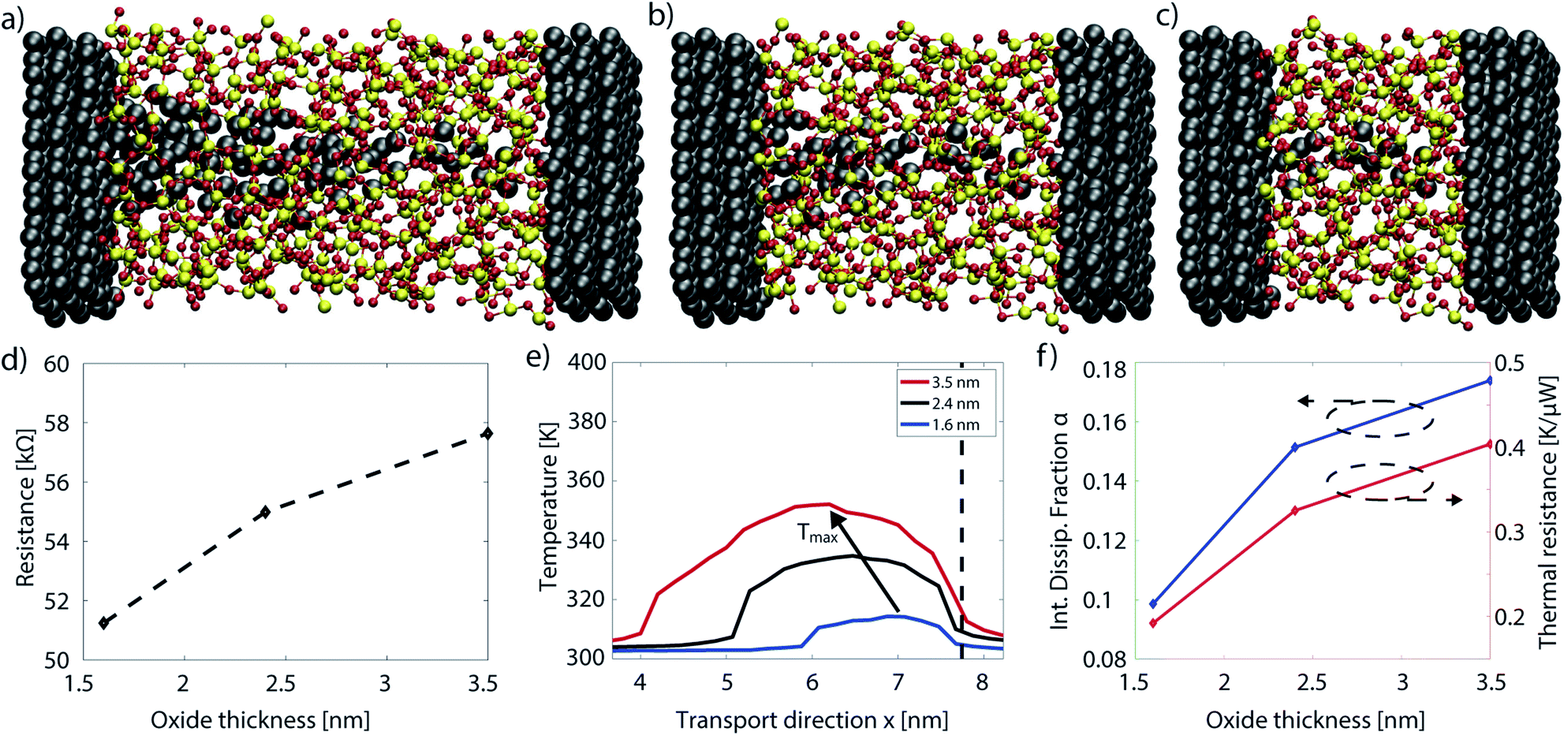 | ||
| Fig. 9 (a) CBRAM cell with an oxide length of 3.5 nm. (b) Same as (a), but with an oxide shortened from the left to 2.4 nm. The atomic configuration of the right-hand extremity of the filament is preserved. (c) CBRAM cell with an oxide layer shortened to 1.6 nm in the same fashion as (b). (d) Filament resistance as a function of the SiO2 layer thickness for an external bias of 0.2 V. The diamonds mark the simulated values, the dashed line serves as a guide to the eye. (e) Average temperature along the transport axis of the three CBRAM cells with different SiO2 layer thickness. For convenience, the filament tips are aligned at 7.6 nm. The vertical dashed line indicates the right device-electrode boundary. (f) Internal dissipation fraction α (left axis) and thermal resistance Rth (right axis) as a function of the SiO2 layer thickness. Subplots (a)–(c) and (e) are adapted from ref. 10, the data for (d) and (f) are presented in the ESI of ref. 10. | ||
As expected, the electrical resistance only slightly depends on the oxide thickness with a 10% reduction when going from the 3.5 nm to the 1.6 nm of a-SiO2 layer, as can be seen in Fig. 9(d). This confirms the assumption that the current is mostly limited by the filament extremity, not by its length. Consequently, self-heating can be compared between the three CBRAM cells using eqn (42), which depends on the current and resistance. The temperature averaged over the device cross-section is displayed in Fig. 9(e) for these three structures at an applied bias of 0.2 V. It is apparent that self-heating diminishes with the oxide thickness. Apart from a higher temperature profile in the thicker oxide, it can be noticed that the peak temperature moves further away from the contact towards the middle of the a-SiO2 layer.
The magnitude of the self-heating depends on two factors according to eqn (42): (1) the amount of power that is converted to heat (αRI2) and (2) the efficiency at which the excess phonon population can be extracted from the active region into the leads (Rth). To determine the origin of the increased temperature in thicker devices, both effects are examined separately. The internal power dissipation factor α versus the oxide thickness is plotted in Fig. 9(f). It can be observed that this quantity decreases with the oxide thickness. Hence, fewer phonons are emitted within the shorter cell. This behavior can be related to the time electrons spend propagating through the filament. The shorter the time, the lower the probability that an electron can interact with the surrounding lattice and dissipate energy.
To examine the thermal resistance of the device, Rth is drawn as a function of the oxide thickness, also in Fig. 9(f). We find that Rth exhibits the same characteristics as the power dissipation, i.e. Rth is smaller in thinner oxides: the phonons emitted by electrons remain longer in thicker oxides because they need more time to escape. The fact that copper is an excellent heat conductor whereas SiO2 is not, explains this behavior. As a result, the heat distribution is different in the three structures. The maximum temperature, which is located at the tip extremity in the shortest device, moves to the middle of the structure when the oxide thickness increases.
As both α and Rth increase with the oxide thickness, a strong dependence of self-heating on the dimensions of the switching layer is observed in the CBRAM cells. If we assume that excessive heating is the main reason for device failure, the experimental findings of ref. 10 can be readily explained: devices with a shorter oxide layer can endure larger currents before reaching the breakdown temperature. Stated differently, at a given current magnitude, self-heating is more pronounced in CBRAM cells with longer filaments because more phonons are emitted and they have more difficulties leaving the amorphous oxide region and attain the metallic contacts.
3.3 CBRAM simulations with different metal–oxide interfaces
In the CBRAM cells studied so far, both metal contacts were made of the same atom type as the filament. This is in contrast to real devices which feature an asymmetrical contact configuration. The approximation to use the same active metal for both electrodes facilitates the structure construction and reduces the computational burden. The impact of this approximation on the device characteristics has been analyzed in ref. 95. The main findings are summarized in this section, where different metals as the counter CBRAM electrode are examined. A new cell must be assembled for that purpose following the same procedure as described in Section 3.1. The active electrode and the filament are composed of Ag atoms, while three different metals are used for the counter electrode, namely Ag, Pt, and W. It is important to note that the atomic filament configuration remains identical, regardless of the counter electrode. The aim of this study is to determine how a different electrode may affect the current, which requires that the atomic configuration in the oxide layer does not change. In reality, the choice of the electrode is likely to modify the shape of the filament, but this is not the subject of the present study.Constructing a CBRAM cell where one electrode is different from the other requires special treatment due to the breaking of the structure symmetry along the transport axis. Two metals have different lattice constants in general, which creates a mismatch between the end of the right electrode (Ag in Fig. 10(a)) and the beginning of the left electrode (Ag, Pt, or W in our case). The electrodes can be strained to eliminate the lattice difference. To minimize its impact on the results, the metal supercells that build the left and right contacts should be chosen such that their dimensions match closely. To do that, a cross-section of 2.5 × 2.4 nm2 was selected. It ensures that the strain level does not exceed 1% for each electrode. The amorphous SiO2 does not have a lattice constant and hence does not suffer from strain. After setting up the Ag/a-SiO2/Ag structures, a conical Ag filament is inserted manually into the 2 nm thick oxide layer. The whole system is annealed with AIMD so that the filament displays an hourglass shape with a large cone on the counter electrode and a small one on the active electrode side, as shown in Fig. 10(a). The Pt and W electrodes are inserted after the atomic structure was optimized and annealed. One of the Ag electrodes is stripped away and replaced by either metal. Afterwards, the interface between the new metal and the oxide is optimized, while the bulk of the SiO2 and the right Ag electrode remain unchanged. In this way three material stacks with the same atomic filament are obtained. Next, the Hamiltonian and overlap matrices of each configuration are computed to perform ballistic electron transport calculations. Phonons and electron–phonon scattering are not considered here.
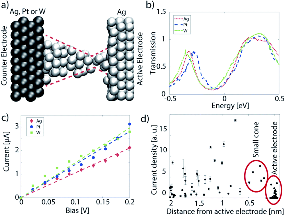 | ||
| Fig. 10 (a) Atomic configuration of a CBRAM cell with two different electrodes and an hourglass filament. White spheres represent silver atoms, the black ones tungsten. The red dashed line delimits the shape of the filament with a large cone on the left and a small one on the silver electrode. (b) Energy-resolved transmission as a function of the energy for the structures illustrated in (a) with Ag (red dotted), Pt (blue dashed), and W (green dash-dotted) as counter electrodes. (c) I–V characteristics of the three devices in (a) with Ag (red diamond), Pt (blue circles), and W (green squares) as counter electrodes. Linear fits are provided for convenience (dashed lines). (d) Current magnitude on the individual silver atoms in the filament and on the surface of the active electrode (black squares). The error bars give a measure of the variance of the current between the three structures. The atoms belonging to the active electrode and the small cone attached to it are indicated by the red circles. Subplots (a)–(d) are adapted from ref. 95. | ||
The energy-resolved transmission function around the Fermi energy is very similar in all CBRAM cells. It is reported in Fig. 10(b). This means that the probability of electrons of being transmitted through the oxide layer is independent of the contact material. In ballistic simulations the current is directly related to the transmission through eqn (17). Therefore, the I–V characteristics also resemble each other, Fig. 10(c), and confirm that the device current is mostly unaffected by the choice of the electrode metal.
Other than the current magnitude, its distribution can also play an important role in determining the device operation. To asses this quantity, the current vector starting from each atom is computed. The expression for that can be inferred from eqn (18): instead of summing all flows, each individual contribution is recorded and stored in the form of a current vector field. The current magnitude passing through each individual filamentary Ag and electrode surface atom is plotted in Fig. 10(d). The dots refer to the mean value between the three simulations and the error bar measures the standard deviation. Two distinct regimes can be discerned: (1) in the small cone situated on the active electrode, there is no variation in the current between the different structures; (2) some Ag atoms situated inside the large cone attached to the counter electrode (Ag, Pt, W) show a large spread in current. From these results, it can be deduced that the nature of the {Ag, Pt, W}-Ag filament influences the current distribution, but not its magnitude. The latter is determined by the thinnest region of the filament. In other words, the filament resistance depends on its atomic morphology. The current density, on the other hand, is affected by the interface connecting the counter electrode and the filament. Therefore, simulations considering two identical metal electrodes correctly predict the device resistance, but not the spatial distribution of the current. Electro-thermal effects, for instance, strongly depend on the current density, not only on its magnitude. In future work, the atomically resolved temperature of the three investigated CBRAM cells should be calculated to identify possible failure mechanisms.
4 Challenges and opportunities
The modeling techniques presented in this review paper come with heavy computational burden. To achieve a reasonable time-to-solution, while maintaining the used computing resources at a low level, different strategies can be applied. They can be loosely divided into two distinct and complementary categories. The first one consists of introducing physical approximations that reduce the computational complexity of the underlying algorithm. Opportunities are discussed here to circumvent these approximations without a large computational penalty. The second category considers improvements in the computational algorithms themselves, as well as in their parallelization. Such approaches are often independent from the physical models. More efficient algorithms may allow for the incorporation of previously unavailable physical principles.Approximations to the laws of quantum mechanics are the most challenging ones to address. They permeate the ab initio modeling and its most common form, DFT. The underestimation of the band gap is a known issue. Possible improvements include the use of hybrid functionals that can nowadays be applied even to large atomic systems.102 The HSE06 functional,103 for example, improves the description of the electronic structures, but it does not eliminate all problems. Further research towards more accurate and general exchange–correlation functionals is on-going.104 A related approximation mentioned in this review is the reduction of the calculations to the Γ-point. Because of the large size of the systems, a sparse k-point sampling is sufficient, but not optimal. With increasing available computational power and growing system sizes, the Γ-point limitation will become less prominent as the sampling of the momentum space implicitly increases with the simulation domain.
Improvements can also be brought on the phonon side where the dynamical matrix is often computed from force-fields for large systems. The main challenge to apply DFT is the huge number of force evaluations that are necessary. It scales linearly with the number of atoms, Natom, in addition to the typical O(Natom3) dependence of DFT itself. The fact that the response to the displacement of a single atom is localized could be exploited to develop a scheme where multiple, “far” away from each other, displacements are accounted for in a single force evaluation. This could considerably reduce the computational burden. The same considerations hold true for the calculation of the electron–phonon scattering elements. Instead of calculating them with a very basic model that only includes bond stretching and might neglect important effects the same methodology as for phonons could be used, with the same numerical challenges to overcome.
Within NEGF, generally, only local scattering events are accounted for. The off-diagonal entries of the scattering self-energies are discarded to reduce the computational complexity. To go one step further, the widely used RGF algorithm should be extended to produce the off-diagonal elements of the Green’s function, which are required to calculate other than diagonal components of the scattering self-energies. The computation of these entries becomes more and more difficult as one moves away from the diagonal. Improving the description of the scattering mechanism is definitively possible, but computationally very demanding. If experimental or reference data are available, it is preferable to scale the diagonal entries of the scattering self-energies with a constant factor to reproduce the desired targets.105 Note that additional effects such as anharmonic phonon–phonon interactions might be important. Including them would further increase the computational cost by slowing down the convergence of the SCBA iterations. Moreover, the matrix elements for anharmonic phonon–phonon scattering are related to the second derivatives of the forces acting on the atoms. Obtaining these derivatives is computationally even more challenging than the calculation of the dynamical matrix. Similar considerations as above could render these computations more affordable as long as small systems are investigated.
In terms of parallelization of the workload on high performance computing (HPC) resources solving the NEGF equations in the ballistic limit is an optimally suited problem as all energies (and momentum points in periodic structures) are independent from each other. As such, they can be naturally distributed to different computing units with little to no communication overhead in between. This picture completely changes when considering electron–phonon scattering where all energies (and momenta) are coupled. Recent advances in data-centric programming have shown that great speed-ups can be achieved if the parallelization is done based on the nature of the problem instead of physical intuitions.66 Another active research area is the development of so-called low-dimensional approximations, which drastically reduce the size of the Hamiltonian and overlap matrices in eqn (5).106 Such approximations can achieve cost reductions of multiple orders of magnitude with very little errors in the results. Presently, these approximations suffer from the requirement of devices made of the repetitions of identical cells. This is inherently incompatible with disordered structures as encountered in the oxide layer of RRAMs. Moreover, fully coupled electron–phonon simulations have yet to be demonstrated, when a low-dimensional basis is used. Nevertheless, if successful, such schemes could drastically change the size of the devices that can be simulated with NEGF at the ab initio level.
5 Conclusion
An overview on current state-of-the-art atomistic device simulation approaches has been presented in this paper. Techniques ranging from the construction of atomistic device configurations to dissipative quantum transport simulations have been discussed with a focus on the coupling of DFT with NEGF and the influence of electron–phonon interactions. To begin with, the working principle of emerging non-volatile memories has been introduced and the need for atomic device models highlighted. Force-field approaches have been identified as attractive options to describe thermal properties, whenever relevant parameters are available. Such models have been used together with ab initio electronic structure calculations to extract electro-thermal effects at the quantum mechanical level. The equations describing such high level approaches have been examined in detail, starting with the open-boundary conditions up to the inclusion of scattering mechanisms. Subsequently, the strength of the electro-thermal modeling environment has been illustrated with three case studies on the basis of conductive bridging random access memory cells. The importance of electron–phonon interactions have been demonstrated with emphasis on self-heating effects. The latter affect the breakdown behavior of nanoscale filaments by locally raising the temperature of few atoms.Limitations of the current methodology have been presented, together with opportunities for improvements. Many challenges remain to be tackled to enable fully ab initio dissipative quantum transport simulations of large-scale nanostructures. Most of them revolve around the computational cost of the DFT calculations that provide input parameters to the NEGF framework. Nevertheless, the demonstrated modeling platform combining first-principle calculations with force-field methods is already very powerful and can provide valuable insights into the physics and operation of nanodevices.
Conflicts of interest
There are no conflicts to declare.Acknowledgements
This work was supported by the Werner Siemens Stiftung, by ETH Research Grant ETH-35 15-2, and by a grant from the Swiss National Supercomputing Centre (CSCS) under Project s714 and s971.Notes and references
- A. Chaudhry and J. N. Roy, Semicond. Sci. Technol., 2010, 10, 20–27 CrossRef.
- M. Li, Sci. China: Phys., Mech. Astron., 2012, 55, 2316–2325 Search PubMed.
- T. Grasser, T.-W. Tang, H. Kosina and S. Selberherr, Proc. IEEE, 2003, 91, 249 CrossRef.
- A. Stukowski, Modell. Simul. Mater. Sci. Eng., 2012, 20, 045021 CrossRef.
- A. Chen, Solid-State Electron., 2016, 125, 25–38 CrossRef CAS.
- R. Waser, R. Dittmann, C. Staikov and K. Szot, Adv. Mater., 2009, 21, 2632–2663 CrossRef CAS.
- D. Ielmini, Semicond. Sci. Technol., 2016, 31, 063002–063027 CrossRef.
- E. Ambrosi, P. Bartlett, A. I. Berg, S. Brivio, G. Burr, S. Deswal, J. Deuermeier, M. A. Haga, A. Kiazadeh, G. Kissling, M. Kozicki, C. Foroutan-Nejad, E. Gale, Y. Gonzalez-Velo, A. Goossens, L. Goux, T. Hasegawa, H. Hilgenkamp, R. Huang, S. Ibrahim, D. Ielmini, A. J. Kenyon, V. Kolosov, Y. Li, S. Majumdar, G. Milano, T. Prodromakis, N. Raeishosseini, V. Rana, C. Ricciardi, M. Santamaria, A. Shluger, I. Valov, R. Waser, R. Stanley Williams, D. Wouters, Y. Yang and A. Zaffora, Electrochemical metallization ReRAMs (ECM) - Experiments and modelling: General discussion, Faraday Discuss., 2019, 213, 115–150 RSC.
- L. Bellaiche and D. Vanderbilt, Phys. Rev. B: Condens. Matter Mater. Phys., 2000, 61, 7877–7882 CrossRef CAS.
- B. Cheng, A. Emboras, Y. Salamin, F. Ducry, P. Ma, Y. Fedoryshyn, S. Andermatt, M. Luisier and J. Leuthold, Commun. Phys., 2019, 2, 1–9 CAS.
- W. Kohn and L. J. Sham, Phys. Rev., 1965, 140, A1133–A1138 CrossRef.
- L. P. Kadanoff and G. A. Baym, Quantum statistical mechanics: Green’s function methods in equilibrium and nonequilibirum problems, Benjamin, New York, 1962 Search PubMed.
- J. Taylor, H. Guo, J. Wang, T. Jeremy, H. Guo, J. Wang, J. Taylor, H. Guo and J. Wang, Phys. Rev. B: Condens. Matter Mater. Phys., 2001, 63, 1–13 Search PubMed.
- M. Brandbyge, J. L. Mozos, P. Ordejón, J. Taylor and K. Stokbro, Phys. Rev. B: Condens. Matter Mater. Phys., 2002, 65, 1654011–16540117 CrossRef.
- T. Frederiksen, M. Brandbyge, N. Lorente and A. P. Jauho, Phys. Rev. Lett., 2004, 93, 256601 CrossRef.
- S. Menzel, U. Böttger, M. Wimmer and M. Salinga, Adv. Funct. Mater., 2015, 25, 6306–6325 CrossRef CAS.
- S. Clima, B. Govoreanu, M. Jurczak and G. Pourtois, Microelectron. Eng., 2014, 120, 13–18 CrossRef CAS.
- J. Joshua Yang, F. Miao, M. D. Pickett, D. A. Ohlberg, D. R. Stewart, C. N. Lau and R. S. Williams, Nanotechnology, 2009, 20, 215201 CrossRef CAS.
- A. O’Hara, G. Bersuker and A. A. Demkov, J. Appl. Phys., 2014, 115, 183703 CrossRef.
- S. R. Bradley, A. L. Shluger and G. Bersuker, Phys. Rev. Appl., 2015, 4, 064008 CrossRef.
- A. Padovani, D. Z. Gao, A. L. Shluger and L. Larcher, J. Appl. Phys., 2017, 121, 155101 CrossRef.
- M. Schie, S. Menzel, J. Robertson, R. Waser and R. A. De Souza, Phys. Rev. Mater., 2018, 2, 035002 CrossRef CAS.
- J. J. Yang, M. D. Pickett, X. Li, D. A. Ohlberg, D. R. Stewart and R. S. Williams, Nat. Nanotechnol., 2008, 3, 429–433 CrossRef CAS PubMed.
- C. Funck, A. Marchewka, C. Bäumer, P. C. Schmidt, P. Müller, R. Dittmann, M. Martin, R. Waser and S. Menzel, Adv. Electron. Mater., 2018, 4, 1800062 CrossRef.
- K. Patel, J. Cottom, M. Bosman, A. J. Kenyon and A. L. Shluger, Microelectron. Reliab., 2019, 98, 144–152 CrossRef CAS.
- C. Wang, H. Wu, B. Gao, T. Zhang, Y. Yang and H. Qian, Microelectron. Eng., 2018, 187–188, 121–133 CAS.
- S. Menzel, J. Comput. Electron., 2017, 16, 1017–1037 CrossRef CAS.
- W. Wang, M. Laudato, E. Ambrosi, A. Bricalli, E. Covi, Y. H. Lin and D. Ielmini, IEEE Trans. Electron Devices, 2019, 66, 3795–3801 CAS.
- W. Wang, M. Laudato, E. Ambrosi, A. Bricalli, E. Covi, Y. H. Lin and D. Ielmini, IEEE Trans. Electron Devices, 2019, 66, 3802–3808 CAS.
- W. Wang, M. Wang, E. Ambrosi, A. Bricalli, M. Laudato, Z. Sun, X. Chen and D. Ielmini, Nat. Commun., 2019, 10, 81 CrossRef CAS PubMed.
- F. Ducry, A. Emboras, S. Andermatt, B. Cheng, J. Leuthold and M. Luisier, 2017 IEEE International Electron Devices Meeting (IEDM), 2017, pp. 83–86 Search PubMed.
- L. Zhao, S. G. Park, B. Magyari-Köpe and Y. Nishi, Appl. Phys. Lett., 2013, 102, 083506 CrossRef.
- W. M. Young and E. W. Elcock, Proc. Phys. Soc., London, 1966, 89, 735–746 CrossRef.
- L. Larcher and A. Padovani, J. Comput. Electron., 2017, 16, 1077–1084 CrossRef CAS.
- S. Menzel, P. Kaupmann and R. Waser, Nanoscale, 2015, 7, 12673–12681 RSC.
- S. Dirkmann and T. Mussenbrock, AIP Adv., 2017, 7, 065006 CrossRef.
- S. Dirkmann, J. Kaiser, C. Wenger and T. Mussenbrock, ACS Appl. Mater. Interfaces, 2018, 10, 14857–14868 CrossRef CAS PubMed.
- L. P. Wang, T. J. Martinez and V. S. Pande, J. Phys. Chem. Lett., 2014, 5, 1885–1891 CrossRef CAS PubMed.
- N. Onofrio, D. Guzman and A. Strachan, Nat. Mater., 2015, 14, 440–446 CrossRef CAS.
- E. A. Chagarov and A. C. Kummel, J. Chem. Phys., 2009, 130, 124717 CrossRef PubMed.
- A. C. Van Duin, S. Dasgupta, F. Lorant and W. A. Goddard, J. Phys. Chem. A, 2001, 105, 9396–9409 CrossRef CAS.
- A. K. Rappe and W. A. Goddard III, J. Phys. Chem., 1991, 95, 3358–3363 CrossRef CAS.
- S. C. Pandey, R. Meade and G. S. Sandhu, J. Appl. Phys., 2015, 117, 054504 CrossRef.
- X. Cartoixà, R. Rurali and J. Suñé, Phys. Rev. B: Condens. Matter Mater. Phys., 2012, 86, 165445 CrossRef.
- N. Onofrio, D. Guzman and A. Strachan, Nanoscale, 2016, 8, 14037–14047 RSC.
- K. Sankaran, L. Goux, S. Clima, M. Mees, J. A. Kittl, M. Jurczak, L. Altimime, G.-M. Rignanese and G. Pourtois, ECS Trans., 2012, 45, 317–330 CrossRef CAS.
- B. Xiao, X. F. Yu and J. B. Cheng, ACS Appl. Mater. Interfaces, 2016, 8, 31978–31985 CrossRef CAS.
- P. Hohenberg and W. Kohn, Phys. Rev., 1964, 136, B864 CrossRef.
- N. Mardirossian and M. Head-Gordon, Mol. Phys., 2017, 115, 2315–2372 CrossRef CAS.
- A. Kamenev, Field theory of non-equilibrium systems, Cambridge University Press, Cambridge, 2011, pp. 1–341 Search PubMed.
- J. Maassen, M. Harb, V. Michaud-Rioux, Y. Zhu and H. Guo, Proc. IEEE, 2013, 101, 518–530 Search PubMed.
- J. S. Wang, B. K. Agarwalla, H. Li and J. Thingna, Front. Phys., 2014, 9, 673–697 CrossRef.
- L. V. Keldysh, Sov. Phys. - JETP, 1965, 20, 1018–1026 Search PubMed.
- J. C. Slater and G. F. Koster, Phys. Rev., 1954, 94, 1498–1524 CrossRef CAS.
- C. Kittel, Introduction to Solid State Physics, Wiley, 8th edn, 2004 Search PubMed.
- N. D. Lang, Phys. Rev. B: Condens. Matter Mater. Phys., 1995, 52, 5335–5342 CrossRef CAS PubMed.
- GOLLUM, http://www.physics.lancs.ac.uk/gollum/ Search PubMed.
- TB_Sim, http://www.mem-lab.fr/en/Pages/L_SIM/Softwares/TB_Sim.aspx Search PubMed.
- NEMO5, https://engineering.purdue.edu/gekcogrp/software-projects/nemo5/ Search PubMed.
- G. Fiori and G. Iannaccone, NanoTCAD ViDES, 2008, https://nanohub.org/resources/vides Search PubMed.
- Siesta, https://departments.icmab.es/leem/siesta/ Search PubMed.
- QuantumATK version 2017.1, https://www.synopsys.com/silicon/quantumatk.html Search PubMed.
- R. Lake, G. Klimeck, R. C. Bowen and D. Jovanovic, J. Appl. Phys., 1997, 81, 7845–7869 CrossRef CAS.
- W. Lee, N. Jean and S. Sanvito, Phys. Rev. B: Condens. Matter Mater. Phys., 2009, 79, 085120 CrossRef.
- A. Afzalian and G. Pourtois, International Conference on Simulation of Semiconductor Processes and Devices, SISPAD, Sept. 1–4, 2019 Search PubMed.
- A. N. Ziogas, T. Ben-Nun, G. I. Fernández, T. Schneider, M. Luisier and T. Hoefler, The International Conference for High Performance Computing, Networking, Storage, and Analysis (SC’19), 2019, pp. 1–13 Search PubMed.
- T. Frederiksen, M. Paulsson, M. Brandbyge and A. P. Jauho, Phys. Rev. B: Condens. Matter Mater. Phys., 2007, 75, 1–22 Search PubMed.
- A. Gagliardi, G. Romano, A. Pecchia, A. Di Carlo, T. Frauenheim and T. A. Niehaus, New J. Phys., 2008, 10, 065020 CrossRef.
- N. Cavassilas, M. Bescond, H. Mera and M. Lannoo, Appl. Phys. Lett., 2013, 102, 10–13 CrossRef.
- H. Tian and G. H. Chen, Eur. Phys. J. B, 2013, 86, 411 CrossRef.
- M. R. Hirsbrunner, T. M. Philip, B. Basa, Y. Kim, M. Jip Park and M. J. Gilbert, Rep. Prog. Phys., 2019, 82, 046001 CrossRef CAS PubMed.
- E. Boström, M. Hopjan, A. Kartsev, C. Verdozzi and C. O. Almbladh, J. Phys.: Conf. Ser., 2016, 696, 012007 CrossRef.
- M. Bonitz, A. Filinov, J. W. Abraham, K. Balzer, H. Kählert, E. Pehlke, F. X. Bronold, M. Pamperin, M. Becker, D. Loffhagen and H. Fehske, Front. Chem. Sci. Eng., 2019, 13, 201–237 CrossRef.
- F. Bloch, Z. Phys., 1929, 52, 555–600 CrossRef.
- P. M. W. Gill, Adv. Quantum Chem., 1994, 25, 141–205 CrossRef CAS.
- L. W. Wang, Phys. Rev. B: Condens. Matter Mater. Phys., 2005, 72, 1–10 Search PubMed.
- A. Garcia-Lekue, M. G. Vergniory, X. W. Jiang and L. W. Wang, Prog. Surf. Sci., 2015, 90, 292–318 CrossRef CAS.
- N. Marzari, A. A. Mostofi, J. R. Yates, I. Souza and D. Vanderbilt, Rev. Mod. Phys., 2012, 84, 1419–1475 CrossRef CAS.
- A. Svizhenko, M. P. Anantram, T. R. Govindan, B. Biegel and R. Venugopal, J. Appl. Phys., 2002, 91, 2343–2354 CrossRef CAS.
- C. S. Lent and D. J. Kirkner, J. Appl. Phys., 1990, 67, 6353–6359 CrossRef.
- R. Haydock, Comput. Phys. Commun., 1980, 20, 11–16 CrossRef.
- S. Brück, Ph.D. thesis, ETH Zurich, 2017.
- M. Büttiker, Y. Imry, R. Landauer and S. Pinhas, Phys. Rev. B: Condens. Matter Mater. Phys., 1985, 31, 6207–6215 CrossRef PubMed.
- R. Rhyner and M. Luisier, Phys. Rev. B: Condens. Matter Mater. Phys., 2014, 89, 1–12 CrossRef.
- A. Togo, L. Chaput and I. Tanaka, Phys. Rev. B: Condens. Matter Mater. Phys., 2015, 91, 094306 CrossRef.
- M. Luisier, A. Schenk, W. Fichtner and G. Klimeck, Phys. Rev. B: Condens. Matter Mater. Phys., 2006, 74, 205323–205335 CrossRef.
- S. Brück, M. Calderara, M. H. Bani-Hashemian, J. VandeVondele and M. Luisier, J. Chem. Phys., 2017, 147, 074116 CrossRef.
- M. Luisier and A. Schenk, J. Comput. Theor. Nanosci., 2008, 5, 1031–1045 CrossRef CAS.
- P. Carbonniere, A. Dargelos and C. Pouchan, AIP Conf. Proc., 2007, 963, 329–336 CrossRef CAS.
- X. Gonze, Phys. Rev. A, 1995, 52, 1086–1095 CrossRef PubMed.
- C. Herring and E. Vogt, Phys. Rev., 1956, 101, 944–961 CrossRef CAS.
- H. Fröhlich, Adv. Phys., 1954, 3, 325–361 CrossRef.
- M. Luisier and G. Klimeck, Phys. Rev. B: Condens. Matter Mater. Phys., 2009, 80, 1–11 CrossRef.
- Á. Szabó, R. Rhyner and M. Luisier, Phys. Rev. B: Condens. Matter Mater. Phys., 2015, 92, 1–10 CrossRef.
- F. Ducry, K. Portner, S. Andermatt and M. Luisier, International Conference on Simulation of Semiconductor Processes and Devices (SISPAD), 2018, pp. 107–110 Search PubMed.
- S. Smidstrup, T. Markussen, P. Vancraeyveld, J. Wellendorff, J. Schneider, T. Gunst, B. Verstichel, D. Stradi, P. A. Khomyakov, U. G. Vej-Hansen, M. E. Lee, S. T. Chill, F. Rasmussen, G. Penazzi, F. Corsetti, A. Ojanperä, K. Jensen, M. L. Palsgaard, U. Martinez, A. Blom, M. Brandbyge and K. Stokbro, J. Phys.: Condens. Matter, 2020, 32, 015901 CrossRef CAS.
- J. Hutter, M. Iannuzzi, F. Schiffmann and J. VandeVondele, Wiley Interdiscip. Rev.: Comput. Mol. Sci., 2014, 4, 15–25 CAS.
- J. VandeVondele and J. J. Hutter, J. Chem. Phys., 2007, 127, 114105 CrossRef PubMed.
- E. S. Zijlstra, N. Huntemann, A. Kalitsov, M. E. Garcia and U. Von Barth, Modell. Simul. Mater. Sci. Eng., 2009, 17, 015009–015019 CrossRef.
- S. Goedecker, M. Teter and J. Hutter, Phys. Rev. B: Condens. Matter Mater. Phys., 1996, 54, 1703 CrossRef CAS PubMed.
- J. Perdew, K. Burke and M. Ernzerhof, Phys. Rev. Lett., 1996, 77, 3865–3868 CrossRef CAS PubMed.
- L. E. Ratcliff, A. Degomme, J. A. Flores-Livas, S. Goedecker and L. Genovese, J. Phys.: Condens. Matter, 2018, 30, 095901 CrossRef PubMed.
- A. V. Krukau, O. A. Vydrov, A. F. Izmaylov and G. E. Scuseria, J. Chem. Phys., 2006, 125, 224106 CrossRef.
- B. Kanungo, P. M. Zimmerman and V. Gavini, Nat. Commun., 2019, 10, 4497 CrossRef PubMed.
- R. Rhyner and M. Luisier, J. Appl. Phys., 2013, 114, 223708 CrossRef.
- M. Shin, W. J. Jeong and J. Lee, J. Appl. Phys., 2016, 119, 154505 CrossRef.
| This journal is © The Royal Society of Chemistry 2020 |