
 Open Access Article
 This Open Access Article is licensed under a Creative Commons Attribution-Non Commercial 3.0 Unported Licence
Assessing the role of plasma-engineered acceptor-like intra- and inter-grain boundaries of heterogeneous WS2–WO3 nanosheets for photocurrent characteristics†
Gopika
Gopakumar
,
Shantikumar V.
Nair
and
Mariyappan
Shanmugam
 *
*
Amrita Centre for Nanosciences and Molecular Medicine, Amrita Vishwa Vidyapeetham, Kerala-682041, India. E-mail: mshanmugham@aims.amrita.edu
First published on 22nd April 2020
Abstract
High-temperature annealing in tungsten disulfide resulted in heterogeneous WS2–WO3 in which intra- (within WS2 and WO3) and inter- (between WS2 and WO3) grain boundaries were observed, which were highly critical for charge transport and recombination. The heterogeneous WS2–WO3 phase was evidenced by observing the coexistence of d-spacing values of 0.26 nm (WS2) and 0.37 nm (WO3) in transmission electron microscopic (TEM) studies. Further systematic high-resolution TEM studies elucidated that intra-grain boundaries separated crystallites within WS2 and WO3, while inter-grain boundaries separated WS2 from WO3. As WS2 and WO3 are both n-type, these defects are acceptor-like in the grain boundaries and they actively participate in the capture (trapping) process, which impedes charge transport characteristics in the heterogeneous WS2–WO3 films. Plasma treatment in the heterogeneous WS2–WO3 film, for 60 minutes using argon, energetically modulated the defects in the intra/inter-grain boundaries, as evidenced from detailed comparative photocurrent characteristics obtained individually in (i) pristine WS2, (ii) heterogeneous WS2–WO3 and (iii) Ar plasma-treated heterogeneous WS2–WO3 films under blue and green lasers, along with AM1.5 (1 sun) illumination. Detrimental roles (trapping/de-trapping and scattering) of grain boundary states on photoelectrons were seen to be significantly suppressed under the influence of plasma.
Introduction
Graphene, with its two-dimensional (2D) layered structure, has been a wonder material, breaking technical limits on the applications of conventional functional materials in nanoelectronics, with new boundaries with exceptional structural, electrical and mechanical characteristics being established.1–3 The arrival of graphene into optoelectronic applications has opened up a highly challenging new technological era, in which multifarious 2D layered categories of semiconductors, metals and dielectrics have been explored.4–6 Tungsten disulfide (WS2) has been identified as a potential 2D-layered semiconductor, exhibiting a hexagonal honeycomb lattice structure, with a tunable optical band gap in the range of direct 1.8 eV (monolayer) to indirect 1.3 eV (bulk).7–10 Wet chemical methods, chemical vapor deposition (CVD) and micro-mechanical/chemical exfoliation techniques are well-known methods reported for the synthesis of WS2.11–15 It has been observed that exfoliation and CVD-based approaches yield good-quality WS2 with the possibility of precise control over the thickness (number of atomic layers).16,17 Recently, atomic layer deposition-based, atomically thin wafer-scale production of WS2 has been demonstrated, which allows the possibility of building large-area electronic networks based on nanofabrication.18–20In general, high-temperature processes or any other special treatment methods, such as UV–ozone, on WS2 cause dominant oxidation, resulting in the oxide phase coexisting in the same material along with the parent sulfide component.21 Photo-oxidation due to ambient light exposure for a week in WS2 films led to oxidation, specifically under excitation energies above the trion excitation energy.22 It has been observed that WS2 is highly stable below 350 °C but becomes sensitive at temperatures above 450 °C, at which WS2 is transformed into WO3, with further increase in thermal treatment causing significant changes in morphology as well.23 Photocatalytic activity in lateral heterostructures of WS2/WO3 has been reported and the study showed the possibility of achieving simultaneous interaction of oxygen with both sides in WS2via selective oxidation.24 The kinetics of the hydrogen evolution reaction were significantly improved using heterostructure hybrid catalysts based on WS2/WO3.25 It has recently been demonstrated, via the in situ anodic oxidation of a WS2 film, that a current density of 100 mA cm−2 at 152 mV was attributable to the excellent kinetics of the hydrogen evolution reaction.26 It has been observed that the presence of photocatalytic activity and photoresponsive behavior can be significantly improved by introducing WO3 in WS2, as the charge transport characteristics are improved.27 Azam et al. have reported electrochromic devices based on 2D WO3 obtained from the oxidation of 2D WS2 that showed 62.57% color modulation at a wavelength of 700 nm, which has been claimed to be approximately three times more than for bulk WO3.28 Recently, photovoltaic application of WS2 processed from WO3 was demonstrated as a counter electrode material resulting in 7.2% photoconversion efficiency.29 Our previous study demonstrated the photovoltaic effect in dye-sensitized 2D-layered WS2 films, which showed the coexistence of WS2 and WO3.30
In this work, a detailed structural, optical, and nanomorphological evolution of heterogeneous WS2–WO3 films is studied and their influences on photocurrent measurements performed under three different illuminations are presented. Charge transport characteristics in the heterogeneous WS2–WO3 films under dark and three different illuminations are explained in terms of the presence of the oxy-sulfide heterogeneous phase WS2–WO3, the two types of grain boundaries separating them and the associated defects within the boundaries. Finally, the effect of argon plasma interaction with WS2–WO3 films, and its consequences, are explained.
Experimental section
Pristine WS2 powder (99% purity, Alfa Aesar) was used to prepare a colloidal paste by mixing it with a polyester (99% purity, Sigma Aldrich) polymer solution. The colloidal paste was then doctor-bladed onto glass substrates (Corning) and annealed at 530 °C for 1 h. After the annealing process, the samples were allowed to cool to room temperature with no external influences. A crack-free, uniform WS2 thin-film coating was achieved, as illustrated in Fig. 1(a). The sample was further thermally treated and a significant change in color was observed representing WS2–WO3, as shown in Fig. 1(a). The sample was then subjected to argon (Ar) plasma for 60 minutes with a radiofrequency power of 10 W and a gas flow rate of 30 sccm. The plasma-treated sample is also shown at the bottom in Fig. 1(a).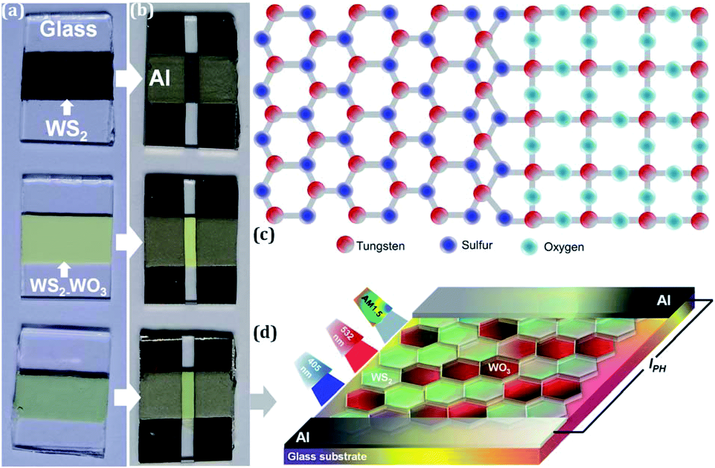 | ||
| Fig. 1 (a) Digital images of pristine WS2, heterogeneous WS2–WO3, and plasma-processed heterogeneous WS2–WO3. (b) Corresponding fabricated devices using Al as metal contacts. (c) Schematic illustration showing the coexistence of WS2 and WO3 in the crystal structure, giving heterogeneity. (d) Schematic of the fabricated two-terminal devices using heterogeneous WS2–WO3 as a photoactive material. | ||
Photocurrent measurements were performed on all three samples: (i) pristine WS2, (ii) heterogeneous WS2–WO3 and (iii) Ar plasma-treated heterogeneous WS2–WO3, by coating aluminum metal contacts using DC sputtering with a power of 50 W and Ar gas flow rate of 30 sccm. The aluminum electrode deposition was carried out for 30 minutes on the three samples, with a gap of 2 mm maintained by a shadow mask. The aluminum electrode-coated WS2, WS2–WO3 and plasma-processed WS2–WO3 devices are shown in Fig. 1(b). Fig. 1(c) shows a schematic illustration of the coexistence of WS2–WO3 in the samples illustrated in Fig. 1(a). The samples were then illuminated using three different light sources: (i) white light with AM1.5 photon flux, (ii) blue (405 nm) and (iii) green (532 nm) lasers to measure the current–voltage (I–V) characteristics, as shown in Fig. 1(d). Pristine WS2, WS2–WO3 and plasma-processed WS2–WO3 were used as charge transport channels along with aluminum metal contacts to inject/collect the charge carriers, like a source/drain.
Results and discussion
Fig. 2(a) shows the X-ray diffraction (XRD) patterns corresponding to pristine WS2, WS2–WO3 and plasma-processed WS2–WO3 films. The pristine WS2 showed peaks at 2θ values of 14.4°, 28.9°, 33.5°, 33.6°, 39.5°, 43.9° and 58.3°, corresponding to the indices (002), (004), (100), (101) (103), (006) and (110), respectively. These values were further matched with previously reported studies and it was observed that all were in good agreement.31,32 All the XRD peaks evidenced the presence of crystalline WS2, used as a source material for the preparation of the oxy-sulfide phase of WS2.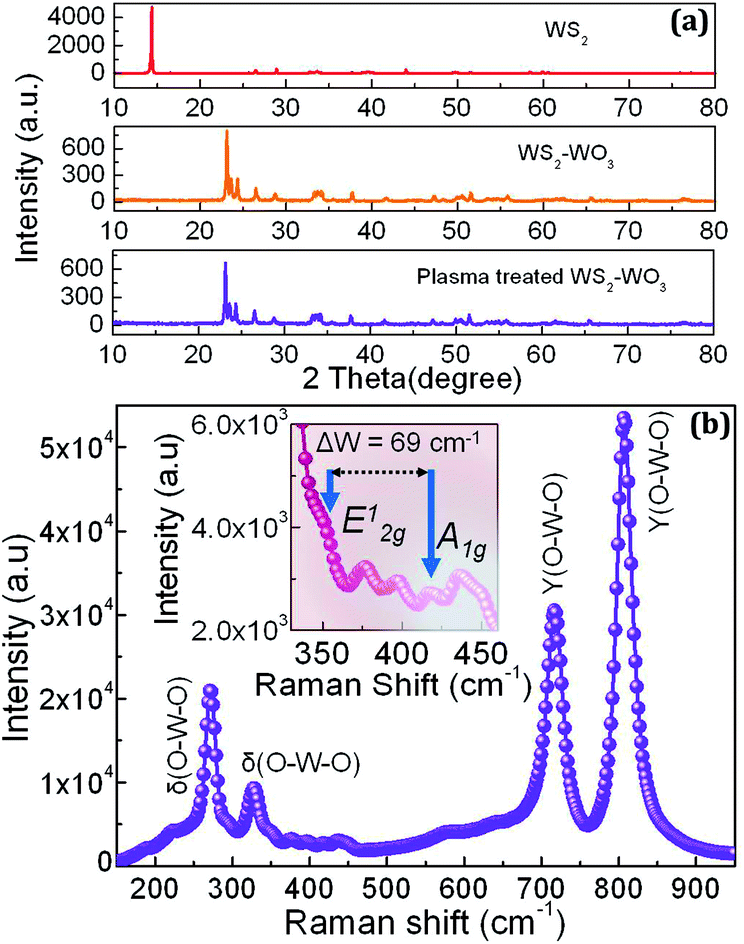 | ||
| Fig. 2 (a) XRD patterns obtained from pristine WS2, WS2–WO3 and plasma-treated WS2–WO3 films. (b) Raman spectrum obtained from the plasma-treated WS2–WO3 film. | ||
The peak at 14.4° indexed to (002) represents the stacked crystalline layers in the bulk WS2. The XRD pattern of the oxy-sulfide phase in WS2 (represented as WS2–WO3) showed the absence of the 14.4° peak, confirming the transformation of pristine WS2 into the mixed oxy-sulfide phase. In general, the XRD peak intensity is significantly affected by the exfoliation process, as the atomically thinner region is reached and the peak vanishes upon complete phase transformation, as evidenced from previously reported studies.31,33 The other major peaks were observed at 23.1°, 23.6°, 24.3°, 33.6° and 34.1° corresponding to the planes (002), (020), (200), (022) and (201), respectively. These crystalline peaks represent the presence of monoclinic WO3, as reported elsewhere.34 Due to the relatively lower amount of WS2 in WO3, the characteristic XRD peaks of WS2 were not observed. It has already been reported that the absence of peaks due to lower concentration, in terms of phase fraction, is relatively common in 2D-layered van der Waals materials.35–37 The XRD pattern of the plasma-treated oxy-sulfide phase in WS2 was observed to be very similar to the XRD pattern of WS2–WO3. This confirmed that plasma treatment did not change the crystallographic nature of the WS2–WO3. Moreover, it was also realized that the presence of the WS2–WO3 phase in WS2 is highly stable, and could not be altered by the low power argon plasma used in the present study.
Fig. 2(b) shows the Raman-active modes observed in the plasma-processed WS2–WO3 sample. WO3 exhibited high intensity modes compared with WS2, which showed low intensity Raman modes. The bending vibrations belong the O–W–O bonds observed at 271.1 and 327.1 cm−1 are denoted as δ(O–W–O). The stretching of the O–W–O bonds observed at 716.7 and 806.6 cm−1 is represented as γ(O–W–O). Both bending and stretching vibrational modes are specific for the monoclinic WO3 structure.28,38,39 WS2 exhibited in-plane A1g and out of plane E12g vibrational modes, as shown in the inset. E12g appeared as a shoulder peak at the high intensity Raman mode of WO3, as a result of which the difference in peak intensity between E12g and A1g is not very clear. The frequency difference, Δw, between the two modes of WS2 is directly related to its thickness. If Δw is 70 cm−1, then it represents the bulk, and values less than this are considered to indicate the presence of a monolayer, bilayer and trilayer.40 In the case of the WS2 oxy-sulfide phase, Δw was found to be ∼69 cm−1, indicating the presence of a few layers in WS2. Atmospheric oxygen intercalated into the WS2 sheets while undergoing high-temperature annealing and reacted with tungsten in the surface defects forming the oxy-sulfide phase in WS2. The other Raman modes, shown in the inset at 376.8 and 435.9 cm−1, represent vibrations due to γ(W–OH2) and δ(O–W–O) in WO3 respectively. The γ(W–OH2) vibration could be due to water molecules present at the surface of the WO3, as the characterization was carried out under atmospheric conditions.41
Fig. 3 shows three rows of scanning electron microscopy images obtained from pristine WS2 (row 1), heterogeneous WS2–WO3 (row 2) and plasma-treated WS2–WO3 (row 3). The difference between the three columns is just in the magnification, as 5000×, 10![[thin space (1/6-em)]](https://www.rsc.org/images/entities/char_2009.gif) 000× and 20000×. All three films exhibited randomly distributed platelet structures. The platelets were micrometers in size with dominant hexagonal shapes, as can be seen from the 20000× images (column 3). In the case of pristine WS2 film, the hexagonal platelets were observed to be smooth with sharp edges. In the case of the heterogeneous WS2–WO3 film, the precise hexagonal feature in the platelets was altered. This effect was even more significant in the case of plasma-treated WS2–WO3 film, as can be seen from row 3. It is clear that argon plasma energetically diffused into the randomly distributed hexagonal platelets and altered the distribution and surface smoothness, as can be clearly seen at 20000×.
000× and 20000×. All three films exhibited randomly distributed platelet structures. The platelets were micrometers in size with dominant hexagonal shapes, as can be seen from the 20000× images (column 3). In the case of pristine WS2 film, the hexagonal platelets were observed to be smooth with sharp edges. In the case of the heterogeneous WS2–WO3 film, the precise hexagonal feature in the platelets was altered. This effect was even more significant in the case of plasma-treated WS2–WO3 film, as can be seen from row 3. It is clear that argon plasma energetically diffused into the randomly distributed hexagonal platelets and altered the distribution and surface smoothness, as can be clearly seen at 20000×.
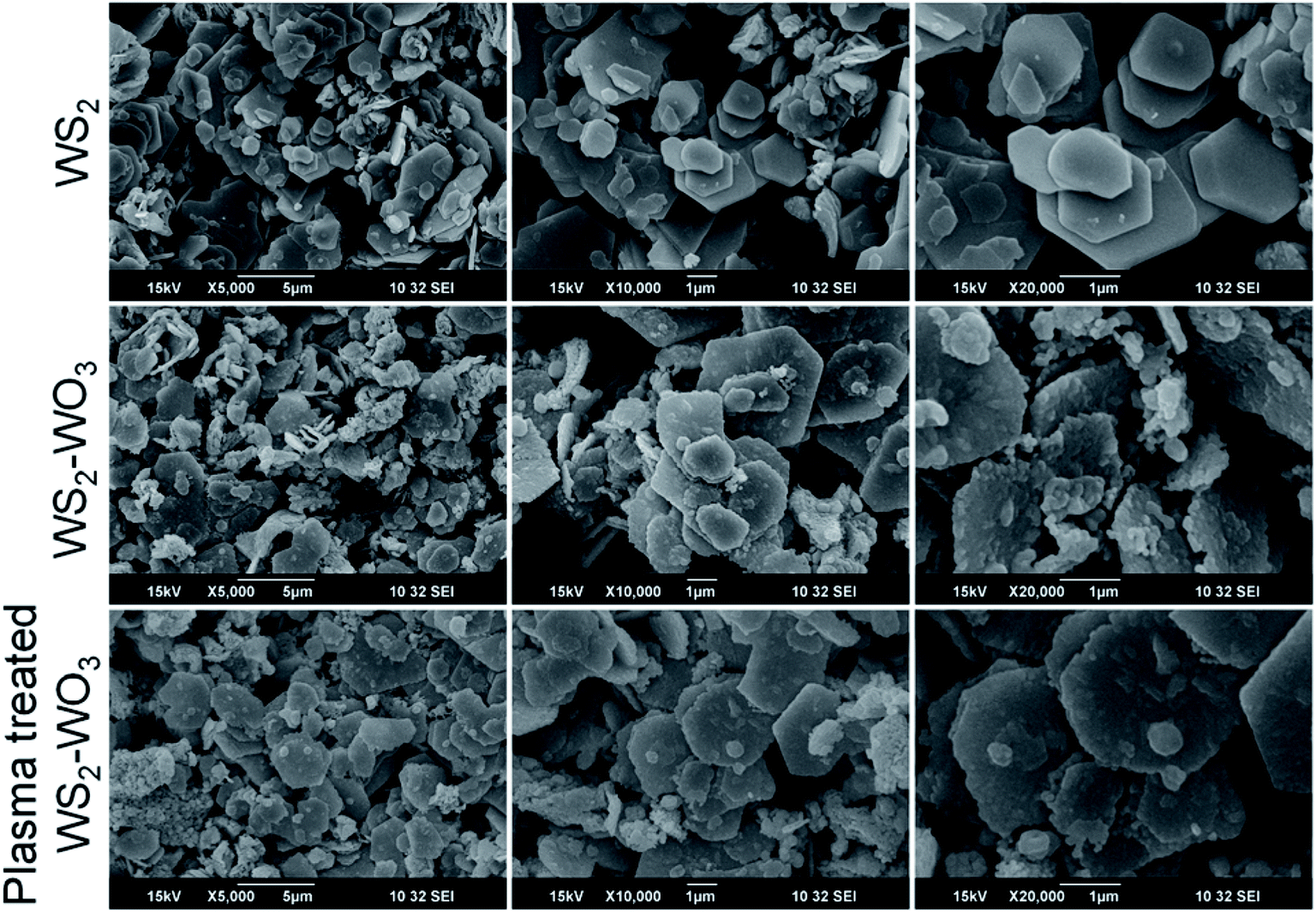 | ||
| Fig. 3 Surface morphology of pristine WS2 (row 1), heterogeneous WS2–WO3 (row 2) and plasma-treated WS2–WO3 (row 3). | ||
The high-resolution transmission electron microscopy (HR-TEM) images shown in Fig. 4(a)–(f) were used to analysis and explain the concepts of inter- and intra-grains along with boundaries. Fig. 4(a) shows a well-defined intra-grain boundary (within the same phase) in WO3, as confirmed via the d-spacing of 0.37 nm. The grain boundary that separates the two grains in WO3 is marked with yellow dotted lines. Fig. 4(b) illustrates the inter-grain boundaries (between different phases) separating the WS2 from WO3, as evidenced by the d-spacing values of 0.26 and 0.37 nm, respectively.
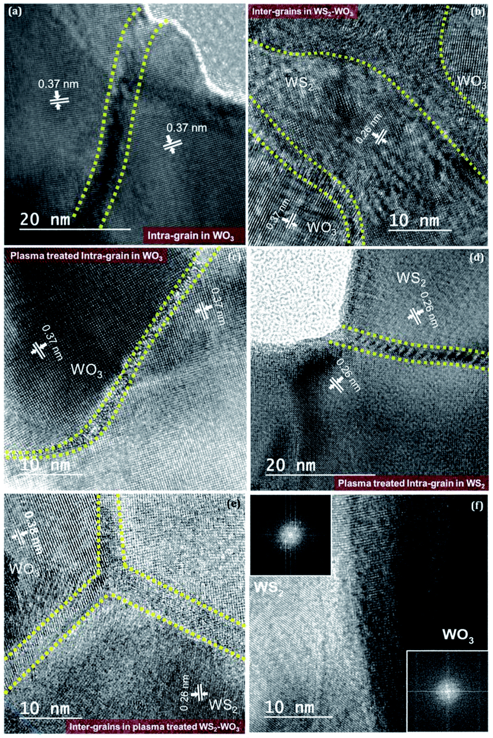 | ||
| Fig. 4 HR-TEM images showing the evolution of (a) intra-grain boundary in WO3, (b) inter-grain boundary in WS2–WO3, (c) intra-grain boundary in WO3 after plasma treatment, (d) intra-grain boundary in WS2 after plasma treatment, (e) inter-grain boundary in WS2–WO3 after plasma treatment and (f) FFT shows the presence of inter-grain boundary separating WS2 and WO3. | ||
Plasma treatment in the heterogeneous WS2–WO3 film showed that the boundaries were sharpened, with not much spread into the grains, as shown in Fig. 4(c) and (d). This can be attributed to the plasma energy facilitating increased grain size distribution, which eventually reduced the grain boundaries. Fig. 4(c) shows the plasma-treated intra-grain boundary separating two WO3 grains, but the boundary is observed to be sharper compared with the sample without plasma treatment. Fig. 4(d) shows the plasma-treated intra-grain boundary corresponding to WS2 grains, as confirmed by the d-spacing of 0.26 nm. Fig. 4(e) and (f) depict the inter-grain boundaries isolating WS2 and WO3 very precisely. Fast-Fourier transform analysis further verified the presence of an inter-grain boundary separating WS2 and WO3 abruptly, as shown in Fig. 4(f).
Fig. 5 shows the UV-visible absorbance spectra of the WS2 oxy-sulfide phase with and without plasma treatment in the wavelength range 350–800 nm. The inset shows the absorbance spectrum of exfoliated WS2 sheets. The absorbance spectra of the oxy-sulfide phase of WS2 showed a broad absorbance due to the coexistence of WO3 and WS2 in the sample. WO3, with a band gap of 2.7 eV, showed some photo-absorption in the visible spectrum, which is consistent with previous studies.42,43 Optical absorbance of WS2 is highly tunable and is sensitive to many factors, such as number of layers,44 defects,45–47 and strain.48,49 Defects in 2D-layered materials play a critical role in optical absorbance.46 In the case of the oxy-sulfide phase of WS2, the synthesis creates many defects associated with sulfur and oxygen. In addition, the presence of grains and grain boundaries also creates many defects, which affect the band gap of WS2.45–47
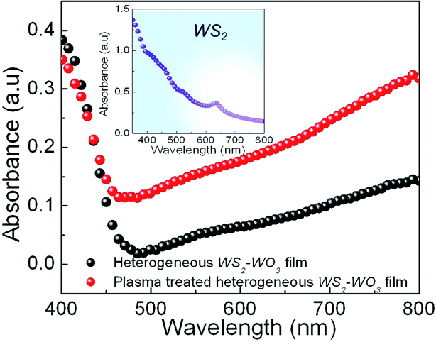 | ||
| Fig. 5 UV-visible optical absorbance spectra of heterogeneous WS2–WO3 film before and after plasma treatment, with the inset showing the absorbance of pristine WS2 film. | ||
Fig. 6 shows comparative I–V characteristics of (i) pristine WS2, (ii) heterogeneous WS2–WO3 and (iii) plasma-treated WS2–WO3 films. The measured I–V characteristics for all three samples were highly linear in an applied bias region of ±10 V. This first shows that all three samples formed a highly ohmic junction with aluminum contacts, which facilitated efficient charge transport through pristine WS2, heterogeneous WS2–WO3 and plasma-treated WS2–WO3 films. Fig. 6(a)–(d) specifically represents I–V characteristics obtained in the dark and under blue laser, green laser and AM1.5 illumination, respectively. The insets in all four categories represent just an expanded view of the WS2 and heterogeneous WS2–WO3 samples in an applied bias region of 0–10 V, as these were very close to each other and lower in comparison with the plasma-treated sample. Fig. 6(e) shows the energy band alignment in the heterogeneous WS2–WO3 films. Three potential barriers are illustrated as I, II and III. Barrier I situated in WO3 represents a potential disruption energy band structure within WO3. When multiple grains form together to make a thin film, it is obvious that grain boundaries are established within the phase and such boundaries can be considered as intra-grain boundaries. Similarly, the grain boundary within WS2 grains is represented in region III, with a possible interruption in the potential profile as illustrated. Interestingly, when two different phases coexist to form a heterogeneous material system, an inter-grain boundary is also established. The inter-grain boundaries create a potential barrier for charge transport at the interface of WS2/WO3. In general, defect-free single crystalline semiconductors are expected not to show such disorders in their energetics, but it is quite impossible to meet such criteria in a real case, as material synthesis and device fabrication processes involve several experimental difficulties that directly cause disorder in materials. In this case, both WS2 and WO3 are both n-type materials existing together and forming the heterogeneity with well-defined inter-grain boundaries. Grain boundaries, in general, possess lot of crystallographic defects, as the structural disorder predominantly occurs right at the interface between WS2 and WO3, as shown in region II in Fig. 6(e).
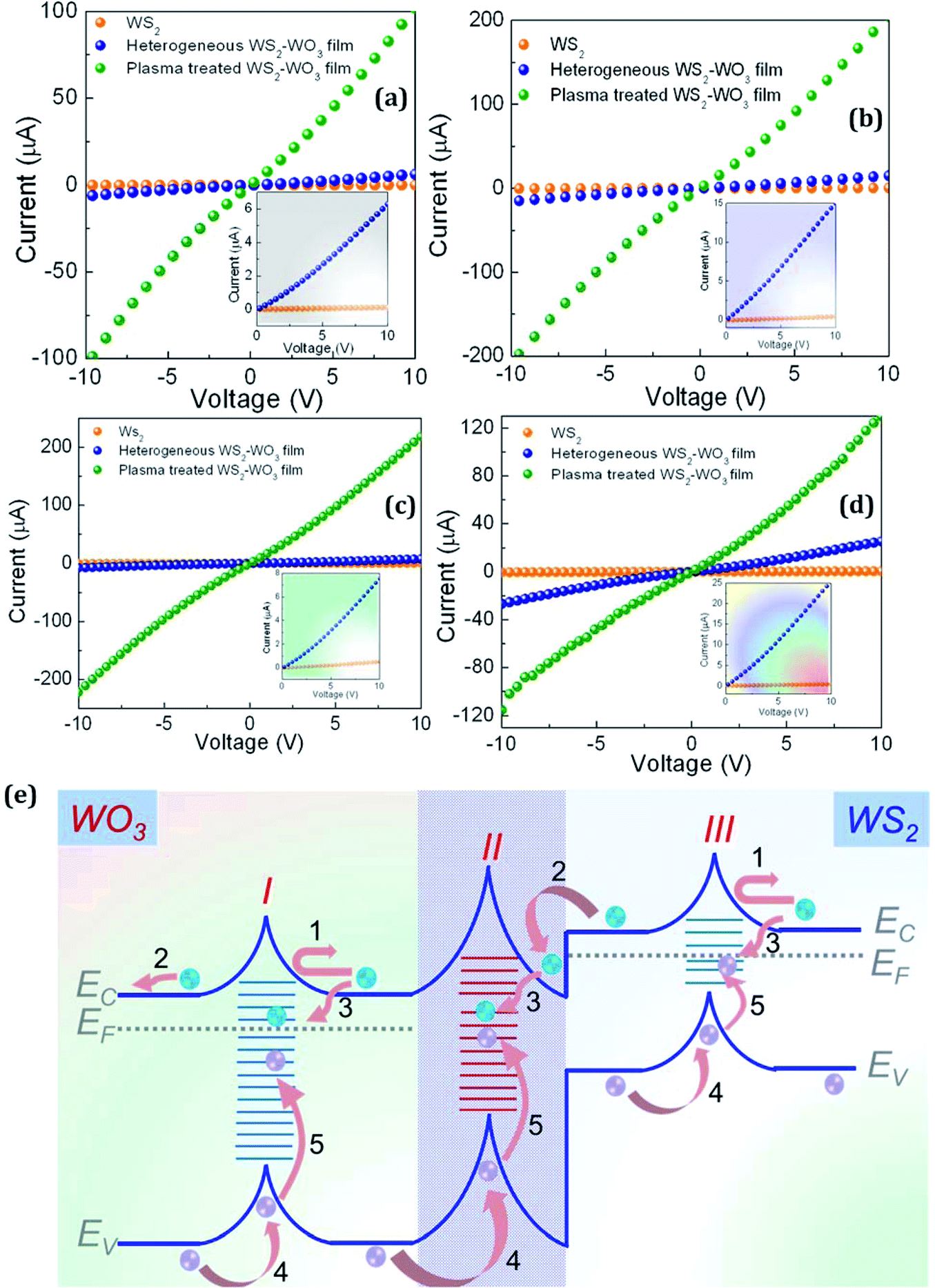 | ||
| Fig. 6 I–V characteristics of the pristine WS2, heterogeneous WS2–WO3 and plasma-treated WS2–WO3 measured under (a) dark, (b) blue laser illumination, (c) green laser illumination and (d) AM1.5 illumination. (e) Schematic illustration showing the presence of the inter-grain boundary between WS2–WO3 and the intra-grain boundary in WS2 and WO3 on potential distribution, with various physical processes interfering with charge transport and recombination dynamics. | ||
Charge transport and recombination dynamics in the heterogeneous WS2–WO3 are illustrated through the various processes listed (1)–(5). Optical excitation in WS2 generates a free electron and hole in conduction (EC) and valence (EV) band edges, respectively; processes (1). The free electron in the EC should move towards the EC of WO3 to stabilize, due to the position of the EC of WO3, which is a few meV below WS2. However, it has to pass through the structurally disordered region II, the inter-grain boundary, which separates WS2 from WO3via defect distribution as illustrated.
Grain boundaries are considered to be charged by majority carriers, in this case electrons, and to affect the band structure by creating potential barriers, as illustrated. Charge transport is impeded by such a potential barrier, as shown in process (2). Thus, photogenerated electrons can be trapped, process (3), in such defect states and attain localized distribution, which can effectively attract a hole from EV, as illustrated in processes (4) and (5). In general, the presence of defects in grain boundaries facilitates bringing photogenerated electrons and holes together (electron–hole capture) in the nanoscale range, at which point recombination becomes prominent. In this situation the defects in inter- and intra-grain boundaries act as acceptor-like states, which actively participate in electron capture, making them negatively charged. The negatively charged defects cause hole transport in the EV and eventually both electron and hole transport processes are affected. Plasma is an energetic environment, which can interact with functional materials to engineer structural and optoelectronic properties. This energetic environment is capable of passivating defects in the grain boundaries of materials and thus reduces their capability and probability for charge trapping. It also reduces the potential barriers in the intra- and inter-grain boundaries that were established due to the presence of defects. This influences the electron–hole capture in the trap states and effectively improves charge transport kinetics. The change in currents measured under different situations evidences the fact that defects at the grain boundaries and their activity on charge transport characteristics are controlled by plasma treatment.
Fig. 7(a) shows the photoresponsivity (current due to the exciton generation via light exposure) of the pristine WS2, heterogeneous WS2–WO3 and plasma-treated WS2–WO3 films. In order to represent a comparative plot for the photoresponsive characteristics of the three samples, an applied bias of 10 V was used. The increment in current values (δI) for pristine WS2, heterogeneous WS2–WO3 and plasma-treated WS2–WO3 films was calculated under AM1.5 photon flux, blue and green laser illuminations with respect to the current values measured under dark condition: as IEffective = IIllumination − IDark, where IEffective represents the photoresponsivity of the specific sample. In Fig. 7(a), the photoresponsivity of pristine WS2 was found to be very minimal under AM1.5 (0.30 μA) and blue laser (0.32 μA) illuminations, with a slight increase under green laser (0.41 μA) illumination. This is due to the bulk nature, since the WS2 layers were almost stacked while coating the films. The photoresponsivity values of the heterogeneous WS2–WO3 were found to be reduced in the case of blue (8.7 μA) and green (1.3 μA) laser illumination at an applied bias of 10 V, when compared with AM1.5 illumination (19.0 μA). This can be attributed to more active recombination sites in the material, due to the presence of defects. The photoresponsivity under green laser was reduced due to the presence of defects in the intra-grain boundaries in WS2 and WO3 and inter-grain boundaries between WS2 and WO3. After plasma treatment the effects of grain boundary defects on charge transport characteristics are minimized, which can be seen from the bar graph for plasma-treated WS2–WO3 film. The photoresponsivity under the green laser (116.7 μA) was enhanced most when compared to values under the blue laser (102.9 μA) and AM1.5 illumination (27.7 μA). All of these results showed the possibility of engineering grain boundary defects in heterogeneous WS2–WO3.
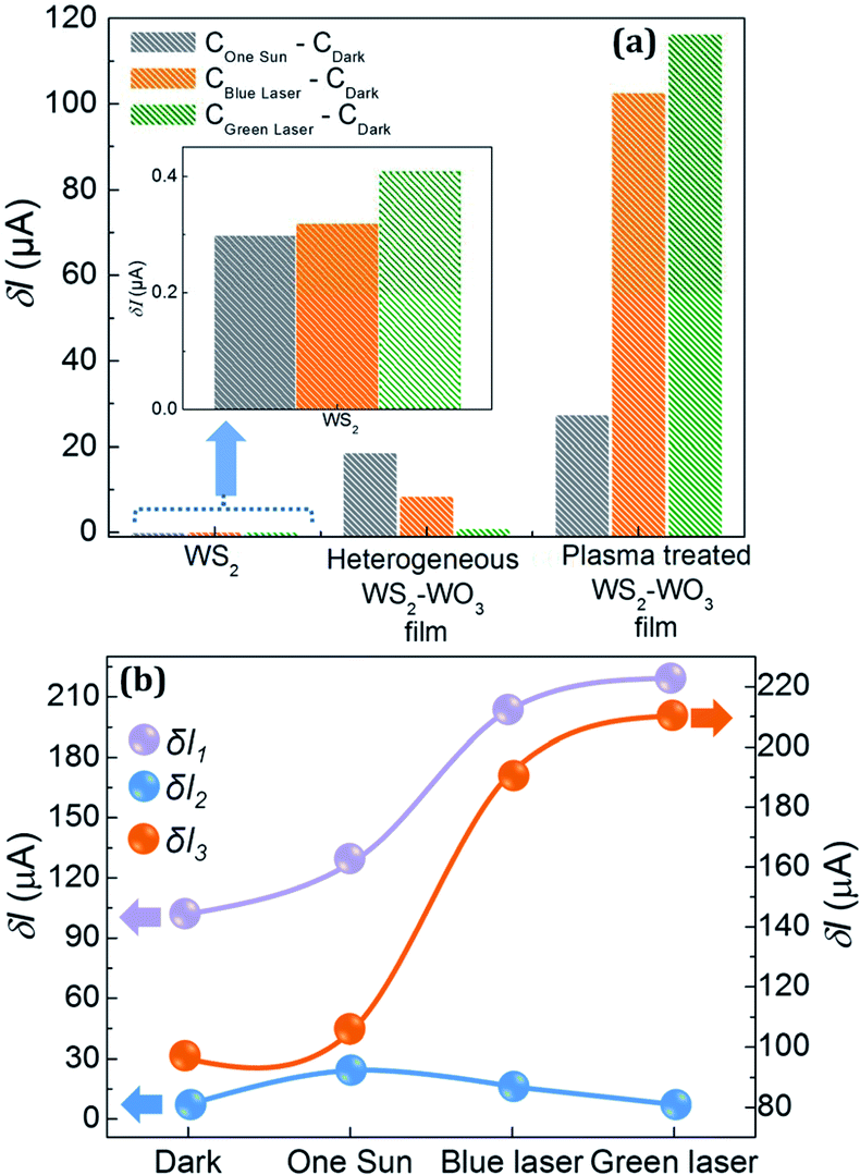 | ||
| Fig. 7 (a) Photoresponsivity of pristine WS2, heterogeneous WS2–WO3 and plasma-treated WS2–WO3 films at an applied bias of 10 V. (b) δI1 and δI2: increment in currents in heterogeneous WS2–WO3 and plasma-treated WS2–WO3 with respect to pristine WS2. δI3: increment in current of plasma-treated WS2–WO3 with respect to heterogeneous WS2–WO3. | ||
Fig. 7(b) shows the increase in current values measured in the pristine WS2, heterogeneous WS2–WO3 and plasma-treated WS2–WO3 films. The difference in current depicted for all three samples and all three illuminations under dark conditions are taken with the applied bias value of 10 V. In Fig. 7(b), δI1 and δI2 represent the increment in current in the case of heterogeneous WS2–WO3 and plasma-treated WS2–WO3 with respect to pristine WS2. δI3 represents the increase in the current of plasma-treated WS2–WO3 with respect to heterogeneous WS2–WO3. The arrows indicate the respective axes at which the change in current values was recorded. The δI1 values were 24.9 μA under one sun illumination, 14.6 μA under blue laser, and 7.0 μA under green laser illumination, along with 6.2 μA under dark conditions. This shows that the increase in the current occurred after formation of the heterogeneous WS2–WO3 phase in the pristine WS2. The increment in current values varied depending on the illumination conditions and sensitivity of the response of the material to incident energy. The δI2 values were 129.1 μA under one sun illumination, 204.2 μA under blue and 217.9 μA under green laser illumination, along with 101.6 μA under dark conditions. This shows that there was an increment in current, even more than δI1, after plasma treatment in the heterogeneous WS2–WO3 film. As in the case of δI1, the values of δI2 also varied depending on the illumination conditions and sensitivity of the photoresponse of the material. Contrary to δI1, values of δI2 showed a greater increase under blue and green lasers than under AM1.5 illumination. This can be attributed to the effective passivation of defect states associated with inter- and intra-grain boundaries by argon plasma treatment. Blue laser illumination is more interactive with the wide band gap of WO3, while interaction of photons from the green laser is more effective with WS2. Furthermore, δI3 represents the increment in current values of plasma-treated WS2–WO3 samples with respect to heterogeneous WS2–WO3. The δI3 values were 104.1 μA under one sun illumination, 189.6 μA under blue and 210.9 μA under green laser illumination, along with 95.5 μA under dark conditions. These values also showed an enhancement with respect to plasma treatment, suggesting the effective interaction of plasma with defects. These results showed that the photoresponse of heterogeneous WS2–WO3 was better than that of pristine WS2, and plasma treatment of heterogeneous WS2–WO3 could further improve the charge transport characteristics by achieving effective defect passivation.
Conclusion
It has been inferred that the presence of heterogeneity in functional semiconductors establishes grain boundaries within and between the heterointerfaces, through which charge transport occurs. Such electronically active boundaries, which influence charge transport at the nanoscale, can be engineered via energetically active plasma treatment. The plasma environment in heterogeneous semiconducting phases alters the optoelectronic characteristics, as evidenced by optical absorption and electrical transport studies, suggesting that it is highly suitable for defect engineering at the nanoscale level.Conflicts of interest
On behalf of all contributing authors, the corresponding author declares that there is no conflict of interest.Acknowledgements
The authors would like to thank Mr Sajin, Mr Dennis, and Ms Selvi for their help in various characterizations and Amrita Centre for Nanosciences for providing the PVD cluster facility through industry support for plasma and thin-film processing.References
- A. K. Geim, Science, 2009, 324, 1530–1534 CrossRef CAS PubMed.
- K. S. Novoselov, V. I. Fal, L. Colombo, P. R. Gellert, M. G. Schwab and K. Kim, Nature, 2012, 490, 192 CrossRef CAS PubMed.
- A. C. Ferrari, F. Bonaccorso, V. Fal'Ko, K. S. Novoselov, S. Roche, P. Bøggild, S. Borini, F. H. Koppens, V. Palermo, N. Pugno and J. A. Garrido, Nanoscale, 2015, 7, 4598–4810 RSC.
- K. F. Mak and J. Shan, Nat. Photonics, 2016, 10, 216 CrossRef CAS.
- S. Manzeli, D. Ovchinnikov, D. Pasquier, O. V. Yazyev and A. Kis, Nat. Rev. Mater., 2017, 2, 17033 CrossRef CAS.
- C. Li, Q. Cao, F. Wang, Y. Xiao, Y. Li, J. J. Delaunay and H. Zhu, Chem. Soc. Rev., 2018, 47, 4981–5037 RSC.
- Z. He, Y. Sheng, Y. Rong, G. D. Lee, J. Li and J. H. Warner, ACS Nano, 2015, 9, 2740–2748 CrossRef CAS PubMed.
- M. Samadi, N. Sarikhani, M. Zirak, H. Zhang, H. L. Zhang and A. Z. Moshfegh, Nanoscale Horiz., 2018, 3, 90–204 RSC.
- D. Ovchinnikov, A. Allain, Y. S. Huang, D. Dumcenco and A. Kis, ACS Nano, 2014, 8, 8174–8181 CrossRef CAS PubMed.
- W. Li, T. Wang, X. Dai, X. Wang, C. Zhai, Y. Ma and S. Chang, Solid State Commun., 2016, 225, 32–37 CrossRef CAS.
- A. Anto Jeffery, C. Nethravathi and M. Rajamathi, J. Phys. Chem. C, 2014, 118, 1386–1396 CrossRef CAS.
- J. Yu, X. Hu, H. Li, X. Zhou and T. Zhai, J. Mater. Chem. C, 2018, 6, 4627–4640 RSC.
- H. Yan, J. Li, D. Liu, X. Jing, D. Wang and L. Meng, CrystEngComm, 2018, 20, 2324–2330 RSC.
- C. Lan, C. Li, Y. Yin and Y. Liu, Nanoscale, 2015, 7, 5974–5980 RSC.
- V. Štengl, J. Tolasz and D. Popelková, RSC Adv., 2015, 5, 89612–89620 RSC.
- M. Bosi, RSC Adv., 2015, 5, 75500–75518 RSC.
- A. Thangaraja, S. M. Shinde, G. Kalita and M. Tanemura, Mater. Lett., 2015, 156, 156–160 CrossRef CAS.
- B. Groven, M. Heyne, A. Nalin Mehta, H. Bender, T. Nuytten, J. Meersschaut, T. Conard, P. Verdonck, S. Van Elshocht, W. Vandervorst and S. De Gendt, Chem. Mater., 2017, 29, 2927–2938 CrossRef CAS.
- A. Delabie, M. Caymax, B. Groven, M. Heyne, K. Haesevoets, J. Meersschaut, T. Nuytten, H. Bender, T. Conard, P. Verdonck and S. Van Elshocht, Chem. Commun., 2015, 51, 15692–15695 RSC.
- S. Yeo, D. K. Nandi, R. Rahul, T. H. Kim, B. Shong, Y. Jang, J. S. Bae, J. W. Han, S. H. Kim and H. Kim, Appl. Surf. Sci., 2018, 459, 596–605 CrossRef CAS.
- M. Kang, H. I. Yang and W. Choi, J. Phys. D: Appl. Phys., 2019, 52, 505105 CrossRef CAS.
- J. C. Kotsakidis, Q. Zhang, A. L. V. de Parga, M. Currie, K. Helmerson, D. K. Gaskill and M. S. Fuhrer, 2019, arXiv preprint arXiv:1906.00375.
- H. K. Adigilli, B. Padya, L. Venkatesh, V. S. K. Chakravadhanula, A. K. Pandey and J. Joardar, Phys. Chem. Chem. Phys., 2019, 21, 25139–25147 RSC.
- P. Zhou, Q. Xu, H. Li, Y. Wang, B. Yan, Y. Zhou, J. Chen, J. Zhang and K. Wang, Angew. Chem., Int. Ed., 2015, 54, 15226–15230 CrossRef CAS PubMed.
- X. Shang, Y. Rao, S. S. Lu, B. Dong, L. M. Zhang, X. H. Liu, X. Li, Y. R. Liu, Y. M. Chai and C. G. Liu, Mater. Chem. Phys., 2017, 197, 123–128 CrossRef CAS.
- L. Yang, X. Zhu, S. Xiong, X. Wu, Y. Shan and P. K. Chu, ACS Appl. Mater. Interfaces, 2016, 8, 13966–13972 CrossRef CAS PubMed.
- N. Huo, Q. Yue, J. Yang, S. Yang and J. Li, ChemPhysChem, 2013, 14, 4069–4073 CrossRef CAS PubMed.
- A. Azam, J. Kim, J. Park, T. G. Novak, A. P. Tiwari, S. H. Song, B. Kim and S. Jeon, Nano Lett., 2018, 18, 5646–5651 CrossRef CAS PubMed.
- S. H. Ahn and A. Manthiram, Adv. Energy Mater., 2016, 6, 1501814 CrossRef.
- G. Gopakumar, S. V. Nair and M. Shanmugam, Nanoscale, 2020, 12, 239–247 RSC.
- Y. Hongjian, Y. Yong, L. Jianghao, M. Peiyan, W. Yucheng, Z. Fan and F. Zhengyi, J. Mater. Chem. A, 2015, 3, 19439–19444 RSC.
- M. A. Ibrahem, T. W. Lan, J. K. Huang, Y. Y. Chen, K. H. Wei, L. J. Li and C. W. Chu, RSC Adv., 2013, 3, 13193–13202 RSC.
- W. H. Hu, G. Q. Han, F. N. Dai, Y. R. Liu, X. Shang, B. Dong, Y. M. Chai, Y. Q. Liu and C. G. Liu, Int. J. Hydrogen Energy, 2016, 41, 294–299 CrossRef CAS.
- R. Ponnusamy, A. Gangan, B. Chakraborty and C. Sekhar Rout, J. Appl. Phys., 2018, 123, 024701 CrossRef.
- Z. Chen, S. Liu, M. Q. Yang and Y. J. Xu, ACS Appl. Mater. Interfaces, 2013, 5, 4309–4319 CrossRef CAS PubMed.
- Y. Min, G. He, Q. Xu and Y. Chen, J. Mater. Chem. A, 2014, 2, 2578–2584 RSC.
- W. C. Peng, X. Wang and X. Y. Li, Nanoscale, 2014, 6, 8311–8317 RSC.
- M. F. Daniel, B. Desbat, J. C. Lassegues, B. Gerand and M. Figlarz, J. Solid State Chem., 1987, 67, 235–247 CrossRef CAS.
- D. Mandal, P. Routh and A. K. Nandi, Small, 2018, 14, 1702881 CrossRef PubMed.
- H. Zeng, G. B. Liu, J. Dai, Y. Yan, B. Zhu, R. He, L. Xie, S. Xu, X. Chen, W. Yao and X. Cui, Sci. Rep., 2013, 3, 1608 CrossRef PubMed.
- S. M. Kanan, Z. Lu, J. K. Cox, G. Bernhardt and C. P. Tripp, Langmuir, 2002, 18, 1707–1712 CrossRef CAS.
- P. P. González-Borrero, F. Sato, A. N. Medina, M. L. Baesso, A. C. Bento, G. Baldissera, C. Persson, G. A. Niklasson, C. G. Granqvist and A. Ferreira da Silva, Appl. Phys. Lett., 2010, 96, 061909 CrossRef.
- S. S. Kalanur, I. H. Yoo, K. Eom and H. Seo, J. Catal., 2018, 357, 127–137 CrossRef.
- M. Zhou, Z. Zhang, K. Huang, Z. Shi, R. Xie and W. Yang, Nanoscale, 2016, 8, 15262–15272 RSC.
- S. Refaely-Abramson, D. Y. Qiu, S. G. Louie and J. B. Neaton, Phys. Rev. Lett., 2018, 121, 167402 CrossRef CAS PubMed.
- C. Kastl, R. J. Koch, C. T. Chen, J. Eichhorn, S. Ulstrup, A. Bostwick, C. Jozwiak, T. R. Kuykendall, N. J. Borys, F. M. Toma and S. Aloni, ACS Nano, 2019, 13, 1284–1291 CAS.
- H. Liu, C. Wang, D. Liu and J. Luo, Nanoscale, 2019, 11, 7913–7920 RSC.
- H. Song, X. Yu, M. Chen, M. Qiao, T. Wang, J. Zhang, Y. Liu, P. Liu and X. Wang, Appl. Surf. Sci., 2018, 439, 240–245 CrossRef CAS.
- R. Frisenda, M. Drüppel, R. Schmidt, S. M. de Vasconcellos, D. P. de Lara, R. Bratschitsch, M. Rohlfing and A. Castellanos-Gomez, npj 2D Mater. Appl., 2017, 1, 10 CrossRef.
Footnote |
| † Electronic supplementary information (ESI) available. See DOI: 10.1039/d0na00158a |
| This journal is © The Royal Society of Chemistry 2020 |