
 Open Access Article
 This Open Access Article is licensed under a Creative Commons Attribution-Non Commercial 3.0 Unported Licence
Influence of organic promoter gradient on the MoS2 growth dynamics†
E.
Rotunno
a,
M.
Bosi
b,
L.
Seravalli
 b,
G.
Salviati
b and
F.
Fabbri
*c
b,
G.
Salviati
b and
F.
Fabbri
*c
aIstituto Nanoscienze-CNR, via G Campi 213/a, 41125, Modena, Italy
bIMEM-CNR, Area delle Scienze 37A, 43124, Parma, Italy
cNEST, Istituto Nanoscienze – CNR, Scuola Normale Superiore, Piazza San Silvestro 12, 56127 Pisa, Italy. E-mail: filippo.fabbri@nano.cnr.it
First published on 13th April 2020
Abstract
Chemical vapor deposition has been demonstrated to be the most efficient, versatile and reliable technique for the synthesis of monolayers of transition metal dichalcogenides. The use of organic promoters during the growth process was a turning point in order to increase the monolayer lateral size or to obtain complete coverage of the growth substrate. In this work we clarify the influence of the promoter gradient on the growth dynamics of MoS2. In particular, we place a sacrificial substrate covered with a promoter (a low sublimation-temperature perylene-based compound) downstream with respect to the growth substrate in order to maximize its gradient on the growth substrate through upstream diffusion. We demonstrate that the morphology and the number of layers of MoS2 are drastically affected by the distance of the growth substrate from the promoter sacrificial substrate. The farthermost area from the promoter substrate presents micrometric MoS2 triangular monolayers and large low hierarchy dendritic multi-layer structures. On the contrary the closest area reveals an almost continuous polycrystalline MoS2 monolayer, with bilayer terraces, with a lateral dimension up to hundreds of micrometers.
Introduction
Two-dimensional transition metal dichalcogenides (TMDs) have attracted great interest due to their excellent electrical and optical properties.1–5 The semiconducting nature of TMDs allows overcoming the shortcomings of zero-bandgap graphene. In fact, semiconducting TMDs are also attractive as a potential complement to graphene for constructing digital circuits.6–8One of the main advantages of two-dimensional (2D) semiconducting materials comes from the indirect-to-direct bandgap transition at the single layer limit.9,10 This particular effect leads to a strong interaction with light, which can pave the way for envisioning the next generation of optoelectronic devices11–14 and integration with existing silicon photonic technology.15,16 Furthermore, due to the breaking of inversion symmetry and strong spin–orbital coupling in monolayer TMDs, the electronic states of the two valleys have different chiralities.17 This motivates significant interest in manipulating the spin and valley degrees of freedom for the development of novel spintronic and valleytronic devices.18–21
The most versatile and efficient technique for the synthesis of TMDs is chemical vapor deposition (CVD).2,22 Several studies have demonstrated the large area CVD synthesis of different TMDs on different insulating substrates, such as silicon dioxide or sapphire.23–27 Recently, a CVD-based approach compatible with “back-end-of-line” for integration with complementary metal-oxide-semiconductor (CMOS) technology has been reported in the case of two-dimensional tungsten based TMDs following the strict restrictions for technological compatibility.28,29
In the last few years, the CVD approach with gaseous metalorganic precursors, such as molybdenum or tungsten hexacarbonyl (MoCO6 or WCO6) for the metal and H2S for the sulfur, is gaining increasing interest for the possible wafer-scale synthesis of different TMDs.30,31
An efficient approach to increase the grain size and crystalline quality with the MOCVD technique is the pre-exposure of the growth substrate to alkali metal halides (KI or NaCl) before the growth stage, in order to suppress nucleation and to increase the lateral size of single-crystal domains from a few hundred nanometers to tens of microns.32
An additional novel approach for the large-area growth of TMDs is to utilize water-soluble metal precursors.33 In this approach a solution with a metal precursor and a seeding salt, such as NaOH or NaCl, is spin-coated directly on the growth substrate, allowing a wafer scale synthesis.34
The main drawback of the use of salts in the growth process is the formation of a sodium/potassium metal oxide layer below the TMDC monolayer, as a byproduct of the growth reaction.33 The combination of organic promoters, namely metalloporphyrins, and water-soluble metal precursors has been employed in order to achieve large-area synthesis with concurrent doping of MoS2 monolayers.35
In the case of CVD with solid precursors, such as MoO3 and WO3 powders, an efficient approach to increase the grain size and substrate coverage is the employment of organic promoters.36
In this perspective a turning point was the work of Ling et al.37 in which the authors were able to obtain a continuous film of monolayer MoS2, by introducing an organic promoter during the CVD process. Another advantage of seeding promoters is the possible decrease of the growth temperature without affecting the quality of two-dimensional materials. Among them, the most widely employed promoters are perylene based compounds, namely perylene-3,4,9,10-tetracarboxylic dianhydride (PTCDA) and perylene-3,4,9,10-tertracarboxylic acid tetrapotassium salt (PTAS).25,37,38 PTCDA has the advantage of a lower sublimation temperature (450 °C) compared to PTAS (600 °C),37 leading to less amorphous carbon or promoter residuals on growth substrates.
Organic promoters have also been used in the synthesis of large-area van der Waals heterostructures, in particular MoS2/WS2 and MoSe2/WSe2 lateral structures39 or the synthesis of MoS2 on top of other 2-dimensional materials,37 like graphene or h-BN.
In addition, it has been demonstrated that organic promoters can affect the optical and electrical properties of monolayer MoS2. For instance, the PTAS promoter allows the growth of a large-area monolayer with excellent optical quality and high electron mobility. Meanwhile the employment of crystal violet as a growth promoter results in the synthesis of highly defective MoS2 monolayers.40
In this work, we studied the growth dynamics of MoS2 two-dimensional crystals in relation with the gradient of the organic promoter (PTCDA), that sublimates during the heating ramp and diffuses upstream in the gas phase. The promoter sacrificial substrate is placed downstream with respect to the growth substrate: during the heating ramp the PTCDA back-diffuses in the gas phase towards the growth substrate, resulting in an inhomogeneous distribution. This PTCDA inhomogeneity, in conjunction with flake growth-promoting properties, causes two distinct MoS2 growth dynamics in relation with the distance from the promoter sacrificial substrate. In fact, the farthermost area from the promoter substrate presents micrometric MoS2 triangular monolayers and large dendritic multi-layer structures and meanwhile the closest area reveals an almost continuous polycrystalline monolayer MoS2, affected by bilayer terraces.
Experimental section
Scanning electron microscopy (SEM) was performed to study the crystal morphology as a function of the distance from the PTCDA substrate. SEM analysis is carried out using a back-scattered electron detector or a secondary electron detector in a Zeiss Merlin FEG-SEM microscope, with an accelerating voltage of 5 kV and an electron current of 12 pA, in order to minimize the damage due to electron beam irradiation.Scanning Raman and photoluminescence (PL) spectroscopies are carried out with a Renishaw InVia system, equipped with a confocal microscope, a 532 nm excitation laser and a 1800 line per mm grating (spectral resolution 2 cm−1). All the analyses are performed with the following parameters: excitation laser power 500 μW, acquisition time for each spectrum 4s, pixel size of 1 μm × 1 μm, and an 100× objective (NA = 0.85).
MoS2 flakes have been transferred from the growth samples onto standard copper grids for TEM investigations: the surface of the MoS2-covered SiO2 substrate is coated with poly-methyl methacrylate (PMMA) and then the SiO2 is dissolved using a high concentration KOH solution (30% at 80 °C).41,42 After the etching, the floating PMMA membrane is scooped out, rinsed and positioned on top of the TEM grid. The PMMA is dissolved in acetone to free the MoS2 flakes.
HAADF-STEM structural analysis was performed using a JEM-ARM200F electron microscope corrected for spherical aberration, operated at 200 kV.
Results and discussion
MoS2 flakes were synthesized at atmospheric pressure in an open tube using S and MoO3 powders with nitrogen as the carrier gas, on 290 nm thick SiO2/silicon substrates. We use 50 mg of MoO3 powder and 175 mg of Sulfur powder. Fig. 1(a) shows a schematic illustration of the CVD reactor, i.e. an open tube with a diameter of about 1 inch heated in a two zone furnace. A sulfur boat is positioned in a low temperature zone, while the MoO3 and the growth substrate are placed in a high temperature zone. In order to favor the nucleation of the flakes, perylene-3,4,9,10-tetracarboxylic dianhydride (PTCDA) was used as the organic promoter.37 PTCDA was dissolved in water and drop-casted with a concentration of 12.75 M on a separate Si substrate. The PTCDA solution was obtained by dissolving 100 mg of PTCDA in 20 cubic centimeter of deionized water. The SiO2/Si employed as the growth substrate and the PTCDA/Si are positioned on a graphite susceptor, with the PTCDA/Si adjacent and immediately downstream to the growth SiO2/Si substrate.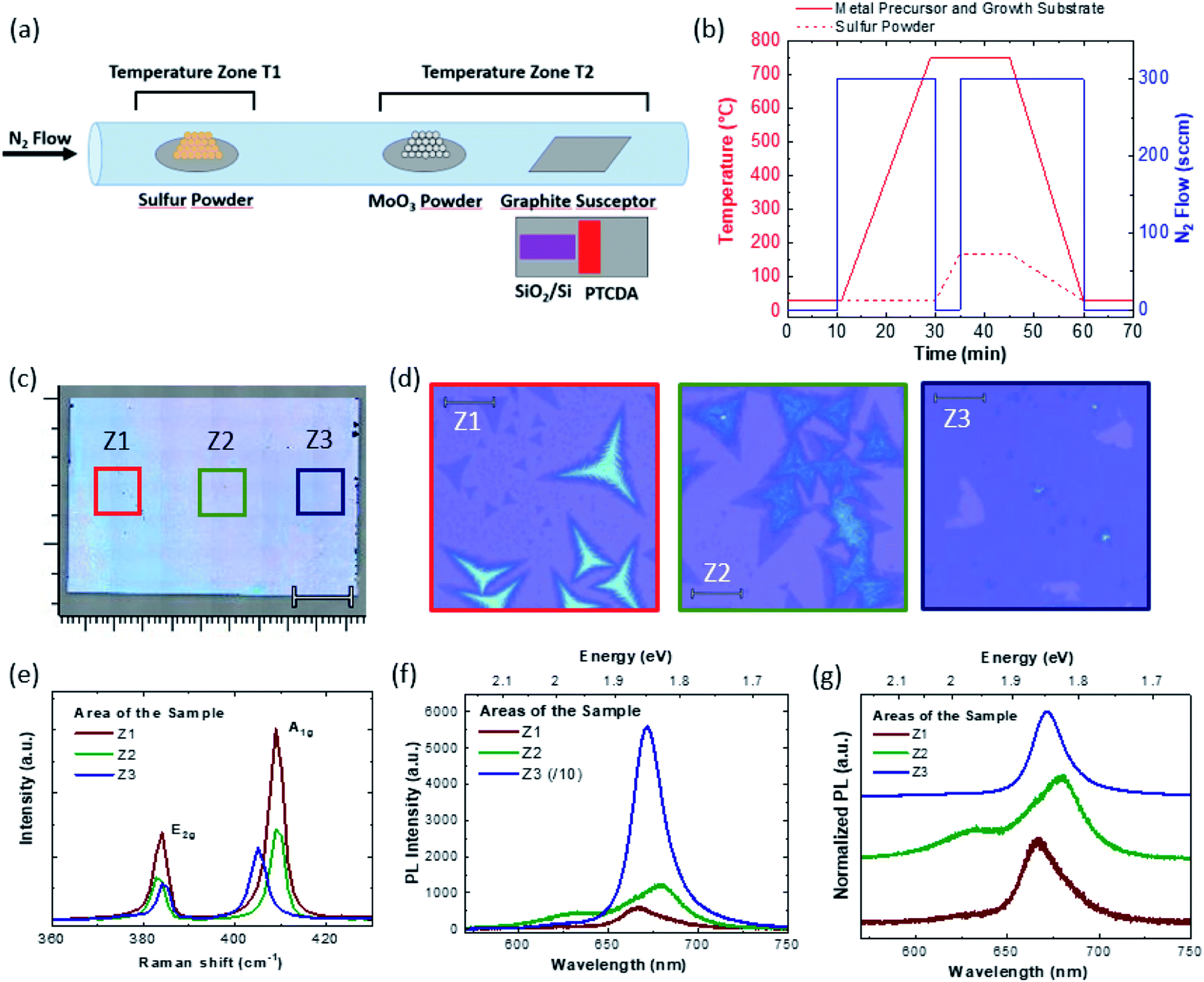 | ||
| Fig. 1 (a) Schematic illustration of the CVD reactor, with the configuration of the sulfur and Mo precursors and the disposition of the different substrates (b) Temperature (red lines) of the sulfur precursor (dashed line) and of the growth substrate (full line) and N2 carrier flow (blue line) during the growth process (c) optical image of the growth substrate, a different contrast induced by the presence of MoS2 is reported. The marker is 200 μm. (d) Optical images of the three areas named Z1 to Z3 highlighted by the colored squares in the panel (c). All the markers are 20 μm. The area Z1, the farthest from the PTCDA sacrificial substrate, shows the presence of MoS2 multi-layered dendritic structures and micrometric triangular monolayers, and the optical image of Z2 shows the presence of triangular crystals affected by overgrowth. Z3, the closest to the PTCDA substrate shows the presence of the MoS2 polycrystalline monolayer with high coverage, affected by a micrometric few-layer island, probably due to the seeding point of the crystal. (e) Large-area Raman spectroscopy spectra of the three areas in analysis. (f) Large area photoluminescence spectroscopy spectra of the same areas. The PL spectrum of Z3 is divided by 10 for the sake of clarity. (g) Normalized PL spectra. | ||
Fig. 1(b) summarizes the growth process, showing the precursor temperature and the N2 flow profile. In order to obtain a more controllable S flow during the MoS2 synthesis, we initially heated the substrate, the MoO3 powders at 750 °C under a flow of 300 sccm of N2, while keeping S at a low temperature (<70 °C). The downstream position of the PTCDA/Si substrate is chosen to maximize the gradient of the organic promoter: PTCDA decomposes during the heating ramp and diffuses upstream in the gas phase, depositing on SiO2. Due to the diffusion process, we expect a maximum PTCDA transfer to the growth substrate in the zone Z3, gradually decreasing to a minimum concentration in the zone Z1.37 After the growth, only carbon residues remain on the sacrificial substrate with PTCDA, as demonstrated by Raman analysis (Fig. S1 in the ESI†).
Once the set point temperature has been reached, the N2 flow was stopped and the S powder was separately heated to 170 °C, while maintaining a stagnant gas flow. This allowed limiting the S transport to the Mo powders and to the substrate during the temperature ramp; it was reported that this procedure prevents the uncontrollable reaction between the precursors during the pre-growth stage.43 The synthesis process lasts 10 minutes, and the system then cools down naturally to room temperature. In the optical image of the substrate after the growth process, a clear change in the optical contrast is evident from the closest to the farthermost areas with respect to the PTCDA substrate, red and blue squares respectively. The marker of the optical image is 200 μm. A false color image in Fig. 1(c), is reported in Fig. S2.† Optical images at higher magnification are reported in Fig. 1(d), where the different areas are labelled Z1 to Z3, with a decreasing distance from the PTCDA substrate. The high magnification optical images clarify the different optical contrasts of the whole sample image; Z1 presents large dendritic MoS2 multi-layer structures and micrometric triangular MoS2 flakes. In the Z2 area the lateral size of the MoS2 flakes increases up to 20 μm, although they are affected by dendritic overgrowth. In the Z3 area, the lateral size of the MoS2 flakes increases up to hundreds of micrometers, with few-layer terraces, most likely in the seeding points of the flakes. The monolayer coverage, observed by optical microscopy, varies between 77% and 93% in the Z3 area. The optical microscope observations are confirmed by large-area Raman and PL spectroscopies. Fig. 1(e) shows the comparison of the Raman spectra obtained in the different areas, as expected the separation of the E2g and A1g modes of MoS2, defined as Δ, changes in the different areas. In the case of Z1 and Z2, Δ is equal to 25 cm−1, the standard for bulk MoS2, and meanwhile Δ of Z3 is 21 cm−1, representative of the MoS2 bilayer. Raman analysis reveals no detectable amorphous carbon after the MoS2 growth process (Fig. S3†). Large-area spectroscopy spectra (Fig. 1(f)) show a peculiar behavior; Z3 shows the typical PL spectrum of the MoS2 monolayer, with an intense peak at 672 nm (1.85 eV) related to the A exciton,9 and meanwhile the other areas present weak PL emissions. The Z3 spectrum is divided by 10 for a direct comparison with the PL spectra of the other areas. In order to have a clear comparison of the PL peak position, the normalized PL spectra are reported in Fig. 1(g). Z2 shows an important red-shift of the A exciton emission with the PL peak at 680 nm (1.82 eV). Z2 also presents a tail toward the low wavelength side due to the B exciton of MoS2, peaked at 632 nm (1.96 eV). The Z3 PL spectrum presents a faint broad peak centered at 665 nm (1.86 eV), probably related to the presence of micrometric monolayer flakes. In Fig. S4† the result of a growth process without the PTCDA sacrificial substrate is reported in order to highlight the effect of the Mo/S ratio on these growth parameters.
Fig. 2 presents an accurate characterization of the morphological, optical and structural properties of the MoS2 dendritic multilayer structures, representative of Z1. Fig. 1(a) and (b) report the secondary electron and back-scattered electron images, respectively. The SE image shows a three branched architecture, with oblong structures originating from a central backbone. It is worth noting that the dendritic structure originates from a central triangular pyramid. Aberration corrected TEM analysis of different pyramids is reported in Fig. S5 of the ESI† file, and it shows that the 3D-pyramids are deeply affected by extended defects. The defects in these pyramids can lead to the development of dendritic multi-layer structures. The BSE image shows a peculiar contrast behavior; some areas have a dark contrast in comparison with the SiO2 substrate, while other areas present a bright contrast. This contrast inversion is probably due to the increase in the MoS2 work function with the increasing number of layers.44
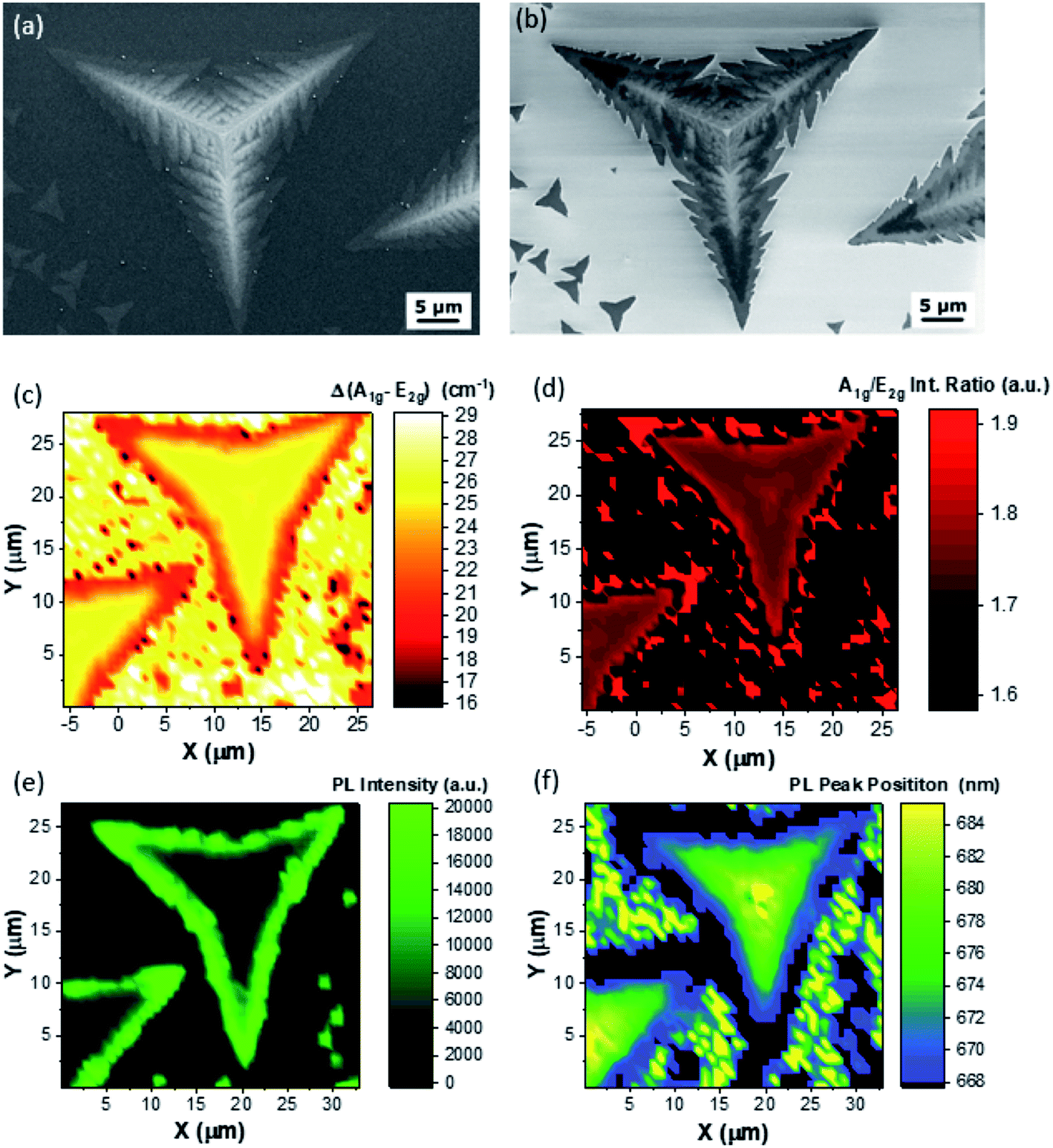 | ||
| Fig. 2 (a) SE micrograph of the dendritic structures representative of Z1, (b) BSE micrograph, (c) Raman map of the separation between the A1g and E2g modes, defined as Δ, (d) Raman map of the A1g and E2g mode intensity ratio, (e) PL intensity map of the MoS2 A exciton, and (f) PL peak position map of the MoS2 A exciton. | ||
The Raman maps of Δ and of the A1g/E2g intensity ratio are reported in Fig. 2(c) and (d), respectively. The Δ Raman map reveals that the dendritic structure presents an average Δ of 27 cm−1, indicating bulk MoS2, and meanwhile the edges have a Δ of 21 cm−1, indicative of MoS2 bilayers. The intensity ratio of the A1g and E2g is employed as a benchmark for the presence of defects, in particular sulfur vacancies, as previously reported.45,46 In this regard, the intensity ratio map shows that the center and the edges of the dendritic structure have a higher intensity ratio, an indication that these areas are more defective than the body of each branch. However, the intensity ratio map is also sensitive to the number of layers,47,48 and it can give similar information to the Δ Raman map. Indeed, the intensity ratio map, reported in Fig. 2(d) confirms the analysis of the Δ Raman map (Fig. 2(c)). PL mapping has been carried out to clarify the optical properties of the dendritic structures. The intensity and peak position of the MoS2 A exciton are presented in Fig. 2(e) and (f), respectively. As expected the central part of the dendritic structure presents a faint PL intensity of the MoS2 A exciton, due to the indirect band-gap of bulk MoS2. However, the PL intensity increases at the edge confirming the ML nature of the edges of the dendritic structure. It is worth noting that the PL peak position drastically red shifts from 668 nm, at the edges of the structure, up to 685 nm at the center of the dendritic structure. Fig. S6† presents the optical image of the structure reported in Fig. 2 and the representative PL spectra, extracted from the PL map.
The PL intensity and peak position maps perfectly overlap, demonstrating that the red-shift of the A exciton is related to the indirect-to-direct band gap transition of MoS2 in the monolayer form. The AFM analysis of the dendritic structure is reported in Fig. S7.†
A similar analysis has been carried out for the Z2 area. The SE image (Fig. 3(a)) reveals flakes with a lateral size varying from 30 to 50 μm. The dendritic overgrowth occurs close to the center of the flakes, probably starting at the seeding point of the flake itself. The BSE image (Fig. 3(b)) shows the presence of few-layer terraces (area with a brighter contrast). It is possible to convey that these terraces are few-layers by comparing the SE and the BSE images; indeed the SE image does not show any morphological contrast and meanwhile the BSE image presents a clear contrast. Raman mapping permits the clarification of the number of layers of these particular few-layer terraces. Fig. 3(c) reports the Δ map, showing that the flakes are mainly monolayer (Δ = 19 cm−1) and the dendritic overgrowth is bulk with a value ranging from 23 cm−1 to 26 cm−1. However, the Δ map reveals the presence of bilayer terraces, similar to that reported by the BSE imaging with Δ equal to 21 cm−1, representative of bilayer MoS2. Furthermore, all the few-layer areas, both the bilayer terraces and the dendritic overgrowth areas, present a lower intensity ratio of the Raman modes (Fig. 3(d)): this is a clear indication that the few-layer area is less defective than the MLs. Even in this case the intensity ratio map confirms the analysis of the Δ Raman maps. In addition, the bilayer nature of such terraces is confirmed by PL intensity mapping (Fig. 3(e)): as a matter of fact, the terraces present a slightly local decrease in the PL intensity and the decrease is more enhanced in the dendritic overgrowth areas. In the case of the A exciton peak position map, the peak varies from 683 nm (1.815 eV) to 685 nm (1.81 eV) in the ML area. In the bilayer and dendritic overgrowth area the PL peak is at around 682 nm (1.82 eV). This is in agreement with the large area PL analysis presented in Fig. 1(g). The optical image of the structure reported in Fig. 3 and the representative PL spectra are shown in Fig. S8.† The AFM analysis of the overgrowth affected flake is reported in Fig. S9.†
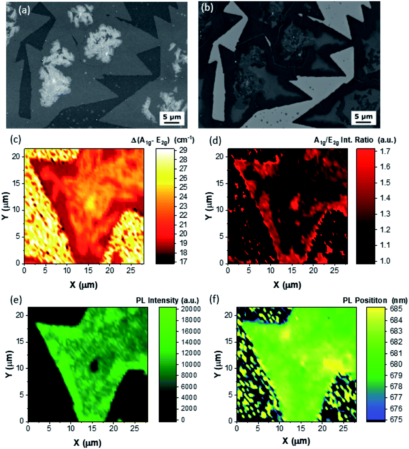 | ||
| Fig. 3 (a) SE micrograph of the MoS2 flakes affected by dendritic overgrowth, representative of Z2, (b) BSE micrograph, (c) Raman map of the separation between the A1g and E2g modes, defined as Δ, (d) Raman map of the A1g and E2g mode intensity ratio, (e) PL intensity map of the MoS2 A exciton, and (f) PL peak position map of the MoS2 A exciton. | ||
In Fig. 4 we present the morphological, structural and optical properties of large-area polycrystalline monolayer MoS2, representative of Z3. The SE image reveals that the lateral size of the MoS2 is difficult to evaluate due to the coalescence to a polycrystalline quasi-continuous film. It is worth noting that the SE analysis reveals the presence of bright and dark round features probably related to residuals of organic promoters33,38 and craters.33 The comparison with the BSE images (Fig. 4(b)) shows the presence of few-layer terraces, similarl to the overgrowth affected flakes reported in Fig. 3, and of grain-boundaries, demonstrating the polycrystalline nature of the MoS2 film. The Δ Raman map confirms the monolayer nature of the edges of the flakes with an average Δ equal to 18.5 cm−1; meanwhile the central part of the flake is composed of bilayer terraces, with an average Δ equal to 20 cm−1. The intensity ratio map (Fig. 4(d)) reveals a faint contrast demonstrating a comparable concentration of defects of the monolayer and bilayer MoS2. The comparison between the Δ Raman map and the intensity ratio shows a slightly different spatial localization, revealing that probably, in this case, the different concentrations of point defects is more effective than the number of layers. The PL intensity map of the A exciton of MoS2 (Fig. 4(e)) shows peculiar homogeneity; however in the case of the polycrystalline MoS2 the PL peak position of the MoS2 A exciton shows that the exciton in the bilayer terraces (685 nm) is red-shifted by 5 nm in comparison with the ML areas (680 nm). It is worth noting that the edges and the grain boundaries present a blue shift, revealing the PL peak position set at 678 nm. Some PL spectra, extracted from the map, are shown in Fig. S10.† The AFM analysis of the overgrowth affected flake is reported in Fig. S11.† In order to evaluate the crystalline quality of the MoS2 film aberration corrected Scanning Transmission Electron Microscopy (STEM) has been carried out (Fig. 5). A similar Raman and PL analyses are reported in Fig. S12† for another area of the polycrystalline MoS2.
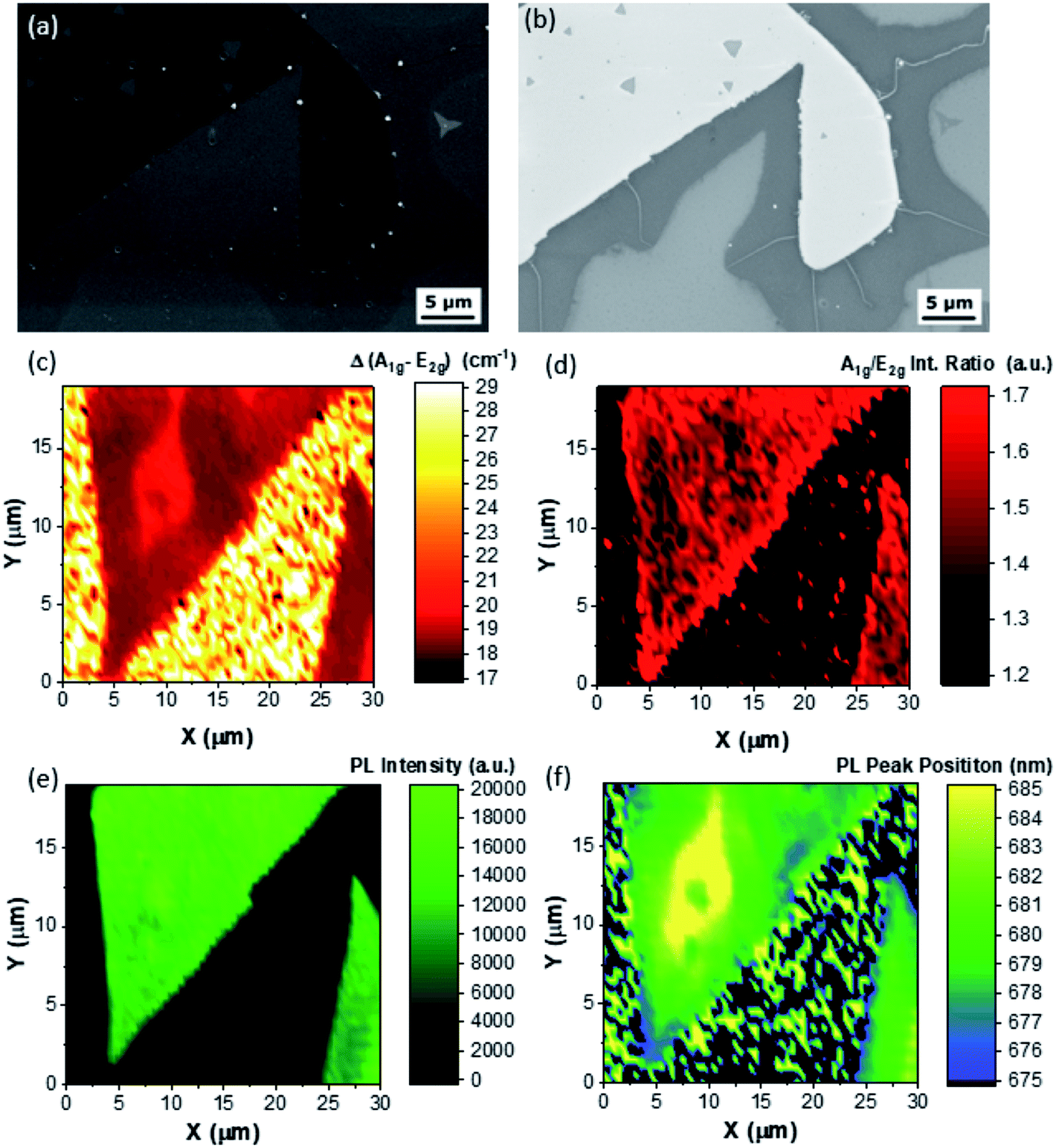 | ||
| Fig. 4 (a) SE micrograph of large polycrystalline MoS2, representative of Z3, (b) BSE micrograph, (c) Raman map of the separation between the A1g and E2g modes, defined as Δ, (d) Raman map of the A1g and E2g mode intensity ratio, (e) PL intensity map of the MoS2 A exciton, and (f) PL peak position map of the MoS2 A exciton. | ||
 | ||
| Fig. 5 Aberration corrected TEM analysis results of the flake transferred from Z3, (a) interface area between a MoS2 monolayer and bilayer, (b) and (c) bilayer and monolayer atomically resolved TEM image, respectively. | ||
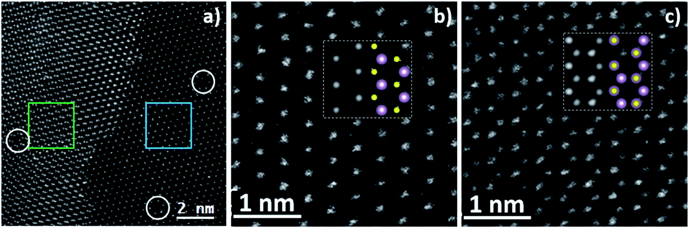
The MoS2 flake has been transferred (see Methods) from the Z3 area of the sample where mainly mono and bilayer MoS2 can be found, and in particular we focused our attention on the interface between the monolayer and bilayer highlighted in Fig. 4.
Two very high magnification atomic resolution images have been taken (reported in Fig. 5(b) and (c)) in the blue and green squared region located in the monolayer and bilayer respectively in order to confirm the crystalline quality of the sample and, at the same time, to count the number of layers. This last task can be easily achieved by analysing the atomic patterns. As a matter of fact, in the single layer MoS2 the Mo and S atoms are alternately located at the six corners of an hexagon49 and they show a different contrast in the image in Fig. 5(b), see ESI Fig. S13.†
On the other hand, in the bilayer MoS2, the second layer is rotated by 60° with respect to the first one, resulting in the superposition of the two atomic species. Consequently, all the atomic columns will contain the same number of atoms showing the same contrast in the HAADF image reported in image 5c.
As a further confirmation, we performed multislice STEM simulations,50 finding a perfect match between the experimental and the simulated images, which are reported as insets along with the crystal models.
Beside these extra layers, the MoS2 flakes are defect free and they have very high crystallinity as apparent from the images of the atomic lattice. Nevertheless, some vacancies can be observed in Fig. 5(a) highlighted by white circles; however the formation of electron beam induced vacancies is a well reported phenomenon and51 therefore these defects cannot be univocally ascribed to growth.52
Fig. 6 illustrates the MoS2 growth dynamics in the presence of the two opposite flows, the flow of the sulfur and molybdenum precursors (MoO3) and the backflow of PTCDA. The latter results in a gradient of the growth-promoter on the SiO2 substrate, causing a change in the MoS2 structure morphology and lateral size along the length of the growth substrate. We expect a maximum promoter concentration in the zone Z3 and a minimum concentration in Z1. First, the size of the monolayer triangular flake increases laterally from few micrometers to several tens of micrometers, getting close to the sacrificial PTCDA substrate. The increase of the size of triangular monolayer crystals is the direct effect of the PTCDA, which acts as a growth promoter favoring the lateral growth of the flakes. In fact, as previously reported, by employing PTCDA it is possible to achieve the complete coverage of the growth substrate.37 In addition, the presence of dendritic structures decreases. Albeit the growth of dendritic structures of transition metal dichalcogenides previously reported, the origin of this particular effect is not completely clarified. The Kinetic Monte Carlo (KMC) method was used to simulate the growth behavior during van der Waals epitaxy growth of WSe2 and other atomically thin TMD films.53,54 The shape transition from triangular crystals to fractal and dendritic structures corresponds to the change in the growth parameters.55,56 In particular, the simulation shows that one important parameter in order to achieve dendritic and fractal structures is the ratio of the chalcogen and metal flow53 as experimentally verified in recent studies.55,57,58
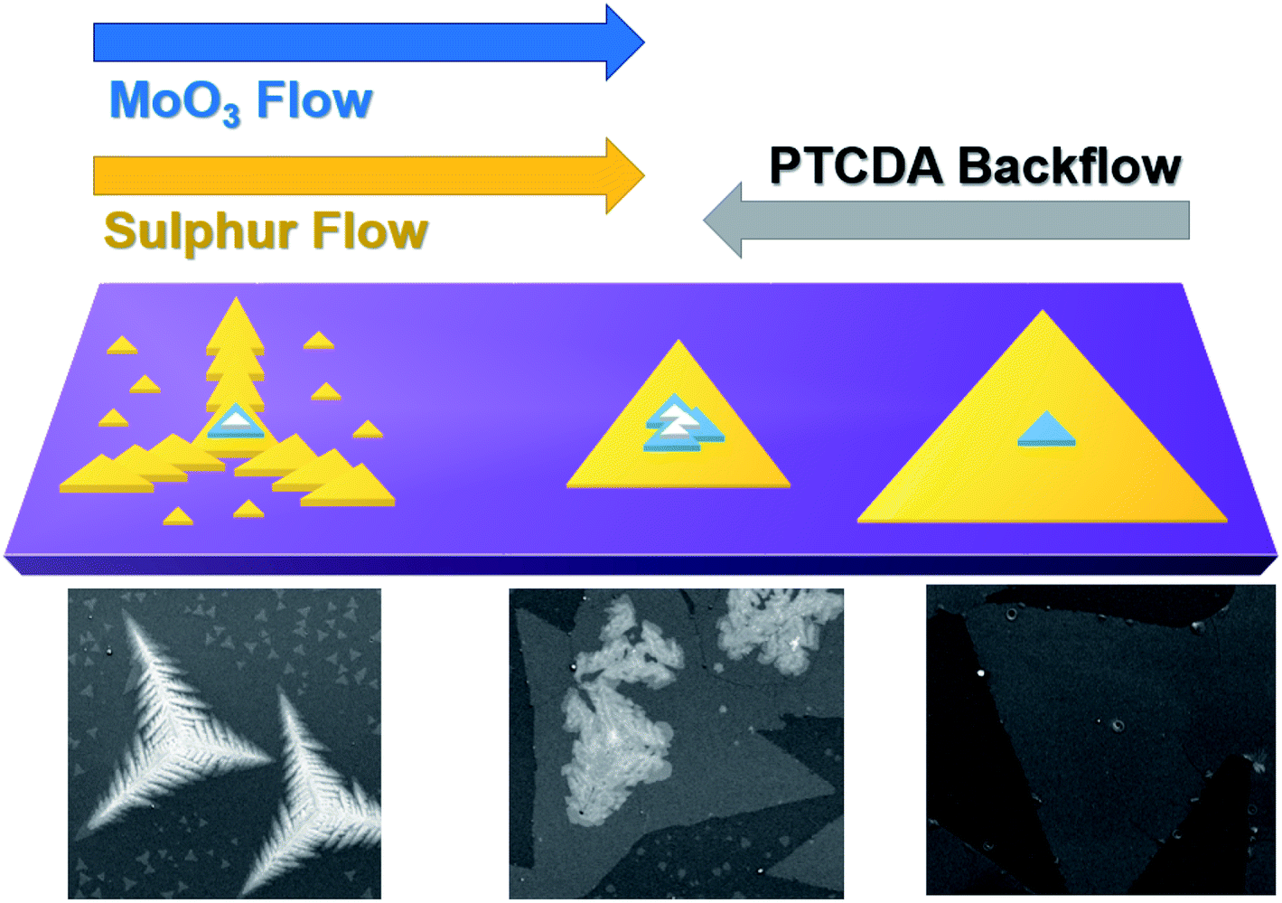 | ||
| Fig. 6 Schematic illustration of the growth dynamics of MoS2 considering the gradient of the organic promoter (PTCDA) with representative SEM images of the different areas. | ||
Another possible origin of the dendritic and fractal structures is their formation at the initial stage of the growth of a high-quality TMD triangular monolayer. In fact, the high growth rate is predicted to occur through a two-step process: after the formation of fractal/dendritic structures, they can eventually evolve into highly crystalline triangular structures. This possible origin was experimentally addressed in the case of growth of WS2 triangular flakes on SiO2/Si substrates.59 One important aspect of the dendritic TMD structure is the hierarchy level. A high level of hierarchy is normally reported in the case of six branched structures due to the presence of twin boundaries.57,58
Most of the studies presenting dendritic structures do not employ a growth promoter except for the work of J. Wang et al.58 in which the authors employed tape glue residuals to promote CVD growth. It is noticeable that the dendritic structure morphologies depend on which tape was used in the growth process.
It is worth noting that in this work we never obtain dendritic structures with a high hierarchy level. We report three branched structures, however, in our case the central part of the dendritic structure is multi-layer, as demonstrated by Raman and PL mappings. We assume that the dendritic structures probably originate from three-dimensional defective pyramids (Fig. S5†) found at the center of the dendritic structures, as suggested by the multi-layer central part of the structure (Fig. 2 and S7†). The crystalline disorder due to the extended defects in the central pyramid can cause the growth of the dendritic structures. The synthesis of the three dimensional pyramidal seeds can be due to inhomogeneity of the PTCDA growth promoter on SiO2 boosting three dimensional growth. These effects are supported by a recent study,60 where by utilizing a porphyrin based promoter (5,10,15,20-tetrakis(4-hydroxyphenyl)-21H, 23H-porphyrin) large-scale vertically oriented MoS2 nanoflakes were obtained. In particular, the thickness of the promoter layer was important to achieve large scale homogeneity.
Conclusions
In conclusion we clarify the effect of gradient of an organic promoter on the growth dynamics of molybdenum disulphide. We employ a perylene-based growth promoter (PTCDA) that sublimates during the heating ramp and diffuses upstream in the gas phase. A substrate covered with the promoter is placed downstream with respect to the growth substrate; the promoter is transferred to the growth substrate by upstream flow diffusion, thus creating a gradient of its distribution. The farthest zone from the sacrificial promoter substrate presents micrometric triangular monolayers and dendritic multi-layer MoS2 branched structures. This growth dynamics demonstrates that a low amount of organic promoter leads to reduced lateral growth and boosting of the vertical growth. We suppose that the dendritic structures originate from three-dimensional defective pyramids found at the center of these structures. In the zone closest to the promoter substrate, a quasi-continuous MoS2 polycrystalline film has been found, demonstrating that a high quantity of growth promoter enhances the lateral growth, suppressing the vertical one. However, the presence of bilayer terraces is reported. The transition zone presents monolayer crystals with an average lateral size of 50 micrometers affected by multilayer dendritic overgrowth at the flake center, supporting the direct connection between the flow gradient and the MoS2 growth dynamics.Conflicts of interest
There are no conflicts to declare.Acknowledgements
F. F. wants to thank Dr Pasqualantonio Pingue for the help in the analysis of the AFM images. Dr Corneliu Ghica (National Institute of Materials Physics, Magurele, Ro) is acknowledged for the help in the TEM analysis.References
- C. Cong, J. Shang, Y. Wang and T. Yu, Optical Properties of 2D Semiconductor WS2, Adv. Opt. Mater., 2018, 6(1), 1700767, DOI:10.1002/adom.201700767.
- S. Manzeli, D. Ovchinnikov, D. Pasquier, O. V. Yazyev and A. Kis, 2D Transition Metal Dichalcogenides, in Nature Reviews Materials, Nature Publishing Group, 2017. DOI:10.1038/natrevmats.2017.33.
- Q. H. Wang, K. Kalantar-Zadeh, A. Kis, J. N. Coleman and M. S. Strano, Electronics and Optoelectronics of Two-Dimensional Transition Metal Dichalcogenides, Nat. Nanotechnol., 2012, 7(11), 699–712, DOI:10.1038/nnano.2012.193.
- G. Fiori, F. Bonaccorso, G. Iannaccone, T. Palacios, D. Neumaier, A. Seabaugh, S. K. Banerjee and L. Colombo, Electronics Based on Two-Dimensional Materials, Nat. Nanotechnol., 2014, 768–779, DOI:10.1038/nnano.2014.207.
- M. Amani, D. H. Lien, D. Kiriya, J. Xiao, A. Azcatl, J. Noh, S. R. Madhvapathy, R. Addou, K. C. Santosh and M. Dubey, et al. Near-Unity Photoluminescence Quantum Yield in MoS2, Science, 2015, 350(6264), 1065–1068, DOI:10.1126/science.aad2114.
- C.-H. Yeh, Z.-Y. Liang, Y.-C. Lin, H.-C. Chen, T. Fan, C.-H. Ma, Y.-H. Chu, K. Suenaga and P.-W. Chiu, Graphene–Transition Metal Dichalcogenide Heterojunctions for Scalable and Low-Power Complementary Integrated Circuits, ACS Nano, 2020, 14(1), 985–992, DOI:10.1021/acsnano.9b08288.
- H. Wang, L. Yu, Y. H. Lee, Y. Shi, A. Hsu, M. L. Chin, L. J. Li, M. Dubey, J. Kong and T. Palacios, Integrated Circuits Based on Bilayer MoS2 Transistors, Nano Lett., 2012, 12(9), 4674–4680, DOI:10.1021/nl302015v.
- B. Radisavljevic, M. B. Whitwick and A. Kis, Integrated Circuits and Logic Operations Based on Single-Layer MoS2, ACS Nano, 2011, 5(12), 9934–9938, DOI:10.1021/nn203715c.
- A. Splendiani, L. Sun, Y. Zhang, T. Li, J. Kim, C. Y. Chim, G. Galli and F. Wang, Emerging Photoluminescence in Monolayer MoS2, Nano Lett., 2010, 10(4), 1271–1275, DOI:10.1021/nl903868w.
- K. F. Mak, C. Lee, J. Hone, J. Shan and T. F. Heinz, Atomically Thin MoS2: A New Direct-Gap Semiconductor, Phys. Rev. Lett., 2010, 105(13), 136805, DOI:10.1103/PhysRevLett.105.136805.
- J. Gu, B. Chakraborty, M. Khatoniar and V. M. Menon, A Room-Temperature Polariton Light-Emitting Diode Based on Monolayer WS2, Nat. Nanotechnol., 2019, 1024–1028, DOI:10.1038/s41565-019-0543-6.
- S. Jo, N. Ubrig, H. Berger, A. B. Kuzmenko and A. F. Morpurgo, Mono- and Bilayer WS2 Light-Emitting Transistors, Nano Lett., 2014, 14(4), 2019–2025, DOI:10.1021/nl500171v.
- Y. Ye, Z. J. Wong, X. Lu, X. Ni, H. Zhu, X. Chen, Y. Wang and X. Zhang, Monolayer Excitonic Laser, Nat. Photonics, 2015, 9(11), 733–737, DOI:10.1038/nphoton.2015.197.
- D. Unuchek, A. Ciarrocchi, A. Avsar, K. Watanabe, T. Taniguchi and A. Kis, Room-Temperature Electrical Control of Exciton Flux in a van Der Waals Heterostructure, Nature, 2018, 340–344, DOI:10.1038/s41586-018-0357-y.
- Z. Sun, A. Martinez and F. Wang, Optical Modulators with 2D Layered Materials, Nat. Photonics, 2016, 227–238, DOI:10.1038/nphoton.2016.15.
- K. F. Mak and J. Shan, Photonics and Optoelectronics of 2D Semiconductor Transition Metal Dichalcogenides, Nat. Photonics, 2016, 216–226, DOI:10.1038/nphoton.2015.282.
- T. Cao, G. Wang, W. Han, H. Ye, C. Zhu, J. Shi, Q. Niu, P. Tan, E. Wang and B. Liu, et al. Valley-Selective Circular Dichroism of Monolayer Molybdenum Disulphide, Nat. Commun., 2012, 3, 887, DOI:10.1038/ncomms1882.
- K. F. Mak, K. L. McGill, J. Park and P. L. McEuen, The Valley Hall Effect in MoS2 Transistors, Science, 2014, 344(6191), 1489–1492, DOI:10.1126/science.1250140.
- D. Unuchek, A. Ciarrocchi, A. Avsar, Z. Sun, K. Watanabe, T. Taniguchi and A. Kis, Valley-Polarized Exciton Currents in a van Der Waals Heterostructure, Nat. Nanotechnol., 2019, 1104–1109, DOI:10.1038/s41565-019-0559-y.
- D. Shin, H. Hübener, U. De Giovannini, H. Jin, A. Rubio and N. Park, Phonon-Driven Spin-Floquet Magneto-Valleytronics in MoS2, Nat. Commun., 2018, 9(1), 638, DOI:10.1038/s41467-018-02918-5.
- Y. K. Luo, J. Xu, T. Zhu, G. Wu, E. J. McCormick, W. Zhan, M. R. Neupane and R. K. Kawakami, Opto-Valleytronic Spin Injection in Monolayer MoS2/Few-Layer Graphene Hybrid Spin Valves, Nano Lett., 2017, 17(6), 3877–3883, DOI:10.1021/acs.nanolett.7b01393.
- M. Bosi, Growth and Synthesis of Mono and Few-Layers Transition Metal Dichalcogenides by Vapour Techniques: A Review, RSC Adv., 2015, 5(92), 75500–75518, 10.1039/c5ra09356b.
- D. Dumcenco, D. Ovchinnikov, K. Marinov, P. Lazić, M. Gibertini, N. Marzari, O. L. Sanchez, Y. C. Kung, D. Krasnozhon and M. W. Chen, et al. Large-Area Epitaxial Monolayer MoS2, ACS Nano, 2015, 9(4), 4611–4620, DOI:10.1021/acsnano.5b01281.
- Y. Zhan, Z. Liu, S. Najmaei, P. M. Ajayan and J. Lou, Large-Area Vapor-Phase Growth and Characterization of MoS 2 Atomic Layers on a SiO2 Substrate, Small, 2012, 8(7), 966–971, DOI:10.1002/smll.201102654.
- Y.-H. Lee, X.-Q. Zhang, W. Zhang, M.-T. Chang, C.-T. Lin, K.-D. Chang, Y.-C. Yu, J. T.-W. Wang, C.-S. Chang and L.-J. Li, et al. Synthesis of Large-Area MoS 2 Atomic Layers with Chemical Vapor Deposition, Adv. Mater., 2012, 24(17), 2320–2325, DOI:10.1002/adma.201104798.
- K. K. Liu, W. Zhang, Y. H. Lee, Y. C. Lin, M. T. Chang, C. Y. Su, C. S. Chang, H. Li, Y. Shi and H. Zhang, et al. Growth of Large-Area and Highly Crystalline MoS 2 Thin Layers on Insulating Substrates, Nano Lett., 2012, 12(3), 1538–1544, DOI:10.1021/nl2043612.
- F. Tumino, C. S. Casari, M. Passoni, V. Russo and A. Li Bassi, Pulsed Laser Deposition of Single-Layer MoS2 on Au(111): From Nanosized Crystals to Large-Area Films, Nanoscale Adv., 2019, 1(2), 643–655, 10.1039/c8na00126j.
- T. Schram, Q. Smets, B. Groven, M. H. Heyne, E. Kunnen, A. Thiam, K. Devriendt, A. Delabie, D. Lin, and M. Lux, et al. WS2 Transistors on 300 Mm Wafers with BEOL Compatibility, in European Solid-State Device Research Conference, Editions Frontieres, 2017, pp. 212–215. DOI:10.1109/ESSDERC.2017.8066629.
- A. Kozhakhmetov, J. Nasr, F. Zhang, K. Xu, N. Briggs, R. Addou, R. M. Wallace, S. K. Fullerton-Shirey, M. Terrones and S. Das, et al. Scalable BEOL Compatible Two-Dimensional Tungsten Diselenide, 2D Mater, 2019 DOI:10.1088/2053-1583/ab5ad1.
- S. Cwik, D. Mitoraj, O. Mendoza Reyes, D. Rogalla, D. Peeters, J. Kim, H. M. Schütz, C. Bock, R. Beranek and A. Devi, Direct Growth of MoS 2 and WS 2 Layers by Metal Organic Chemical Vapor Deposition, Adv. Mater. Interfaces, 2018, 5(16), 1800140, DOI:10.1002/admi.201800140.
- D. Andrzejewski, H. Myja, M. Heuken, A. Grundmann, H. Kalisch, A. Vescan, T. Kümmell and G. Bacher, Scalable Large-Area p–i–n Light-Emitting Diodes Based on WS 2 Monolayers Grown via MOCVD, ACS Photonics, 2019, 6(8), 1832–1839, DOI:10.1021/acsphotonics.9b00311.
- H. Kim, D. Ovchinnikov, D. Deiana, D. Unuchek and A. Kis, Suppressing Nucleation in Metal–Organic Chemical Vapor Deposition of MoS 2 Monolayers by Alkali Metal Halides, Nano Lett., 2017, 17(8), 5056–5063, DOI:10.1021/acs.nanolett.7b02311.
- H. Kim, G. H. Han, S. J. Yun, J. Zhao, D. H. Keum, H. Y. Jeong, T. H. Ly, Y. Jin, J. H. Park and B. H. Moon, et al. Role of Alkali Metal Promoter in Enhancing Lateral Growth of Monolayer Transition Metal Dichalcogenides, Nanotechnology, 2017, 28(36), 36LT01, DOI:10.1088/1361-6528/aa7e5e.
- H. Cun, M. Macha, H. K. Kim, K. Liu, Y. Zhao, T. LaGrange, A. Kis and A. Radenovic, Wafer-Scale MOCVD Growth of Monolayer MoS2 on Sapphire and SiO2, Nano Res., 2019, 12(10), 2646–2652, DOI:10.1007/s12274-019-2502-9.
- S. J. Kim, M. A. Kang, S. H. Kim, Y. Lee, W. Song, S. Myung, S. S. Lee, J. Lim and K. S. An, Large-Scale Growth and Simultaneous Doping of Molybdenum Disulfide Nanosheets, Sci. Rep., 2016, 6, 24054, DOI:10.1038/srep24054.
- H. F. Liu, S. L. Wong and D. Z. Chi, CVD Growth of MoS 2 -Based Two-Dimensional Materials, Chem. Vap. Deposition, 2015, 21(10-11-12), 241–259, DOI:10.1002/cvde.201500060.
- X. Ling, Y. H. Lee, Y. Lin, W. Fang, L. Yu, M. S. Dresselhaus and J. Kong, Role of the Seeding Promoter in MoS2 Growth by Chemical Vapor Deposition, Nano Lett., 2014, 14(2), 464–472, DOI:10.1021/nl4033704.
- P. Yang, A.-G. Yang, L. Chen, J. Chen, Y. Zhang, H. Wang, L. Hu, R.-J. Zhang, R. Liu and X.-P. Qu, et al. Influence of Seeding Promoters on the Properties of CVD Grown Monolayer Molybdenum Disulfide, Nano Res., 2019, 12, 823–827, DOI:10.1007/s12274-019-2294-y.
- X. Q. Zhang, C. H. Lin, Y. W. Tseng, K. H. Huang and Y. H. Lee, Synthesis of Lateral Heterostructures of Semiconducting Atomic Layers, Nano Lett., 2015, 15(1), 410–415, DOI:10.1021/nl503744f.
- P. Yang, A. G. Yang, L. Chen, J. Chen, Y. Zhang, H. Wang, L. Hu, R. J. Zhang, R. Liu and X. P. Qu, et al. Influence of Seeding Promoters on the Properties of CVD Grown Monolayer Molybdenum Disulfide, Nano Res., 2019, 12(4), 823–827, DOI:10.1007/s12274-019-2294-y.
- D. Dumcenco, D. Ovchinnikov, O. L. Sanchez, P. Gillet, D. T. L. Alexander, S. Lazar, A. Radenovic and A. Kis, Large-Area MoS2 Grown Using H 2 S as the Sulphur Source, 2D Mater, 2015, 2(4), 044005, DOI:10.1088/2053-1583/2/4/044005.
- S. Wang, G. D. Lee, S. Lee, E. Yoon and J. H. Warner, Detailed Atomic Reconstruction of Extended Line Defects in Monolayer MoS2, ACS Nano, 2016, 10(5), 5419–5430, DOI:10.1021/acsnano.6b01673.
- H. Liu, Y. Zhu, Q. Meng, X. Lu, S. Kong, Z. Huang, P. Jiang and X. Bao, Role of the Carrier Gas Flow Rate in Monolayer MoS2 Growth by Modified Chemical Vapor Deposition, Nano Res., 2017, 10(2), 643–651, DOI:10.1007/s12274-016-1323-3.
- M. Tamulewicz, J. Kutrowska-Girzycka, K. Gajewski, J. Serafińczuk, A. Sierakowski, J. Jadczak, L. Bryja and T. P. Gotszalk, Layer Number Dependence of the Work Function and Optical Properties of Single and Few Layers MoS2: Effect of Substrate, Nanotechnology, 2019, 30(24), 245708, DOI:10.1088/1361-6528/ab0caf.
- F. Fabbri, E. Rotunno, E. Cinquanta, D. Campi, E. Bonnini, D. Kaplan, L. Lazzarini, M. Bernasconi, C. Ferrari and M. Longo, et al. Novel Near-Infrared Emission from Crystal Defects in MoS 2 Multilayer Flakes, Nat. Commun., 2016, 7, 13044, DOI:10.1038/ncomms13044.
- W. M. Parkin, A. Balan, L. Liang, P. M. Das, M. Lamparski, C. H. Naylor, J. A. Rodríguez-Manzo, A. T. C. Johnson, V. Meunier and M. Drndić, Raman Shifts in Electron-Irradiated Monolayer MoS2, ACS Nano, 2016, 10(4), 4134–4142, DOI:10.1021/acsnano.5b07388.
- L. Liang and V. Meunier, First-Principles Raman Spectra of MoS2, WS2 and Their Heterostructures, Nanoscale, 2014, 6(10), 5394–5401, 10.1039/c3nr06906k.
- B. Chakraborty, H. S. S. R. Matte, A. K. Sood and C. N. R. Rao, Layer-Dependent Resonant Raman Scattering of a Few Layer MoS 2, J. Raman Spectrosc., 2013, 44(1), 92–96, DOI:10.1002/jrs.4147.
- A. Kuc, Low-Dimensional Transition-Metal Dichalcogenides, Chem. Modell., 2015, 11, 1–29, 10.1039/9781782620112-00001.
- V. Grillo and E. Rotunno, STEM CELL: A Software Tool for Electron Microscopy: Part I-Simulations, Ultramicroscopy, 2013, 125, 97–111, DOI:10.1016/j.ultramic.2012.10.016.
- E. Rotunno, F. Fabbri, E. Cinquanta, D. Kaplan, M. Longo, L. Lazzarini, A. Molle, V. Swaminathan and G. Salviati, Structural, Optical and Compositional Stability of MoS2 Multi-Layer Flakes under High Dose Electron Beam Irradiation, 2D Mater., 2016, 3(2), 025024, DOI:10.1088/2053-1583/3/2/025024.
- J. Hong, Z. Hu, M. Probert, K. Li, D. Lv, X. Yang, L. Gu, N. Mao, Q. Feng and L. Xie, et al. Exploring Atomic Defects in Molybdenum Disulphide Monolayers, Nat. Commun., 2015, 6, 6293, DOI:10.1038/ncomms7293.
- Y. Nie, C. Liang, P. R. Cha, L. Colombo, R. M. Wallace and K. Cho, A Kinetic Monte Carlo Simulation Method of van Der Waals Epitaxy for Atomistic Nucleation-Growth Processes of Transition Metal Dichalcogenides, Sci. Rep., 2017, 7(1), 2977, DOI:10.1038/s41598-017-02919-2.
- Y. Nie, C. Liang, K. Zhang, R. Zhao, S. M. Eichfeld, P. R. Cha, L. Colombo, J. A. Robinson, R. M. Wallace and K. Cho, First Principles Kinetic Monte Carlo Study on the Growth Patterns of WSe2 Monolayer, 2D Mater., 2016, 3(2), 025029, DOI:10.1088/2053-1583/3/2/025029.
- A. Govind Rajan, J. H. Warner, D. Blankschtein and M. S. Strano, Generalized Mechanistic Model for the Chemical Vapor Deposition of 2D Transition Metal Dichalcogenide Monolayers, ACS Nano, 2016, 10(4), 4330–4344, DOI:10.1021/acsnano.5b07916.
- S. Wang, Y. Rong, Y. Fan, M. Pacios, H. Bhaskaran, K. He and J. H. Warner, Shape Evolution of Monolayer MoS2 Crystals Grown by Chemical Vapor Deposition, Chem. Mater., 2014, 26(22), 6371–6379, DOI:10.1021/cm5025662.
- W. Xu, S. Li, S. Zhou, J. K. Lee, S. Wang, S. G. Sarwat, X. Wang, H. Bhaskaran, M. Pasta and J. H. Warner, Large Dendritic Monolayer MoS 2 Grown by Atmospheric Pressure Chemical Vapor Deposition for Electrocatalysis, ACS Appl. Mater. Interfaces, 2018, 10(5), 4630–4639, DOI:10.1021/acsami.7b14861.
- J. Wang, X. Cai, R. Shi, Z. Wu, W. Wang, G. Long, Y. Tang, N. Cai, W. Ouyang and P. Geng, et al. Twin Defect Derived Growth of Atomically Thin MoS2 Dendrites, ACS Nano, 2018, 12(1), 635–643, DOI:10.1021/acsnano.7b07693.
- C. Cong, J. Shang, X. Wu, B. Cao, N. Peimyoo, C. Qiu, L. Sun and T. Yu, Synthesis and Optical Properties of Large-Area Single-Crystalline 2D Semiconductor WS 2 Monolayer from Chemical Vapor Deposition, Adv. Opt. Mater., 2014, 2(2), 131–136, DOI:10.1002/adom.201300428.
- M. A. Kang, S. K. Kim, J. K. Han, S. J. Kim, S. J. Chang, C. Y. Park, S. Myung, W. Song, S. S. Lee and J. Lim, et al. Large Scale Growth of Vertically Standing MoS 2 Flakes on 2D Nanosheet Using Organic Promoter, 2D Mater., 2017, 4(2), 025042, DOI:10.1088/2053-1583/aa6049.
Footnote |
| † Electronic supplementary information (ESI) available. See DOI: 10.1039/d0na00147c |
| This journal is © The Royal Society of Chemistry 2020 |