
 Open Access Article
 This Open Access Article is licensed under a Creative Commons Attribution-Non Commercial 3.0 Unported Licence
Three-dimensional hierarchical semi-polar GaN/InGaN MQW coaxial nanowires on a patterned Si nanowire template†
Muhammad Ali
Johar‡
 a,
Taeyun
Kim‡
a,
Hyun-Gyu
Song
b,
Aadil
Waseem
a,
Jin-Ho
Kang
ac,
Mostafa Afifi
Hassan
a,
Indrajit V.
Bagal
a,
Yong-Hoon
Cho
b and
Sang-Wan
Ryu
*a
a,
Taeyun
Kim‡
a,
Hyun-Gyu
Song
b,
Aadil
Waseem
a,
Jin-Ho
Kang
ac,
Mostafa Afifi
Hassan
a,
Indrajit V.
Bagal
a,
Yong-Hoon
Cho
b and
Sang-Wan
Ryu
*a
aDepartment of Physics, Chonnam National University, Gwangju 61186, Republic of Korea. E-mail: sangwan@chonnam.ac.kr
bDepartment of Physics, Korea Advanced Institute of Science and Technology, Daejeon 34141, Republic of Korea
cDepartment of Electrical Engineering, Yale University, New Haven, CT, USA
First published on 12th March 2020
Abstract
We have demonstrated for the first time the hybrid development of next-generation 3-D hierarchical GaN/InGaN multiple-quantum-well nanowires on a patterned Si nanowire-template. The patterned Si nanowire-template is fabricated using metal-assisted chemical-etching, and the conformal growth of the GaN/InGaN multiple-quantum-well (MQW) coaxial nanowires is conducted using metal–organic-chemical-vapor-deposition by the two-step growth approach of vapor–liquid–solid for the GaN core and vapor–solid for the GaN/InGaN MQW shells. The growth directions of the GaN nanowires are confirmed by transmission electron microscopy and selected area electron diffraction patterns. The emission of the GaN/InGaN MQW nanowire is tuned from 440 nm to 505 nm by increasing the InGaN quantum-well thickness. The carrier dynamics were evaluated by performing temperature-dependent time-resolved photoluminescence measurement, and the radiative lifetime of photogenerated electron–hole pairs was found to range from 30 to 35 ps. A very high IQE of 56% was measured due to the suppressed quantum-confined Stark effect which was enabled by the semi-polar growth facet of the GaN/InGaN MQWs. The demonstration of the growth of the hybrid 3-D hierarchical GaN/InGaN MQW nanowires provides a seamless platform for a broad range of multifunctional optical and electronic applications.
1. Introduction
One-dimensional semiconductor nanostructures have demonstrated their importance in the implementation of novel material properties based on quantum size effects and in the development of advanced devices.1–3 Nanowires (NWs) are currently being studied in a variety of fields including the fields of optical,4 electronic,5 sensing,6 and energy applications.7–9 To fully exploit all of the potential advantages of NWs, a variety of approaches for the fabrication and characterization of multidimensional composite NWs have been used.10–12 These methods provide opportunities to integrate diverse materials into hierarchical NWs and enable the optimization of the structures in terms of the materials. In this regard, hierarchical NWs based on InGaN/Si, ZnO/Si, and TiO2/Si have been fabricated and characterized.13–15 However, to date, most studies have focused on the growth, fabrication, and fundamental characterization, with several publications on photoelectrochemical applications of these NWs due to their greatly increased surface area.16–19 Optical devices are another intriguing application because the three-dimensional (3-D) morphology offers an opportunity for controlling the light absorption and emission behavior. However, there have been no reports on the optical characteristics of hierarchical NWs. Investigation of the optical properties of such NWs would provide the basis for designing high-performance optical devices such as light emitters and solar cells.GaN is the most important compound semiconductor material due to its wide application in light emitting diodes at ultraviolet and visible wavelengths,20,21 high-power electronic devices,22 and energy-harvesting applications.23 Additionally, InGaN is used as an active medium in light emitting devices and plays an essential role in solar energy harvesters. Therefore, GaN-based NWs obtained by various growth techniques have been actively studied with the incorporation of the InGaN medium into the NWs as a critical issue. As a result, several interesting structures such as InGaN/GaN axial NWs, InGaN/GaN core–shell NWs, and InGaN/GaN multiple quantum wells (MQWs) on GaN core NWs were reported.24–26 The morphology of these NWs controls their optical properties, structural stability, and manufacturability. From this perspective, InGaN/GaN hierarchical NWs could offer enhanced research space for advanced optical properties owing to their complicated NW morphology.
The fundamental advantage of a high aspect ratio for the NW-based structure can be harvested from the core/shell geometry which leads to enhanced carrier collection efficiency. For the core/shell structure, the nonpolar growth of the GaN core NW is the best option because the inherent problem of long-wavelength emitters can be addressed by suppressing the quantum-confined Stark effect (QCSE). QCSE can be suppressed by growing the GaN/InGaN MQWs on either a nonpolar growth facet or a semi-polar growth facet such as (11![[2 with combining macron]](https://www.rsc.org/images/entities/char_0032_0304.gif) 2) and (201), and additionally, the semi-polar growth facet may accommodate more indium incorporation than the nonpolar and polar surfaces.27,28 Therefore, the semi-polar growth of GaN/InGaN MQWs is the most preferred and is currently actively studied for GaN-based optical applications in leading laboratories.29–34
2) and (201), and additionally, the semi-polar growth facet may accommodate more indium incorporation than the nonpolar and polar surfaces.27,28 Therefore, the semi-polar growth of GaN/InGaN MQWs is the most preferred and is currently actively studied for GaN-based optical applications in leading laboratories.29–34
In this work, we fabricate the next-generation 3-D semi-polar GaN/InGaN hierarchical NWs grown on a Si NW-template and characterize their optical properties. The morphology of the Si NWs is controlled with metal-assisted-chemical-etching (MACE) together with the morphology of the GaN NWs grown by metal–organic chemical vapor deposition (MOCVD). Reduced reflectivity is observed for the hierarchical GaN NWs on Si and the emission is tuned from the blue to the nearly green region of the solar spectrum. The hierarchical GaN NWs are used as a template for the growth of the InGaN/GaN core–shell quantum well (QW) structures. Finally, the optical emission characteristics and temperature-dependent time-resolved photoluminescence were studied for InGaN/GaN QWs, and their applicability in optical devices was investigated.
2. Experimental procedure
2.1. Fabrication of patterned Si NWs
Fig. 1 illustrates the fabrication flow of vertically arrayed Si NWs from a highly doped p-type (100) Si wafer (resistivity < 0.005 Ω cm) by MACE. To fabricate patterned Si NWs, circular patterns with a diameter and spacing of 1 μm were formed by photolithography (photoresist: AZ GXR601 diluted using AZ 1500 thinner with 1![[thin space (1/6-em)]](https://www.rsc.org/images/entities/char_2009.gif) :1 ratio, developer: AZ 500 MIF). A Au thin film was used for the MACE and a 40 nm-thick Au thin film was deposited by e-beam evaporation. The MACE was performed in an HF/H2O2/ethanol (volume ratio 2:1:1) solution at room temperature while the Si NW length varied with etching time. Then, the Au film was removed for subsequent processing using a gold etchant. Residual Au was removed by dipping in an HF/EtOH solution (volume ratio = 1:20) for 60 seconds, and the dipping also removed the native oxide layer from the surface of the Si NWs. Additionally, the diameter of the Si NWs was controlled by the combination of wet thermal oxidation at 1000 °C and selective thermal oxide removal by buffered oxide etching.
:1 ratio, developer: AZ 500 MIF). A Au thin film was used for the MACE and a 40 nm-thick Au thin film was deposited by e-beam evaporation. The MACE was performed in an HF/H2O2/ethanol (volume ratio 2:1:1) solution at room temperature while the Si NW length varied with etching time. Then, the Au film was removed for subsequent processing using a gold etchant. Residual Au was removed by dipping in an HF/EtOH solution (volume ratio = 1:20) for 60 seconds, and the dipping also removed the native oxide layer from the surface of the Si NWs. Additionally, the diameter of the Si NWs was controlled by the combination of wet thermal oxidation at 1000 °C and selective thermal oxide removal by buffered oxide etching.
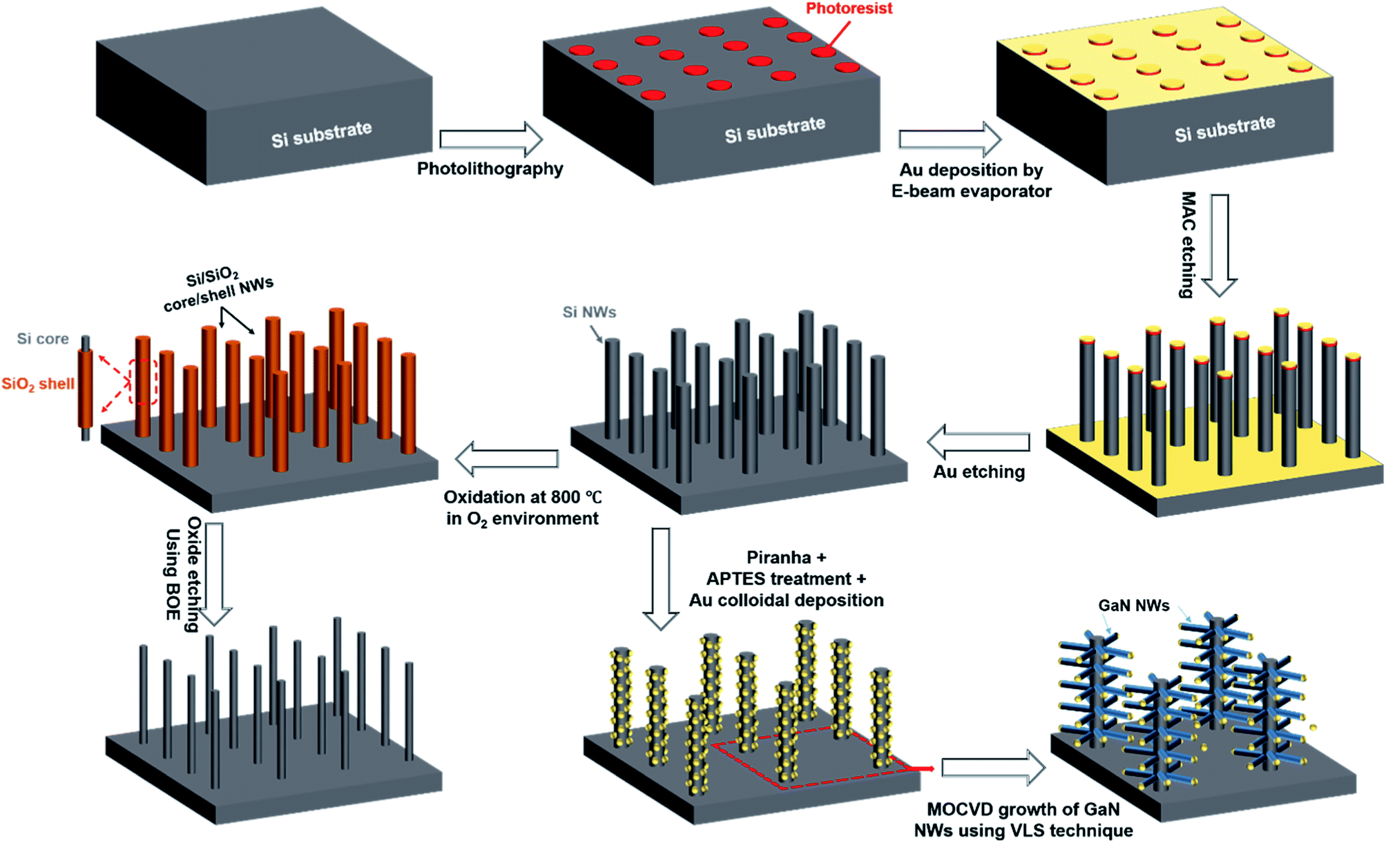 | ||
| Fig. 1 Schematic illustration of the process flow for the fabrication of the GaN/InGaN/Si hierarchical NWs and the diameter control of the Si NWs. | ||
2.2. Agglomeration of Au NPs on the Si NW-template
To grow GaN-based hierarchical NWs on the Si NW-template, the vapor–liquid–solid (VLS) growth technique was adopted using MOCVD. The metal catalyst required for the VLS growth is an important parameter that can control the density and dimensions of GaN NWs. Since vertically aligned Si NWs were used as the substrate, it was difficult to conformally deposit the metal shell on the sidewalls of the Si NWs with e-beam. Therefore, gold nanoparticles (NPs) were directly coated on the sidewalls of the Si NWs using a Au colloid solution (diameter = 14 nm). As the Au colloid NPs have negatively charged surfaces in order to prevent their aggregation, the Si NW substrate must undergo silanization treatment to create a positive charge prior to the coating. The samples underwent piranha treatment (H2SO4:H2O2 = 3:1) for 10 minutes which converted the surface of the Si NWs to a hydrophilic state and removed the remaining PR mask at the top of the NWs. Subsequently, the substrate was dipped in a (3-aminopropyl) triethoxysilane solution (APTES:methanol = 1:20) for 2 hours, rinsed with methanol, and heated at 120 °C for 15 minutes. Subsequently, the substrate was dipped in the Au colloid to coat Au NPs around the Si NWs due to the Coulomb attraction. The density of the coated Au NPs was controlled by adjusting the mixing ratio of the Au colloid and methanol, obtaining the controlled density of GaN NWs.35
2.3. Growth of GaN NWs and GaN/InGaN MQW NWs
Trimethylindium (TMIn) and trimethylgallium (TMGa) were introduced into a reactor at 550 °C and 650 °C, respectively, followed by their annealing at 850 °C for 1500 s to form a well-agglomerated Au/In/Ga metal alloy catalyst as reported in our previous study.7 The diameter of the Au NPs increased from 14 nm to ∼50 nm, and hence, the diameter of the GaN core NWs is controlled. Then, the precursors for gallium and nitrogen were introduced into the reactor, and the flow rates of TMGa and NH3 were 26.4 μmol min−1 and 3.125 mmol min−1, respectively, with a V/III ratio of 118. The carrier gas was H2 with a flow rate of 10.4 slm. After the VLS growth of the core GaN NWs, the lateral growth of the GaN shell was initiated by increasing the V/III ratio to 20000 using the vapor–solid (VS) growth mode. Then, the GaN barriers were grown laterally around the GaN shell with the TMGa and NH3 flow rates of 21.1 μmol min−1 and 402 mmol min−1, respectively. To grow InGaN QWs, the temperature was ramped down to 820 °C while the precursor for indium (TMIn = 51.75 μmol min−1) was also introduced. The growth time for the InGaN QWs was increased to 55 s, 110 s, and 165 s for samples (A), (B), and (C), respectively, while the total number of InGaN/GaN pairs was also optimized.
2.4. Structural and optical characterization
The patterning for the fabrication of Si NWs was conducted using a photolithography mask aligner (MDA 400 S UV). The dry etching was performed by inductively coupled plasma-reactive ion etching (VSICP 12 RC system). The Au film was deposited using an electron beam evaporator (World Vacuum, HVE-500A). The GaN/InGaN MQW NWs on the Si NWs were grown in a showerhead-based metal organic chemical vapor deposition system (CCS-FT 19 × 2 inch, Aixtron). The morphology of the Si NWs and GaN/InGaN MQW NWs was initially examined using a field emission scanning electron microscope (FE-SEM, JSM-6700F, Jeol). In-depth morphological analysis was conducted and the growth direction of GaN NWs was determined using a transmission electron microscope (JEM-2100F, Jeol). The reflectance was measured using a UV-vis spectrophotometer (Lambda 950 spectrometer, PerkinElmer). The room temperature PL spectrum of the 3-D hierarchical GaN/InGaN MQW NWs grown on the Si NW-template was recorded using a spectrometer (f = 0.5 m, Acton Research Co. spectrograph 500i), and an intensified CCD camera (P1-Max3) (Princeton Instrument) with a diode-pumped solid-state laser (Ekspla) with an excitation wavelength of 266 nm and a power of 11 mW. To measure the lifetime of photogenerated electron–hole pairs, TRPL study was carried out at a low temperature. The TRPL study was conducted with a 375 nm continuous-wave laser diode on the macroscale to deduce the PL efficiency. The temperatures of the samples were controlled from 18 K to 300 K in a closed helium cycle cryostat system. The TRPL spectra were measured with the second harmonic generation of a mode-locked Ti:sapphire laser (Coherent, Cameleon Ultra II) and a streak camera (Hamamatsu, C7700-01) for the examination of the temperature-dependent carrier dynamics. The pulse width, wavelength, and repetition rate of the pulsed laser were 200 fs, 375 nm, and 2 MHz, respectively. The temporal resolution of the time-resolved PL system was approximately 6 ps.3. Results and discussion
3.1. Growth and morphology evolution
Fig. 1 shows the schematics of the fabrication flow of the 3-D GaN-based hierarchical NWs grown on a Si NW-template. The Si NWs were fabricated by photolithography and MACE (using Au as the metal).36 Following the top-down growth of the Si NWs, their diameter was reduced by oxidization at 1000 °C for a controlled time which gave rise to the core/shell structure of the Si/SiO2 NWs. The SiO2 shell was etched using a buffer oxide etching solution. To grow GaN NWs on the Si NW-template, piranha and APTES treatment of the NWs was conducted. The piranha removed the organic residue while the APTES treatment generated positive polarity on the surface of the Si NWs. Colloidal Au (with negative charge) was attached to the Si NWs due to the attractive Coulomb force. The colloidal Au acted as a catalyst to facilitate the vapor–liquid–solid (VLS) growth of the GaN NWs.The length of the Si NWs was optimized by controlling the MACE time as shown in Fig. 2. Fig. 2(a–d) show the increased length of the Si NWs for the MACE times of 180, 360, 540, and 1200 s, respectively. The length of the Si NWs increased from 1.8 to 22 μm. The effect of MACE on the NW length is illustrated in greater detail in Fig. 2(e). To reduce their diameter, the Si NWs were oxidized, resulting in an increased diameter of the NWs with the Si/SiO2 core/shell structure as shown in Fig. 2(b-i). The shell was etched using a buffer oxide etching solution, and finally, the Si NWs were fabricated with a reduced diameter of less than 200 nm. To reduce the diameter, the samples were oxidized for 600 s and 1200 s as shown in Fig. 2(b-ii and b-iii), respectively. The minimum possible diameter is determined by the mechanical stability of the NWs, i.e. the NWs are broken or damaged when the diameter is very small. The criterion depends not only on diameter but height also plays a key role. Therefore, we can achieve a diameter thinner than 200 nm if we use shorter NWs as shown in Fig. 2(b-ii). As the oxidation time increases from a particular limit, all of the NWs transform to SiO2, and hence the top side is fully etched and the NWs evolve into a tapered shape as shown in Fig. 2(b-iii and b-iv). Therefore, this technique provides an approach for the fabrication of a patterned structure with precision which surpasses the limitations of the conventional photolithography used for the fabrication of Si-based structures.
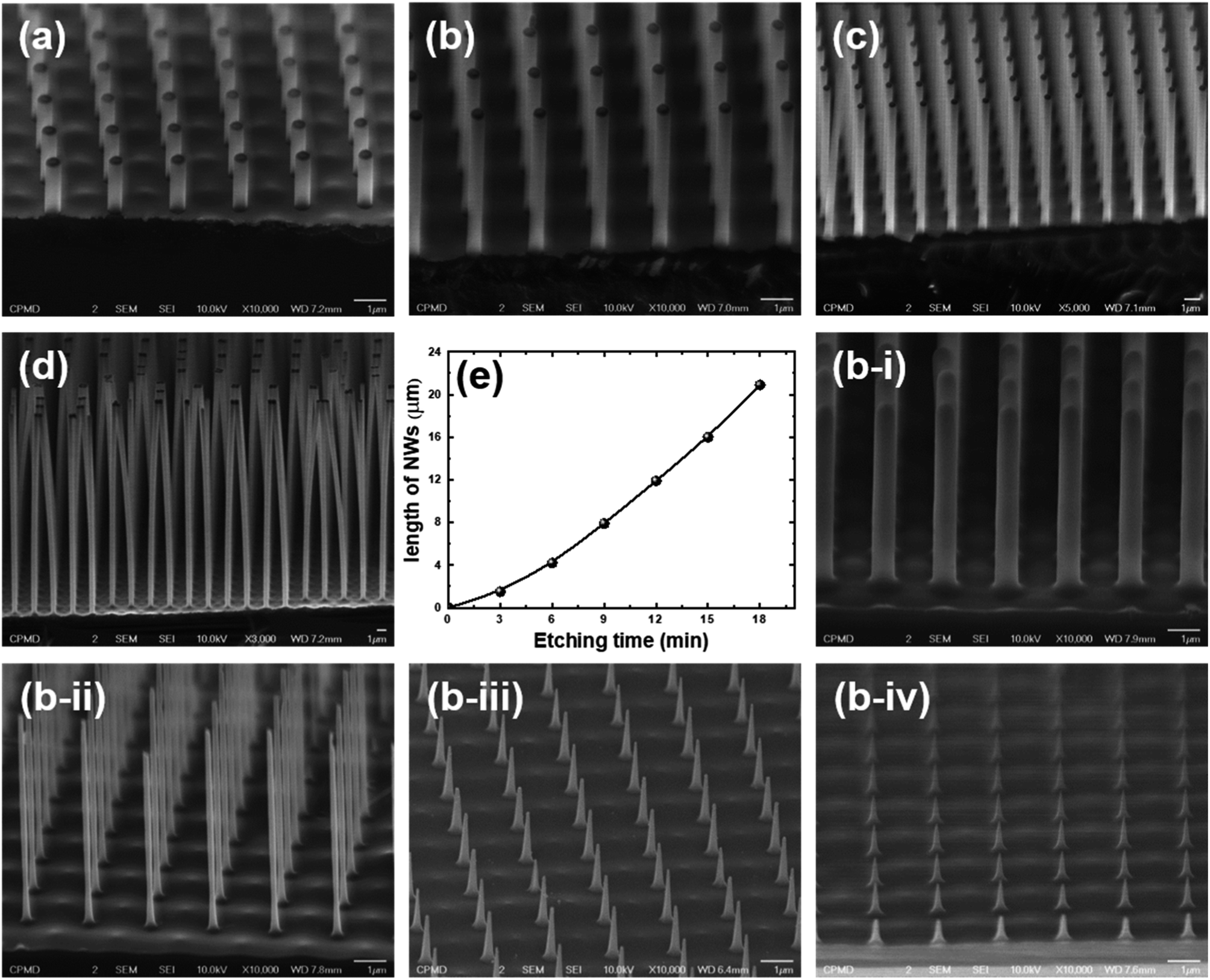 | ||
| Fig. 2 Scanning electron micrographs of the Si NWs with an etching time of (a) 3 min, (b) 6 min, (c) 9 min, and (d) 18 min. (e) The effect of the etching time on the Si NW length. (b-i) Wet thermal oxidation at 1000 °C, the images shown were captured after etching the oxide shell from the Si core; (b-ii) oxidation time of 10 min; (b-iii and b-iv) oxidation time of 20 min. | ||
Following the patterned growth of the Si NWs, the surface treatment of the Si NWs was carried out in order to deposit Au NPs. To elucidate the role of the surface treatment, the GaN NWs were grown with and without the APTES treatment. Fig. 3(a) shows the scanning electron micrograph of bare Si NWs after the piranha treatment which converted the surface to a hydrophilic state. The next step in the processing was to make the surface positively charged to enable the attachment of Au NPs to the Si NWs due to Coulomb interaction. Then, the GaN NWs were grown, and Fig. 3(b and c) show the SEM images of the samples fabricated without and with APTES treatment, respectively. Regarding the attachment of Au NPs on the Si NWs, a very clear difference is observed between the insets of Fig. 3(b and c). Hence, it is demonstrated that the APTES treatment enabled the surface to be more active for the attachment of Au NPs. The density of the GaN NWs can be controlled by optimizing the ratio of the Au colloid to the methanol solution.35 By reducing the melting temperature of the catalyst, the coverage of the Si NWs with GaN/InGaN MQWs can be increased. Additionally, indium incorporation into the NWs is enhanced at lower growth temperatures. Therefore, to reduce the melting temperature of the Au NPs, in situ deposition of very thin films of indium and gallium was carried out. Subsequent annealing resulted in the agglomeration of the Au/In/Ga metal-alloy catalyst with a low melting temperature, and high-density growth of the GaN NWs was achieved. After the axial growth of the GaN core NWs, the growth mode was switched to lateral growth by increasing the V/III ratio. The lateral growth of the GaN changed the geometry of the GaN NWs’ cross-section from circular to triangular. The smooth surface of the triangular-shaped GaN provided a high crystal quality platform for the growth of the active region of the InGaN/GaN MQW shells. A schematic diagram of the growth of the triangular-shaped MQW shells around the GaN core NWs on the Si NW-template is shown in Fig. 3(d), and the inset illustrates the growth of a single NW in more detail. The SEM photograph presented in Fig. 3(e) shows the 3-D hierarchical conformal growth of the GaN NWs on the Si NW-template using the Au/In/Ga metal-alloy spheres as a catalyst. It is observed from the inset that the growth of the GaN NWs started from all around the Si NW-template. Then, the InGaN/GaN MQW shells were grown and their SEM micrograph is shown in Fig. 3(f).
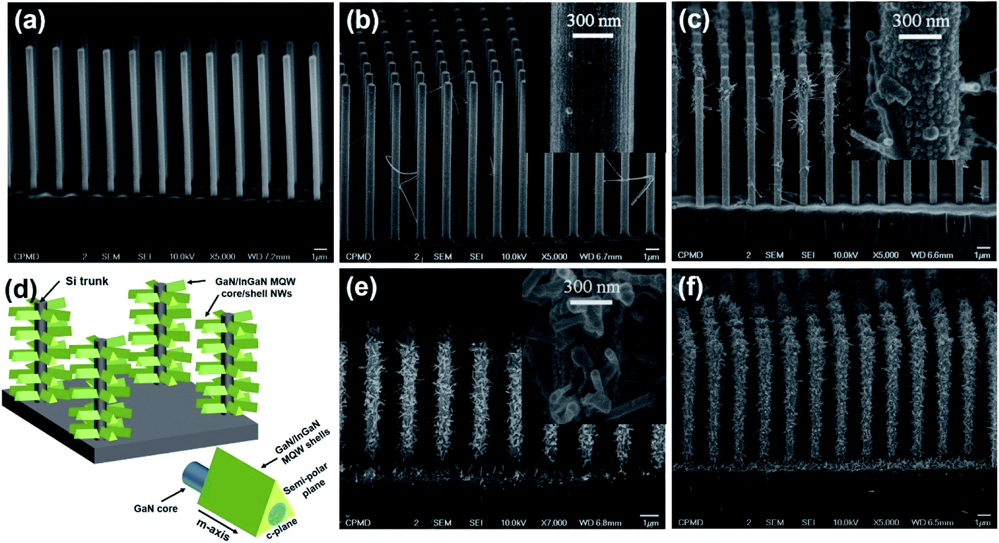 | ||
| Fig. 3 Optimization process for the Au colloid deposition and GaN-based NW-growth. (a) Scanning electron micrograph of the bare Si NWs and growth of the GaN NWs on the Si NW-template using Au NPs; the NPs were deposited (b) without the APTES treatment (the inset shows agglomerated NPs) and (c) with the APTES treatment but without indium and gallium deposition while the inset shows the agglomeration of the NPs and NW-growth. (d) Schematic illustration of the InGaN/GaN MQW NW shells around the GaN core NWs and the inset shows the cross-sectional view of the GaN core (circular) and the GaN/InGaN MQW shells (triangular shaped), (e) both APTES and In/Ga are used and the inset shows the NWs grown from the agglomerated NPs, and (f) growth of the GaN/InGaN/Si 3-D hierarchical NWs over a large area. | ||
To evaluate the growth direction and the crystal quality of the GaN NWs, transmission electron microscopy was conducted. The 3-D hierarchical NW-structure was cut using a doctor's blade and sonicated in ethanol, and then a drop of this solution was poured onto a TEM grid. A low-resolution TEM micrograph of the 3-D hierarchical structure over a single Si NW is shown in Fig. 4(a). Several GaN NWs were separated from the Si trunk during the sonication, and therefore, high-density branches are not observed unlike in the images observed by SEM. A single GaN-based NW is presented in Fig. 4(b) in order to examine the overall surface smoothness. A high-resolution image of the same NW is presented in Fig. 4(c), showing an interplanar spacing of 0.28 nm which is ascribed to the m-axial growth direction of the GaN core NWs. To verify that the growth direction is along the m-axis, selected area electron diffraction (SAED) patterns were also measured. The SAED patterns confirm the same growth direction as shown in Fig. 4(d). The zone axis of the electron beam was the  plane and the growth direction was toward the [1
![[1 with combining macron]](https://www.rsc.org/images/entities/char_0031_0304.gif) 00] plane. Here, it is very important to mention about the controlled growth direction of GaN core NWs on all host facets of the Si trunk. It was verified by conducting TEM for several samples, and all the time, the growth direction was m-axial. It is possible to optimize the growth direction of GaN NWs during VLS growth mode by controlling the catalyst composition even on a polycrystalline substrate.37 A triangular cross-section of the GaN/InGaN MQW NWs is observed which is attributed to the (112) semi-polar growth direction of the GaN/InGaN MQW shells, with the schematics shown in Fig. 4(e and f), as it was observed in our previous publications.26,37 The optical properties of the active region grown on the semi-polar plane are enhanced when the inclination angle of the polar-plane to the semi-polar growth plane ranges from 45° to 60°. For the incorporation of indium into the InGaN QWs, over a wide range of growth temperatures, the most favorable planes are (112) and (101). Among these, the surface of the (112) semi-polar plane exhibits the highest indium incorporation rates.38 The triangular-shape evolution of the GaN/InGaN MQW coaxial NWs can be understood with the help of kinetic Wulff plots known as ν-plots. After the growth of the GaN core NWs, the lateral growth starts together with the competition between all of the planes perpendicular to the m-axis with the fast-growing planes growing to extinction while the slower-growing planes define the final shape.39,40 In this case, the growth rate of the (000) plane is the slowest while the (112) is the second-slowest-growing plane, with the convex geometry of NWs making the slowest growing planes appear on the sidewalls of the GaN core NWs. Therefore, this is an appropriate approach for understanding the sidewall evolution of the shell growth mechanism around the GaN core NWs.
00] plane. Here, it is very important to mention about the controlled growth direction of GaN core NWs on all host facets of the Si trunk. It was verified by conducting TEM for several samples, and all the time, the growth direction was m-axial. It is possible to optimize the growth direction of GaN NWs during VLS growth mode by controlling the catalyst composition even on a polycrystalline substrate.37 A triangular cross-section of the GaN/InGaN MQW NWs is observed which is attributed to the (112) semi-polar growth direction of the GaN/InGaN MQW shells, with the schematics shown in Fig. 4(e and f), as it was observed in our previous publications.26,37 The optical properties of the active region grown on the semi-polar plane are enhanced when the inclination angle of the polar-plane to the semi-polar growth plane ranges from 45° to 60°. For the incorporation of indium into the InGaN QWs, over a wide range of growth temperatures, the most favorable planes are (112) and (101). Among these, the surface of the (112) semi-polar plane exhibits the highest indium incorporation rates.38 The triangular-shape evolution of the GaN/InGaN MQW coaxial NWs can be understood with the help of kinetic Wulff plots known as ν-plots. After the growth of the GaN core NWs, the lateral growth starts together with the competition between all of the planes perpendicular to the m-axis with the fast-growing planes growing to extinction while the slower-growing planes define the final shape.39,40 In this case, the growth rate of the (000) plane is the slowest while the (112) is the second-slowest-growing plane, with the convex geometry of NWs making the slowest growing planes appear on the sidewalls of the GaN core NWs. Therefore, this is an appropriate approach for understanding the sidewall evolution of the shell growth mechanism around the GaN core NWs.
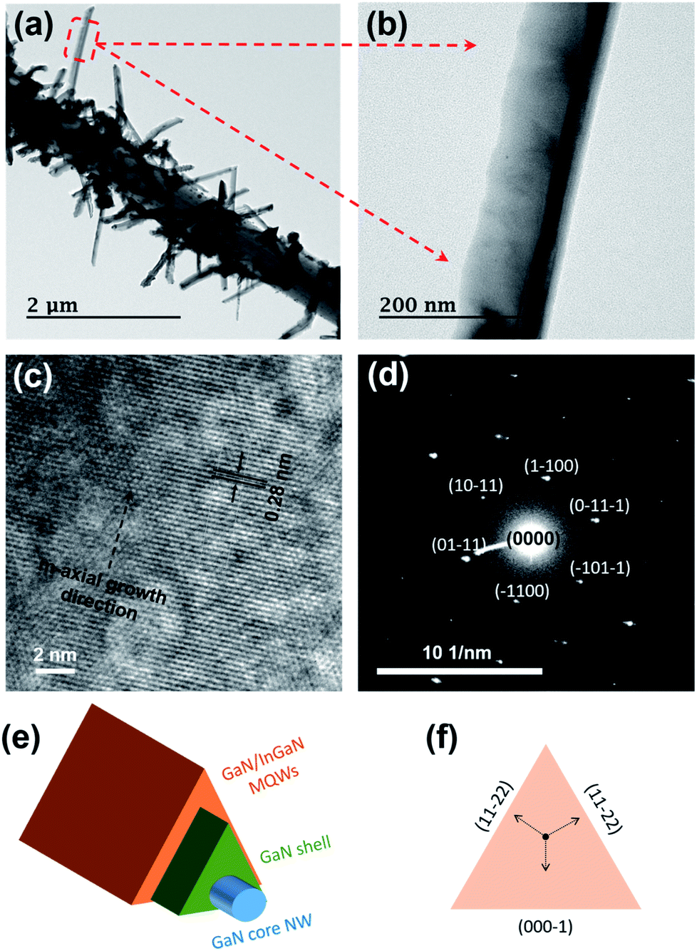 | ||
| Fig. 4 Transmission electron microscopy image of the GaN/InGaN MQW NWs on the Si trunk. (a) Low-magnification TEM image, (b) high-magnification image of a single GaN/InGaN MQW NW, (c) high-resolution image of the respective NWs, depicting the interplanar spacing of the planes along the growth direction of the GaN core NWs, and (d) SAED patterns showing the growth direction of the core NWs along the m-axis. (e) Schematic illustration of the geometry of GaN core NWs and the triangular shells around the core and (f) the growth direction of evolved facets of triangular shells around GaN core NWs. | ||
3.2. Optical properties of 3-D hierarchical GaN/InGaN/Si MQW NWs
Efficient absorption of light is vital for enhanced device applications. The high measured reflectance is one of the many parameters that may reduce the device efficiency. In this regard, suppression of the reflectance is highly important for a variety of optical applications. Therefore, the reflectance of the 3-D hierarchical GaN/InGaN MQW NWs grown on the Si NWs was measured to demonstrate the potential of this unique morphology. The reflectance was measured at the wavelengths between 350 and 800 nm. Fig. 5(a) shows the results of the reflectance measurements of the bare Si substrate, Si NW-templates with different lengths and the samples obtained after the growth of the 3-D hierarchical GaN/InGaN MQW NWs on the Si NW-template. The difference between the reflectance values for the bare Si substrate and the 3-D hierarchical GaN/InGaN MQW NWs on the Si NW-template is as high as 35% for the entire visible region. Hence, the 3-D hierarchical GaN/InGaN MQW NWs grown on the Si NW-template provide a favorable medium for efficient light absorption. Initially, the optical emission from the 3-D hierarchical GaN/InGaN MQW NWs grown on the Si NW-template was evaluated using room temperature PL. The excitation wavelength and optical power of the laser were 266 nm and 11 mW, respectively. To optimize the emission intensity from the active region of GaN/InGaN MQWs, the number of QW pairs was varied as 5, 7, and 9 (the obtained emission profile is described in the ESI†), and it was found that the integrated intensity increased with the number of QWs. Among these, the sample having 5 pairs of QWs was chosen for tuning the emission spectrum. To demonstrate the high crystal quality of the GaN/InGaN MQW NWs even at longer emission wavelengths, the number of pairs with low emission intensity was fixed (5 pairs). To tune the emission profile, the InGaN QW thickness was increased from sample (A) to sample (C) and the emission profile was measured at room temperature using PL as shown in Fig. 5(b). The central wavelength of the peaks was measured as 448 nm, 476 nm, and 503 nm for samples (A), (B), and (C), respectively. Due to quantum confinement, the emission peak shifted to longer wavelengths with increased QW thickness. Peak broadening and the characteristic yellow luminescence were not observed for all of the samples, indicating the high crystal quality of the GaN/InGaN MQW NWs grown on the Si NW-template. Furthermore, the band-to-band transition of GaN was not observed, providing proof of the full coverage of the GaN core NWs with the GaN/InGaN MQWs from top to bottom.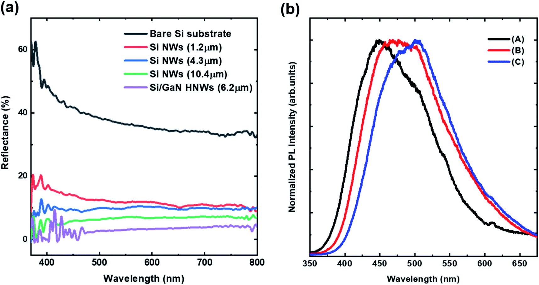 | ||
| Fig. 5 (a) The effect of NWs' morphology on reflectance and (b) room temperature PL measurements. | ||
3.3. Carrier dynamics of 3-D hierarchical NWs
The carrier lifetime of the photogenerated carriers of the 3-D hierarchical semi-polar GaN/InGaN MQW NWs grown on the Si NW-template was measured using temperature-dependent time-resolved PL (TRPL). The excitation source was a 375 nm continuous wave laser diode while the temperature was varied in the 18–300 K range using a closed helium cycle cryostat system. The TRPL spectra were measured with the second harmonic generation of a mode-locked Ti:sapphire laser (Coherent, Cameleon Ultra II) and a streak camera (Hamamatsu, C7700-01) for low-temperature carrier dynamics. The wavelength, pulse width, and repetition rate of the pulsed laser were 375 nm, 200 fs, and 2 MHz, respectively. The temporal resolution of the time-resolved PL system was approximately 6 ps. The temperature-dependent temporal decay curves measured using TRPL of samples (A), (B), and (C) are shown in Fig. 6(a–c), respectively. The stretched exponential model given in eqn (1) provides the best method for estimating the lifetime of the carriers of a system with a non-single decay.| I(t) = Ioexp[−(t/τ)β], | (1) |
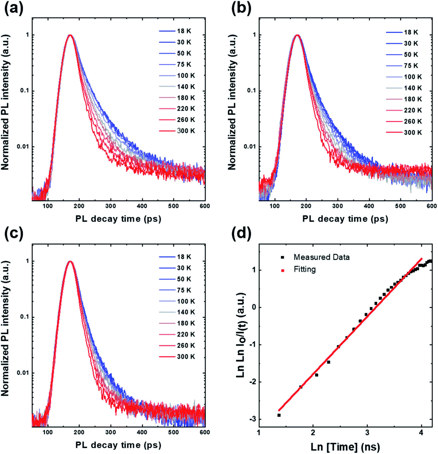 | ||
| Fig. 6 Temperature-dependent TRPL of (a) sample (A), (b) sample (B), and (c) sample (C). (d) Demonstration of the fitting using the stretched exponential model on sample (A) at 18 K. | ||
| Sample name | QW thickness, dQW (nm) | Time constant at 300 K, τ300 K (ps) | Radiative lifetime, τr (ps) | Nonradiative lifetime, τnr (ps) | IQE, (%) | Stretching constant, β |
|---|---|---|---|---|---|---|
| (A) | 0.6 | 19.4 | 34.8 | 43.8 | 55.8 | 0.77 |
| (B) | 1.2 | 17.2 | 31.4 | 37.9 | 54.6 | 0.75 |
| (C) | 1.8 | 14.5 | 30.7 | 27.5 | 47.2 | 0.72 |
To understand the overall carrier dynamics of the hybrid structure of the 3-D hierarchical GaN/InGaN MQW NWs grown on the Si NW-template, temporal decay maps (TDMs) were recorded as a function of the emission wavelength over time. The TDMs of all of the samples were recorded at 18, 30, 50, 75, 100, 140, 180, 220, 260, and 300 K. The TDMs measured at all of these temperatures are shown in Fig. 7 while the TDMs of samples (B) and (C) are described in the ESI.† A redshift in the tails of TDMs is observed with increased QW thickness while the tail shows the carriers with a long lifetime. The underlying phenomena for the redshift can be described using the model proposed by Minsky et al. and Chichibu et al.41,42 According to this model, the radiative recombination in InGaN QWs can occur either through free-exciton or bound-exciton transitions. For thin InGaN QWs, only the free-exciton recombination mechanism is possible while the localized states are formed due to the indium concentration fluctuations inside the thick QWs which lead to the radiative recombination through bound excitons. It is well-known that the lifetime of the radiative transitions through free excitons is longer than that through the bound- or localized-excitons. Therefore, the results of the TDMs recorded with increased QW thickness are in good agreement with the results of TDCs.
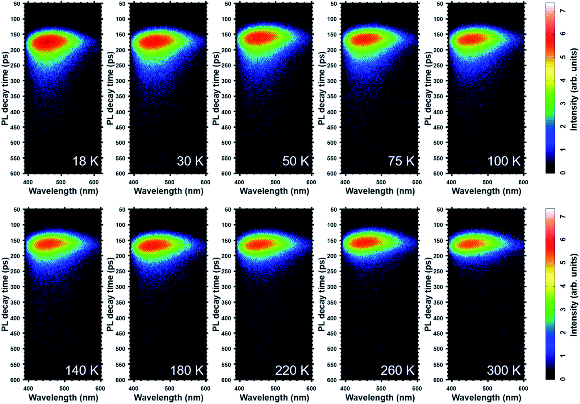 | ||
| Fig. 7 Temperature-dependent temporal decay maps of sample (A). | ||
The emission wavelength-dependent PL decay rates as a function of the measurement temperature are recorded in the TDMs and shown in Fig. 7 for sample (A). The tail of the TDMs at low temperatures is more prominent than that for the room temperature measurements. The underlying reason for the shortened lifetime of the carriers at room temperature can be explained by the potential distribution of the carriers. Due to indium concentration fluctuations inside the InGaN QWs, weakly localized and strongly localized states are formed. The carrier escape and capture at low temperature are inefficient so that the carrier transport is inefficient. As the temperature increases, the carriers' escape from the weakly localized states becomes efficient and the carriers are relaxed by the strongly localized states via hopping. Then, as the temperature is increased further and reaches the value near room temperature, carrier thermalization occurs in strongly localized states and leads to carrier escape, so that the decay tail decreases over time as shown in the TDM measured at 300 K in Fig. 7. Hence, the results of the TDM analysis are in good agreement with our previous discussion based on the results of TDCs.
To demonstrate the broader aspect of the influence of QW thickness on carrier dynamics as a function of the measurement temperature, the TDCs measured at 18 K and 300 K are explicitly shown in Fig. 8(a and b), respectively. The decay constant was measured using a single exponential model and a stretched exponential model. The time constant obtained (18 to 300 K) using the single exponential model for samples (A), (B), and (C) varied from 28 to 19 ps, from 25 to 19 ps, and from 22 to 17 ps, respectively, as shown in Fig. 8(c). The time constant obtained (18 to 300 K) using the stretched exponential model for samples (A), (B), and (C) varied from 35 to 19 ps, from 31 to 17 ps, and from 28 to 15 ps, respectively, as shown in Fig. 8(d). The optical results of TDCs and TDMs are in good agreement with each other, indicating the high crystal quality of the 3-D hierarchical GaN/InGaN MQW NWs for a variety of optical and electronic applications.
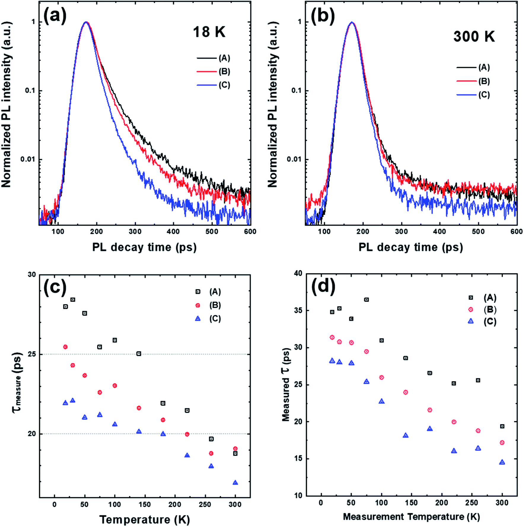 | ||
| Fig. 8 TRPL measurements of all of the samples at (a) 18 K and (b) 300 K. Calculations of the time constant with the measurement temperature and QW thickness using (c) the single exponential model and (d) the stretched exponential model. | ||
4. Conclusions
In summary, a facile and scalable route for the fabrication of next-generation 3-D hierarchical GaN/InGaN/Si NWs using a simple two-step growth mechanism by MOCVD on patterned Si NWs is reported. The Si NWs were fabricated by photolithography and the final diameter of the obtained Si NWs was as high as 200 nm. Then, the nonpolar [100] GaN NWs were grown around the Si NW-trunk, and the growth axis of GaN core NWs was optimized using a controlled catalyst composition. The lateral growth of the GaN/InGaN MQW shells around the GaN core NWs was conducted by increasing the V/III ratio and their growth was carried out on the semi-polar growth facet which leads to the suppressed QCSE. The optical emission was tuned from 440 to 505 nm by increasing the InGaN QW thickness. The carrier dynamics were evaluated by conducting low-temperature TRPL measurement. An ultrashort carrier lifetime in the 28–35 ps range was measured together with an IQE of 56%. Such a high IQE is achieved due to the reduced reflectance and the semi-polar growth facet of the GaN/InGaN MQW structure. The comprehensive analysis of TDCs and TDMs confirmed the high crystal quality of the 3-D hierarchical GaN/InGaN/Si MQW NWs which enables their use in a wide range of next-generation optical and electronic applications.
Conflicts of interest
The authors declare no competing financial interest.Acknowledgements
This work was supported by the National Research Foundation of Korea (NRF) funded by the Ministry of Education, Science, and Technology (2018R1A6A1A03024334, NRF-2019R1A2C1006360). The samples were grown by using MOCVD (Aixtron-CS15276) at the Energy Convergence Core Facility in Chonnam National University, Gwangju, South Korea.References
- J. Claudon, J. Bleuse, N. S. Malik, M. Bazin, P. Jaffrennou, N. Gregersen, C. Sauvan, P. Lalanne and J.-M. Gérard, A highly efficient single-photon source based on a quantum dot in a photonic nanowire, Nat. Photonics, 2010, 4, 174–177, DOI:10.1038/nphoton.2009.287x.
- X. Miao, Promising single-photon emitters with reconfined InGaN/GaN nanowire quantum dots, Quantum Engineering, 2019, 1(3), e21, DOI:10.1002/que2.21.
- Y. Xiao, C. Meng, P. Wang, Y. Ye, H. Yu, S. Wang, F. Gu, L. Dai and L. Tong, Single-Nanowire Single-Mode Laser, Nano Lett., 2011, 11, 1122–1126, DOI:10.1021/nl1040308.
- S. M. Sadaf, Y. H. Ra, T. Szkopek and Z. Mi, Monolithically Integrated Metal/Semiconductor Tunnel Junction Nanowire Light-Emitting Diodes, Nano Lett., 2016, 16, 1076–1080, DOI:10.1021/acs.nanolett.5b04215.
- R. Yan, J.-H. Park, Y. Choi, C.-J. Heo, S.-M. Yang, L. P. Lee and P. Yang, Nanowire-based single-cell endoscopy, Nat. Nanotechnol., 2012, 7, 191–196, DOI:10.1038/nnano.2011.226.
- M.-A. Doucey and S. Carrara, Nanowire Sensors in Cancer, Trends Biotechnol., 2019, 37, 86–99, DOI:10.1016/j.tibtech.2018.07.014.
- M. A. Johar, A. Waseem, M. A. Hassan, J.-H. Kang, J.-S. Ha, J. K. Lee and S.-W. Ryu, Facile growth of high aspect ratio c-axis GaN nanowires and their application as flexible p–n NiO/GaN piezoelectric nanogenerators, Acta Mater., 2018, 161, 237–245, DOI:10.1016/j.actamat.2018.09.030.
- M. Johar, M. Hassan, A. Waseem, J.-S. Ha, J. Lee and S.-W. Ryu, Stable and High Piezoelectric Output of GaN Nanowire-Based Lead-Free Piezoelectric Nanogenerator by Suppression of Internal Screening, Nanomaterials, 2018, 8, 437, DOI:10.3390/nano8060437.
- A. Waseem, M. A. Johar, M. A. Hassan, I. V. Bagal, J.-S. Ha, J. K. Lee and S.-W. Ryu, Effect of crystal orientation of GaN/V2O5 core-shell nanowires on piezoelectric nanogenerators, Nano Energy, 2019, 60, 413–423, DOI:10.1016/j.nanoen.2019.03.075.
- L. Zhang, T. Wang, L. Sun, Y. Sun, T. Hu, K. Xu and F. Ma, Hydrothermal synthesis of 3D hierarchical MoSe2/NiSe2 composite nanowires on carbon fiber paper and their enhanced electrocatalytic activity for the hydrogen evolution reaction, J. Mater. Chem. A, 2017, 5, 19752–19759, 10.1039/C7TA05352E.
- Y. K. A. Lau, D. J. Chernak, M. J. Bierman and S. Jin, Epitaxial growth of hierarchical PbS nanowires, J. Mater. Chem., 2009, 19, 934–940, 10.1039/B818187J.
- J. Moon, U. Sim, D. J. Kim, H.-Y. Ahn, J. An, H. Ha, K. S. Choi, C. Jeon, J. Lee, K. T. Nam and B. H. Hong, Hierarchical carbon–silicon nanowire heterostructures for the hydrogen evolution reaction, Nanoscale, 2018, 10, 13936–13941, 10.1039/C8NR02262C.
- Y. J. Hwang, C. H. Wu, C. Hahn, H. E. Jeong and P. Yang, Si/InGaN Core/Shell Hierarchical Nanowire Arrays and their Photoelectrochemical Properties, Nano Lett., 2012, 12, 1678–1682, DOI:10.1021/nl3001138.
- S. Huang, B. He, X. Yan, I. Khan, J. Wang, M. Gao, J. Lan, S. Li and J. Kang, Hierarchical ZnO/Si nanowire arrays as an effective substrate for surface-enhanced Raman scattering application, Sens. Actuators, B, 2018, 273, 48–55, DOI:10.1016/j.snb.2018.06.003.
- J. Shi and X. Wang, Hierarchical TiO2–Si nanowire architecture with photoelectrochemical activity under visible light illumination, Energy Environ. Sci., 2012, 5, 7918–7922, 10.1039/C2EE22113F.
- A. K. Singh and D. Sarkar, A facile approach for preparing densely-packed individual p-NiO/n-Fe2O3 heterojunction nanowires for photoelectrochemical water splitting, Nanoscale, 2018, 10, 13130–13139, 10.1039/C8NR02508H.
- M. A. Hassan, M. A. Johar, S. Y. Yu and S.-W. Ryu, Facile Synthesis of Well-Aligned ZnO Nanowires on Various Substrates by MOCVD for Enhanced Photoelectrochemical Water-Splitting Performance, ACS Sustainable Chem. Eng., 2018, 6, 16047–16054, DOI:10.1021/acssuschemeng.8b02392.
- S. Gopalakrishnan and K. Jeganathan, Facile fabrication of silicon nanowires as photocathode for visible-light induced photoelectrochemical water splitting, Int. J. Hydrogen Energy, 2017, 42, 22671–22676, DOI:10.1016/j.ijhydene.2017.07.148.
- S. M. Thalluri, J. Borme, D. Xiong, J. Xu, W. Li, I. Amorim, P. Alpuim, J. Gaspar, H. Fonseca, L. Qiao and L. Liu, Highly-ordered silicon nanowire arrays for photoelectrochemical hydrogen evolution: an investigation on the effect of wire diameter, length and inter-wire spacing, Sustainable Energy Fuels, 2018, 2, 978–982, 10.1039/C7SE00591A.
- S. M. Sadaf, S. Zhao, Y. Wu, Y.-H. Ra, X. Liu, S. Vanka and Z. Mi, An AlGaN Core–Shell Tunnel Junction Nanowire Light-Emitting Diode Operating in the Ultraviolet-C Band, Nano Lett., 2017, 17, 1212–1218, DOI:10.1021/acs.nanolett.6b05002.
- S.-W. Ryu, J. Park, J.-K. Oh, D. H. Long, K.-W. Kwon, Y.-H. Kim, J. K. Lee and J. H. Kim, Analysis of Improved Efficiency of InGaN Light-Emitting Diode With Bottom Photonic Crystal Fabricated by Anodized Aluminum Oxide, Adv. Funct. Mater., 2009, 19, 1650–1655, DOI:10.1002/adfm.200801125.
- A. S. A. Fletcher and D. Nirmal, A survey of Gallium Nitride HEMT for RF and high power applications, Superlattices Microstruct., 2017, 109, 519–537, DOI:10.1016/j.spmi.2017.05.042.
- M. A. Johar, J.-H. Kang, M. A. Hassan and S.-W. Ryu, A scalable, flexible and transparent GaN based heterojunction piezoelectric nanogenerator for bending, air-flow and vibration energy harvesting, Appl. Energy, 2018, 222, 781–789, DOI:10.1016/j.apenergy.2018.04.038.
- C. Zhao, T. K. Ng, R. T. ElAfandy, A. Prabaswara, G. B. Consiglio, I. A. Ajia, I. S. Roqan, B. Janjua, C. Shen, J. Eid, A. Y. Alyamani, M. M. El-Desouki and B. S. Ooi, Droop-Free, Reliable, and High-Power InGaN/GaN Nanowire Light-Emitting Diodes for Monolithic Metal-Optoelectronics, Nano Lett., 2016, 16, 4616–4623, DOI:10.1021/acs.nanolett.6b01945.
- M. Tchernycheva, P. Lavenus, H. Zhang, A. V. Babichev, G. Jacopin, M. Shahmohammadi, F. H. Julien, R. Ciechonski, G. Vescovi and O. Kryliouk, InGaN/GaN Core–Shell Single Nanowire Light Emitting Diodes with Graphene-Based P-Contact, Nano Lett., 2014, 14, 2456–2465, DOI:10.1021/nl5001295.
- M. A. Johar, H.-G. Song, A. Waseem, J.-H. Kang, J.-S. Ha, Y.-H. Cho and S.-W. Ryu, Ultrafast carrier dynamics of conformally grown semi-polar (112) GaN/InGaN multiple quantum well co-axial nanowires on m-axial GaN core nanowires, Nanoscale, 2019, 11, 10932–10943, 10.1039/C9NR02823D.
- H. Li, M. Khoury, B. Bonef, A. I. Alhassan, A. J. Mughal, E. Azimah, M. E. A. Samsudin, P. De Mierry, S. Nakamura, J. S. Speck and S. P. DenBaars, Efficient Semipolar (11–22) 550 nm Yellow/Green InGaN Light-Emitting Diodes on Low Defect Density (11–22) GaN/Sapphire Templates, ACS Appl. Mater. Interfaces, 2017, 9, 36417–36422, DOI:10.1021/acsami.7b11718.
- S. Yamamoto, Y. Zhao, C.-C. Pan, R. B. Chung, K. Fujito, J. Sonoda, S. P. DenBaars and S. Nakamura, High-Efficiency Single-Quantum-Well Green and Yellow-Green Light-Emitting Diodes on Semipolar (2021) GaN Substrates, Appl. Phys. Express, 2010, 3, 122102, DOI:10.1143/APEX.3.122102.
- N. Poyiatzis, M. Athanasiou, J. Bai, Y. Gong and T. Wang, Monolithically integrated white light LEDs on (11–22) semi-polar GaN templates, Sci. Rep., 2019, 9, 1383, DOI:10.1038/s41598-018-37008-5.
- Y. Zhang, R. M. Smith, Y. Hou, B. Xu, Y. Gong, J. Bai and T. Wang, Stokes shift in semi-polar ( 112) InGaN/GaN multiple quantum wells, Appl. Phys. Lett., 2016, 108, 031108, DOI:10.1063/1.4940396.
- T. Wang, Topical Review: Development of overgrown semi-polar GaN for high efficiency green/yellow emission, Semicond. Sci. Technol., 2016, 31, 093003, DOI:10.1088/0268-1242/31/9/093003.
- C. Li, J. B. Wright, S. Liu, P. Lu, J. J. Figiel, B. Leung, W. W. Chow, I. Brener, D. D. Koleske, T.-S. Luk, D. F. Feezell, S. R. J. Brueck and G. T. Wang, Nonpolar InGaN/GaN Core–Shell Single Nanowire Lasers, Nano Lett., 2017, 17, 1049–1055, DOI:10.1021/acs.nanolett.6b04483.
- W. Song, R. Wang, X. Wang, D. Guo, H. Chen, Y. Zhu, L. Liu, Y. Zhou, Q. Sun, L. Wang and S. Li, a-Axis GaN/AlN/AlGaN Core–Shell Heterojunction Microwires as Normally Off High Electron Mobility Transistors, ACS Appl. Mater. Interfaces, 2017, 9, 41435–41442, DOI:10.1021/acsami.7b12986.
- J. Lähnemann, A. Ajay, M. I. Den Hertog and E. Monroy, Near-Infrared Intersubband Photodetection in GaN/AlN Nanowires, Nano Lett., 2017, 17, 6954–6960, DOI:10.1021/acs.nanolett.7b03414.
- J.-H. Kang, M. Ali Johar, B. Alshehri, E. Dogheche and S.-W. Ryu, Facile growth of density- and diameter-controlled GaN nanobridges and their photodetector application, J. Mater. Chem. C, 2017, 5, 11879–11884, 10.1039/C7TC02619F.
- I. V. Bagal, M. A. Johar, M. A. Hassan, A. Waseem and S.-W. Ryu, Facile morphology control of high aspect ratio patterned Si nanowires by metal-assisted chemical etching, J. Mater. Sci.: Mater. Electron., 2018, 29, 18167–18177, DOI:10.1007/s10854-018-9929-8.
- M. A. Johar, H.-G. Song, A. Waseem, M. A. Hassan, I. V. Bagal, Y.-H. Cho and S.-W. Ryu, Universal and scalable route to fabricate GaN nanowire-based LED on amorphous substrate by MOCVD, Appl. Mater. Today, 2020, 19, 100541, DOI:10.1016/j.apmt.2019.100541.
- Y. Zhao, Q. Yan, C.-Y. Huang, S.-C. Huang, P. Shan Hsu, S. Tanaka, C.-C. Pan, Y. Kawaguchi, K. Fujito, C. G. Van de Walle, J. S. Speck, S. P. DenBaars, S. Nakamura and D. Feezell, Indium incorporation and emission properties of nonpolar and semipolar InGaN quantum wells, Appl. Phys. Lett., 2012, 100, 201108, DOI:10.1063/1.4719100.
- B. Leung, Q. Sun, C. D. Yerino, J. Han and M. E. Coltrin, Using the kinetic Wulff plot to design and control nonpolar and semipolar GaN heteroepitaxy, Semicond. Sci. Technol., 2012, 27, 024005, DOI:10.1088/0268-1242/27/2/024005.
- J. Song, J. Choi, C. Zhang, Z. Deng and Y. Xie, J. Han, Elimination of Stacking Faults in Semipolar GaN and Light-Emitting Diodes Grown on Sapphire, ACS Appl. Mater. Interfaces, 2019, 11, 33140–33146, DOI:10.1021/acsami.9b11316.
- M. S. Minsky, S. Watanabe and N. Yamada, Radiative and nonradiative lifetimes in GaInN/GaN multiquantum wells, J. Appl. Phys., 2002, 91, 5176–5181, DOI:10.1063/1.1459106.
- Sf. Chichibu, T. Onuma, T. Sota, S. P. DenBaars, S. Nakamura, T. Kitamura, Y. Ishida and H. Okumura, Influence of InN mole fraction on the recombination processes of localized excitons in strained cubic InxGa1–xN/GaN multiple quantum wells, J. Appl. Phys., 2003, 93, 2051–2054, DOI:10.1063/1.1535746.
Footnotes |
| † Electronic supplementary information (ESI) available. See DOI: 10.1039/d0na00115e |
| ‡ M. A. Johar and T. Kim contributed equally. |
| This journal is © The Royal Society of Chemistry 2020 |