
 Open Access Article
 This Open Access Article is licensed under a Creative Commons Attribution-Non Commercial 3.0 Unported Licence
Research progress on solutions to the sneak path issue in memristor crossbar arrays
Lingyun
Shi
a,
Guohao
Zheng
a,
Bobo
Tian
 *ab,
Brahim
Dkhil
b and
Chungang
Duan
ac
*ab,
Brahim
Dkhil
b and
Chungang
Duan
ac
aDepartment of Electronics, Key Laboratory of Polar Materials and Devices (MOE), East China Normal University, Shanghai 200241, China. E-mail: bbtian@ee.ecnu.edu.cn
bLaboratoire Structures, Propriétés et Modélisation des Solides, CentraleSupélec, CNRS-UMR8580, Université Paris-Saclay, 91190 Gif-sur-Yvette, France
cCollaborative Innovation Center of Extreme Optics, Shanxi University, Shanxi 030006, China
First published on 11th March 2020
Abstract
Since the emergence of memristors (or memristive devices), how to integrate them into arrays has been widely investigated. After years of research, memristor crossbar arrays have been proposed and realized with potential applications in nonvolatile memory, logic and neuromorphic computing systems. Despite the promising prospects of memristor crossbar arrays, one of the main obstacles for their development is the so-called sneak-path current causing cross-talk interference between adjacent memory cells and thus may result in misinterpretation which greatly influences the operation of memristor crossbar arrays. Solving the sneak-path current issue, the power consumption of the array will immensely decrease, and the reliability and stability will simultaneously increase. In order to suppress the sneak-path current, various solutions have been provided. So far, some reviews have considered some of these solutions and established a sophisticated classification, including 1D1M, 1T1M, 1S1M (D: diode, M: memristor, T: transistor, S: selector), self-selective and self-rectifying memristors. Recently, a mass of studies have been additionally reported. This review thus attempts to provide a survey on these new findings, by highlighting the latest research progress realized for relieving the sneak-path issue. Here, we first present the concept of the sneak-path current issue and solutions proposed to solve it. Consequently, we select some typical and promising devices, and present their structures and properties in detail. Then, the latest research activities focusing on single-device structures are introduced taking into account the mechanisms underlying these devices. Finally, we summarize the properties and perspectives of these solutions.
 Lingyun Shi | Lingyun Shi is an undergraduate student of East China Normal University, and Key Laboratory of Polar Materials and Devices, Ministry of Education, majoring in Microelectronics Science and Engineering. His research interests include the design and analysis of nanostructures of memristor crossbar arrays, optical devices and radio frequency integrated circuits. Relevant studies have been published in Opt. Commun. |
 Bobo Tian | Bobo Tian earned his Ph.D. in Microelectronics and Solid-State Electronics from the University of Chinese Academy of Sciences, Beijing, China and CentraleSupélec, Université Paris-Saclay, Paris, France in 2016. Then he performed post-doctoral research at East China Normal University and CentraleSupélec, Université Paris-Saclay. He is now a young researcher at the Key Lab of Polar Materials and Devices (MOE), East China Normal University, China. His group is currently working on ferroelectrics, memristors, and neuromorphic computing. He has published over 50 papers in journals such as Nat. Electron., Nat. Commun., Adv. Electron. Mater., Appl. Phys. Lett., and Phys. Rev. B. |
 Brahim Dkhil | Brahim Dkhil earned his Ph.D. in Materials Science from the University of Orsay and Ecole Centrale Paris, France in 1999. Then he worked as a researcher at Ecole Centrale Paris. He also worked as a visiting professor at Waseda University, Japan in 2003, at Ioffe Institute, St Petersburg, Russia in 2005, and at the Department of Physics, University of Arkansas, USA in 2007. Now he is a professor at CentraleSupélec, Université Paris-Saclay, France. His group is currently working on multiferroics, relaxors, ferroelectrics, piezoelectrics and neuromorphic computing. He has published over 200 papers in journals such as Nature, Nat. Mater., Nat. Commun., and Phys. Rev. Lett. He has over 10 |
![[thin space (1/6-em)]](https://www.rsc.org/images/entities/char_2009.gif) 000 citations.
000 citations. Chungang Duan | Chungang Duan earned his Ph.D. in theoretical physics from the Institute of Physics, Beijing, Chinese Academy of Sciences, China in 1998. Then he worked at the University of Nebraska, USA from 1998 to 2007. After that, he joined East China Normal University as a full professor. He is now the director of Key Lab of Polar Materials and Devices, Ministry of Education, China. His group is currently working on ferroelectrics, multiferroics and neuromorphic computing. He has published over 200 papers in journals such as Nat. Electron., Nat. Commun., Phys. Rev. Lett., and Nano Lett. He has over 7000 citations. |
1. Introduction
Information transfer between the central processing unit (CPU) and the memories in von Neumann systems inevitably imposes limits on the performance and scalability of the architecture and results in large additional power consumption. This problem becomes more severe for tasks needing vast vector matrix multiplication (VMM) computing, such as real-time image recognition, data classification, and natural language processing, where state-of-the-art von Neumann systems difficultly work to match the performance of an average human brain.1 A potential candidate hardware neuromorphic network, which mimics the operations of the human brain, has recently aroused much attention. Among numerous solutions to realize the required functions, neuromorphic networks based on memristors appear extremely promising. One of the crucial obstacles for an efficient memristor crossbar array is the so-called sneak path current problem, which decreases the reliability of the array by importing error when programing/reading the resistance state of memristors. Vast research studies are dedicated to solve this sneak-path current issue. Some general reviews2–5 dealing with fundamental mechanisms, materials and architectures of memristors have partially addressed the sneak-path current problem and its solutions. Generally speaking, most of the early studies focused on structures, including one transistor-one memristor (1T1M), one diode-one memristor (1D1M) and one selector-one memristor (1S1M). Besides the multiple device solutions mentioned above, single-device systems, including self-selective memristors and self-rectifying memristors, have also drawn large amounts of attention due to their simple structure. These solutions are not only classified based on their I–V characteristics, but also depending on the composition of the devices in a memory cell. For a specific category, the devices differ from each other in terms of their intrinsic physical mechanisms. In this review, we introduce the concept of the sneak-path current issue and basics associated with its solutions. Especially, typical and promising devices are presented in detail. Finally, we summarize the properties and perspectives of these solutions.1.1 VMM based on memristor crossbar arrays
Memristor crossbar arrays whose discrete conductance states stand for synaptic weights could accomplish efficient brain-inspired computation. Massive parallelism could be performed in an analog manner using their intrinsic physical laws. Fig. 1a shows a typical memristor crossbar array. Memristors are located at each cross point of top electrodes (rows) and bottom electrodes (columns). The total current out of every column is a summation of the current through each memristor on this column following Kirchhoff's current law, while the current through the memristor is the multiplication of input voltage and memristor conductance following Ohm's law. This column current follows the formula: . In the same way, the charges collected from each column of the crossbar are expressed as:
  , when input voltage pulses keep a constant amplitude of V and vary their widths (ti). Thus, vector matrix multiplication (VMM), which is the basis for parallel computation in artificial neural networks, could be implemented by memristor crossbar arrays. In this VMM process by memristor crossbar arrays, the value of a matrix cell is encoded as the analogue memristor conductance of the crossbar array, the input vector is encoded as different voltage pulse amplitudes (widths) to the rows of the crossbar, and the VMM outputs correspond to currents (charges) collected from columns of the memristor crossbar.6–8 For the current domain VMM method, according to Ohm's law, a strict linear current–voltage (I–V) characteristic of the memristor is required so that voltage pulse amplitudes are easily encoded as input vectors for multiplication computing. On the contrary, the charge domain VMM method tolerates nonlinear current because the voltage pulse widths are encoded as input vectors with a fixed voltage pulse amplitude. Furthermore, the fixed amplitude immensely simplifies the peripheral circuits in the charge domain VMM method. Both analog approaches finish the VMM computing in a single step, regardless of the matrix size, attracting huge interest for implementing brain-inspired computation.9
 | ||
| Fig. 1 Diagrams show (a) a crossbar array, (b) the sneak-path issue in the crossbar array, and (c) the equivalent circuit of the sneak-path issue. | ||
1.2 Sneak path current issue
During the analog VMM computing, the memristor conductances (resistances) in the crossbar array need to be duly updated. One of the crucial obstacles in the resistance programing and reading process is the so-called sneak path current problem. Fig. 1b and c show the case of sneak-path current in a 2 × 2 crossbar array. When we intend to apply a voltage between A1 and B1 lines to switch the resistance state of memristor one (M1), the blue path is the desired current path. However, current could also un-intentionally flow through the red path which is called the sneak path current. Not only does it lead to incorrect reading of the resistance state of memristors, but it also disturbs the precise resistance modulation of the array because M2, M3 and M4 memristors in series also experience the voltage. The sneak path currents also induce high energy consumption. Vast research studies are devoted to this urgent and significant task to eliminate or suppress the sneak path current issue in memristor crossbar arrays.1.3 Programing and reading schemes in memristor crossbar arrays
The sneak path current could be effectively suppressed by designing the bias scheme for the programing and reading process. As shown in Fig. 2, the resistance of memristors sandwiched between word lines and bit lines is programed or read under two common types of write bias schemes: the V/2 method10 and V/3 method.11 In the V/2 scheme, the selected word line and selected bit line are applied full voltage (V) and 0 voltage, respectively. The unselected word lines and bit lines are applied half voltage (V/2). As a result, the selected memristor is under V bias, half-selected memristors are under V/2 bias, and unselected memristors are under no bias. As for the V/3 bias scheme, the selected word line and selected bit line are applied full voltage (V) and 0 voltage, respectively. The unselected word lines are applied V/3, whereas the unselected bit lines are applied 2V/3. Accordingly, the selected memristor is under V bias, half-selected memristors are under V/3 bias, and unselected memristors are under −V/3 bias. Note that more than one selected cell could be programed parallelly in the memristor crossbar array. The V/2 bias in the V/2 method and ±V/3 bias in the V/3 method inevitably contribute to energy consumption. The nonlinear I–V curves give a lower energy consumption than the linear one. For a specific array size and nonlinearity, the V/3 method is more energy efficient for small arrays; as the array size increases and the number of selected cells decreases, the V/2 method achieves greater energy efficiency.12 | ||
Fig. 2 Schematics of the 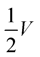 bias method (a) and bias method (a) and 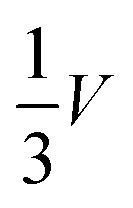 method (b). method (b). | ||
These bias schemes are effective ways to update and obtain states of the memristor crossbar array. However, for realization of efficient states update in situation where voltage pulses is messaged and complicated, such as spike neural network, and for a lower energy consumption, device level to suppress sneak path currents issue for precise resistance modulation of the array is necessary.
2. Solutions to the sneak path current issue
2.1 1T1M
The 1T1M cell structure is an effective solution to the sneak-path current issue. The 1T1M crossbar array is called the active crossbar array, where the series transistor plays the role of a switch. When the series field effect transistor is in the ON-state, it behaves much like a wire with high conductance. Consequently, the voltage can entirely drop across the memristor no matter the polarity of the biased voltage, which facilitates the state switching of the memristor. When the series field effect transistor is in the OFF-state, nearly no current flows through the cell and no voltage drops across the memristor. Via deliberately manipulating the ON–OFF state of transistors, precise selection of a designated memory cell can be realized.A typical schematic diagram of the 1T1M crossbar array is shown in Fig. 3. Here the line which activates memristors is called the bit line (B), and the gate line (G) controls the ON/OFF state of the cell. Bit-lines and gate-lines are usually perpendicular to each other. For example, when one control operation from A1 and B1 is implemented on M1 (gate-line 1 in the ON state), the other adjacent gate-lines are set to the OFF state to avoid crosstalk. Thus, the sneak path currents can be efficiently suppressed to enable accurate resistance programming and reading in the 1T1M crossbar array. The 1T1M has a cell area of 8F2, which is relatively large and limits the scaling of the array and integration density. To minimize as much as possible the scaling issue, a high channel conductance of transistors is preferred. On the other hand, CMOS transistors take advantage of their sophisticated fabrication techniques and scalability, whereby large 1T1M crossbar arrays could be easily achieved. Furthermore, by offering compliance currents, the gate lines in the 1T1M crossbar array assist in obtaining the linear and symmetric conductance increase and decrease with minimal cycle-to-cycle and device-to-device variations.13 This is favored by the time-efficient current domain VMM computing.
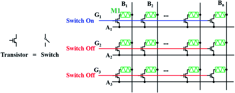 | ||
| Fig. 3 Schematic diagram of a 1T1M crossbar. | ||
Therefore, 1T1M crossbar arrays have already been widely studied.6,13–24 Wu's group fabricated a 128 × 8 1T1M crossbar array of TiN/TaOx/HfAlyOx/TiN devices.25 Using this 1024-cell array with parallel online training, a grey-scale face classification is demonstrated for the first time experimentally. The energy consumption is 1000 times less than that of the Intel Xeon Phi processor with off-chip memory and the accuracy on test sets is close to the result using a central processing unit. Xia and Yang's groups built up a 128 × 64 Ta/HfO2 1T1M crossbar array and used it for efficient analogue signal and image processing and other machine learning tasks.6,13,26,27 Based on the 1T1M crossbar array, they further demonstrated in situ training of feed-forward and recurrent convolutional memristor networks.28
Very recently, Wu's group demonstrated reliable and uniform analogue switching behaviors in the 2048 1T1M crossbar array of TiN/TaOx/HfOx/TiN devices.29 By integrating eight 2048-cell 1T1M crossbar arrays on a printed circuit board (PCB) and a field-programmable gate array evaluation board (ZC706, Xilinx), they successfully built a five-layer memristor-based CNN and performed MNIST image recognition with a high accuracy of more than 96 per cent. They demonstrated that the energy efficiency in memristor-based CNN neuromorphic systems is two orders of magnitude greater than that of the state-of-the-art graphics-processing units.29 Despite the slightly overshadowed scaling issue, the 1T1M crossbar arrays show great potential for neuromorphic application.
2.2 1D1M
The 1D1M crossbar array with a unit cell area of 4F2 is a promising architecture for high-density memory due to its excellent scalability. As shown in Fig. 4a, the 1D1M cell structure is composed of two elements: one diode and one memristor, and these two devices are connected in series. The current of a forward-biased diode is relatively large while the current is blocked when the diode is reverse-biased. By connecting a unipolar resistive switching device to this diode in series, this double-device structure displays a resistive switching behavior with a rectifying property.30 Consequently, this rectifying property can be used to inhibit sneak current, as implied by the red dashed line in Fig. 4a and b. In addition, the series diode also acts as an external load resistor to suppress the overflow current during the resistance transition, which significantly improves the cycle-to-cycle distribution of the integrated cells.30,31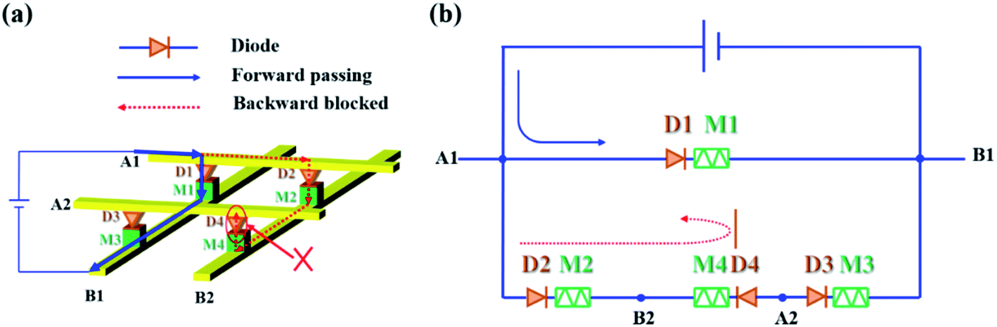 | ||
| Fig. 4 (a) A diagram and (b) equivalent circuit of a 2 × 2 crossbar array containing memory elements and diodes in series, in which the sneak path current is inhibited. | ||
Some requirements must be satisfied for a series diode in the passive crossbar array. A high rectification ratio, defined as the ratio between forward and reverse currents, is the most crucial one. A higher rectification ratio eliminates more sneak-path currents and allows larger passive crossbar arrays. Another performance concerned is the forward current density. Since the forward current should be high enough to switch the series memristor, a higher forward current density allows a smaller cell area of the diode and a higher integration density. Other factors such as endurance, a low temperature fabrication process and compatibility with CMOS technology are also considered when approaching their commercial application. Some recent advances of 1D1M structures, concerning parameters mentioned above, are summarized in Table 1.
| D | M | Current densitya | Fabrication temperature | Ratiob | Endurance | Retention | Current array size | Ref. |
|---|---|---|---|---|---|---|---|---|
| a The forward current density of the series diode. b The ratio is defined as the ratio between forward and reverse currents of the lowest resistance state of the 1D1M unit. | ||||||||
| Pt/TiO2/Ti Schottky | Ti/SiOx/Pt unipolar | 102 A cm−2 (2 V) | ≤200 °C | 105 (±2 V) | 300 (1D1M) | >105 s | 8 × 8 | 32 |
| Pt/TiO2/Ti Schottky | Pt/TiO2/Pt unipolar | >104 A cm−2 (2 V) | Near room temperature | 109 (±2 V) | 108 (D), 500 (1D1M) | 104 s | 4 × 4 × 2 (integrated 2 layer) | 33 |
| Pt/InZnOx/CuOx/Pt p–n junction | Pt/Ti-doped NiO/Pt unipolar | 104 A cm−2 (2 V) | Room temperature | 102 (±1 V) | 100 (1D1M) | — | 8 × 8 | 30 |
| Pt/n-type Si Schottky | Pt/Ta2O5/Pt unipolar | >106 A cm−2 (1 V) | — | 102 (±1 V) | 103 (1D1M) | 104 s | — | 31 |
| Pt/a-IGZO/Cu Schottky | Pt/HfO2/Cu bipolar | 102 A cm−2 (1 V) | Room temperature | 103 (±0.5 V) | 108 (D) | — | — | 34 |
| Ni/TiO2/Ti Schottky | Al/STN/Pt bipolar | 104 A cm−2 (1 V) | 100 °C | 103 (±0.5 V) | — | >105 s | — | 35 |
Yoon et al. reported a 1D1M crossbar memory array fabricated by physical vapor deposition methods at low temperature.32 The unit consists of a nanoporous SiOx film and a TiO2 oxide-based diode and shows uniform and stable memory performances even under mechanical deformation, while the endurance of 300 should be optimized. The low temperature fabrication process and flexible properties allow compatibility with not only conventional semiconductor processes, but also flexible memory applications. Using near-room-temperature physical vapor deposition methods, Kyung et al. fabricated 1D1M units with a TiO2-based Schottky diode and unipolar resistance switching TiO2.33 Based on these outstanding units whose rectification ratio is as high as 1.4 × 10⁹, they demonstrated a double-layer-stacked (4 × 4 × 2) 1D1M crossbar array, confirming the possible route for the multi-stacked memory structure.33
It is noted that the 1D1M method prefers unipolar memristors where the set and reset processes occur at the same voltage polarity, because the voltage mainly drops across the diode and hardly switches the resistance back in the bipolar one when the cell is reversely biased. Since the bipolar-type memory is more appropriate in most neural networks where resistance states are altered by simple voltage pulses with different voltage polarities, diodes satisfying bipolar memristors are required. This makes it necessary for the diode to meet at least two necessary requirements: (1) high forward current density and low reverse current density as in a regular diode to guarantee forward resistive switching and to suppress the sneak path currents. (2) Enough reverse current density at the voltage larger than the breakdown voltage (so called Zener voltage) to guarantee reverse resistive switching. When a forward voltage is applied to update resistance state of the intended memristor, only the middle cell in the sneak paths (D4M4 in Fig. 4) sustains an ultrahigh resistance state due to the reversed series diode and accommodates most of the applied voltage. To eliminate unintended programming, the amplitude of the reverse threshold voltage should be higher than the forward threshold voltage in the integrated one diode and one bipolar memristor unit. Despite some advances of bipolar 1D1M devices,34,35 the array application of 1D1M for bipolar memristors is still in its early stage.
2.3 1S1M
In a 1S1M array, a two-terminal selector device is connected to each memristor cell in series keeping the unit cell area of 4F2. The selector is actually a bidirectional highly nonlinear resistor. The selector and memristor can be stacked on top of each other, giving a higher density potential than the 1T1M scheme. As sketched in Fig. 5a and b, the I–V curve of the 1S1M structure shows very low current at half read (also program) voltage (high resistance), while the resistive switching of the memristor occurs in the high voltage region.36 The nonlinearity k of an I–V curve is defined as k = I(Vop)/I(Vop/2), where Vop is the operation voltage applied to the selected cell for reading or writing. As discussed in Part 1.3, during the programing/reading process in the 1S1M crossbar array, full voltage is only applied to selected cells, while half voltage is biased on these half-selected cells for the V/2 method and |V/3| is biased on half-selected and unselected cells for the V/3 method. Thus, the nonlinear property can effectively prevent the sneak effect in the 1S1M crossbar array. Consequently, the nonlinear I–V curve of the 1S1M unit can use the charge domain method when performing the VMM computing.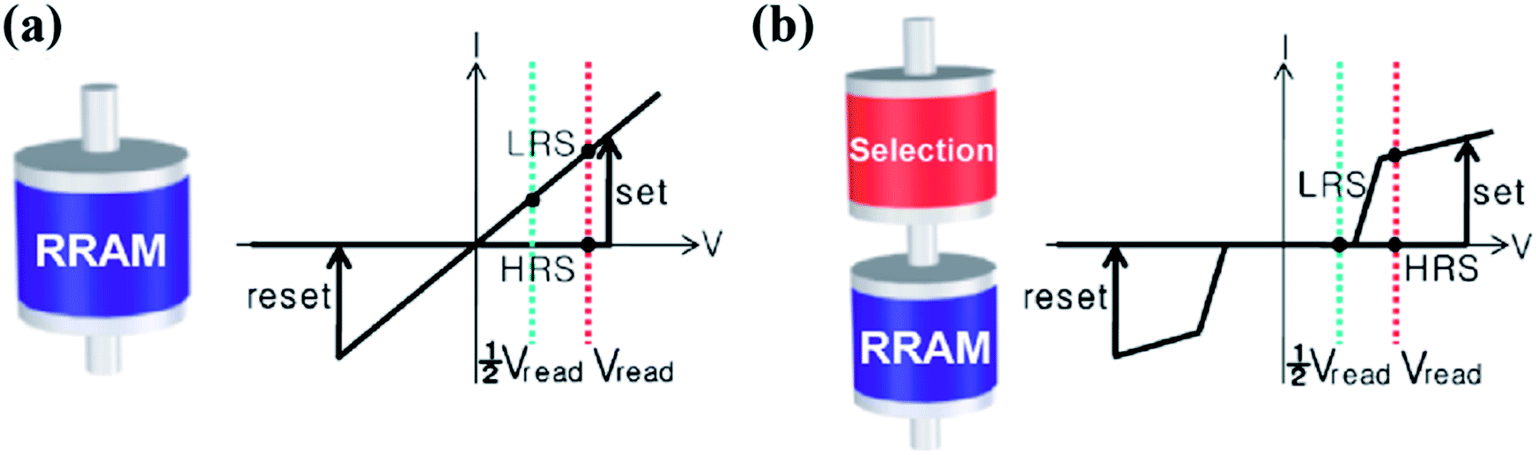 | ||
| Fig. 5 (a) Schematic diagram of the bipolar Resistive-RAM (RRAM) without a selection device (left), and the corresponding I–V model (right). (b) Schematic diagram of the bipolar RRAM with a selection device (left), and the corresponding I–V model (right) (reproduced from ref. 36, Copyright 2011, with permission of AIP Publishing). | ||
Similar to the requirements of a series diode in Part 2.2, high nonlinearity and large current density in the high voltage region benefit a large and dense crossbar array. The large current at high voltage is essential for the resistive switching of the series memristor, and a bigger nonlinearity of the I–V curve also results in higher resistance within the low voltage region, which benefits low energy consumption. Other factors such as endurance, a low temperature fabrication process and compatibility with CMOS technology are also considered when approaching their commercial application. Especially, the endurance of a selector should be significantly greater than that of its series memristor because the selector is turned on for every programming and reading event. The tunneling barrier37,38 and n–p–n39 or p–n–p40 junctions are commonly used in selectors. Ovonic threshold switching (OTS) behavior could also be used to achieve high nonlinearity for oxide capacitor devices; this requires the threshold resistive switching to occur transiently (less than 10 ns).41 Some recent advances of the 1S1M structure, concerning parameters mentioned above, are summarized in Table 2. The following are carefully picked examples, categorized by their intrinsic physical mechanisms, in which their merits, drawbacks and opportunities are discussed.
| S | M | Current densitya | Fabrication temperature | Nonlinearityb | Endurance of S | Dynamicsc | Ref. |
|---|---|---|---|---|---|---|---|
| a The highest current density of the series selector. b The nonlinearity is obtained from the selector. For the ovonic threshold switching (OTS) selectors, this value is obtained as selectivity (Rhigh/Rlow, ratio between resistances before and after threshold switching). c The switch speed for the transition (up) and delay (down) in these OTS selectors. | |||||||
| Pt/TaN1+x/Ta2O5/TaN1+x/Pt, tunneling barrier | Pt/TaN1+x/Pt | 103 A cm−2 | 400 °C | 104 | 108 | — | 38 |
| TaN/ITO/Co3O4/ITO/TaN, n–p–n | TaN/Al2O3/ZrO2/Al2O3/TaN | 6.5 A cm−2 | Room temperature | 103 | 107 | — | 39 |
| Pt/CoOx/IGZO/CoOx/Pt, p–n–p | Pt/TaOx/TiN | 0.1 A cm−2 | — | 104 | 104 | — | 40 |
| Ag/HfOx/Ag, OTS | Pd/Ta2O5/TaOx/Pd | >104 A cm−2 | 200 °C | 1010 | 108 | 75 ns, 300 ns | 42 |
| TiN/Nb1−xO2/Pt, OTS | Cu/HfO2/Pt | >106 A cm−2 | — | 102 | 1012 | <10 ns, <10 ns | 41 |
| W/SiTe/W, OTS | — | 107 A cm−2 | Room temperature | 105 | 108 | 2 ns, 7 ns | 43 |
| TiN/SiTe/Ag, OTS | — | >102 A cm−2 | 300 °C | 104 | 105 | 30 ns, 5.1 μs | 44 |
| TiN/GeSe/TiN, OTS | — | 103 A cm−2 | 300 °C | 107 | 105 | 100 ns, 300 ns | 45 |
| Ti/CuO-NW/Ti, OTS | — | — | — | 104 | 105 | — | 46 |
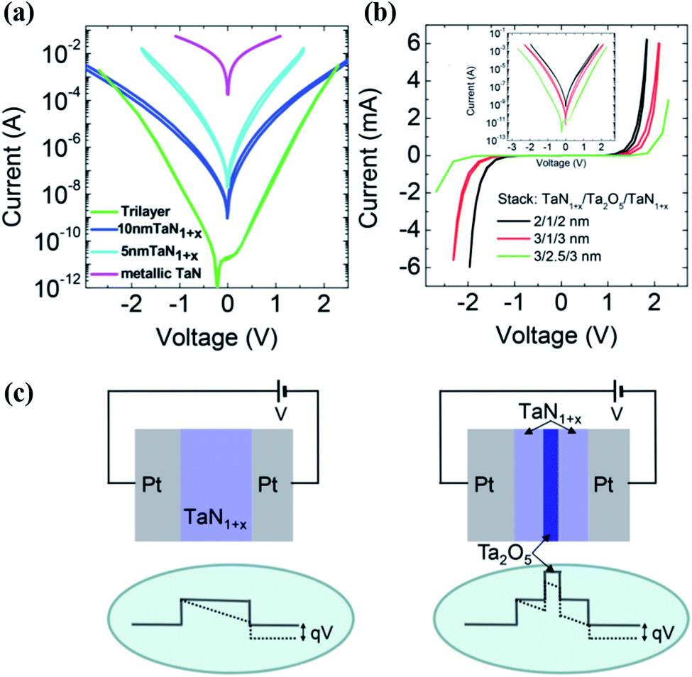 | ||
| Fig. 6 (a) I–V curves through metallic TaN and single TaN1+x layer barriers with two different thicknesses (5 and 10 nm) and trilayer (3 nm TaN1+x/2.5 nm Ta2O5/3 nm TaN1+x) barriers. (b) I–V curves through three trilayer devices with the thickness of each layer being 2/1/2, 3/1/3, and 3/2.5/3 nm. The inset is in the semilog plot. (c) Schematic band diagrams of the single and trilayer barrier structures (reproduced from ref. 38, Copyright 2015, with permission of John Wiley & Sons, Inc). | ||
Despite the merits of trilayer tunneling barriers, such as large nonlinearity and high endurance, tunnel selectors are promising due to the following reasons: the nonlinearity results from the intrinsic physical mechanisms, which are well understood and reproduced by accurate mathematical modeling. The intrinsic abrupt high currents don't need assistance of Joule heating, and are independent of temperature. These characteristics benefit low energy consumption and wide available temperature windows. Furthermore, tunnel selectors possess the advantages of intrinsic speed and reproducibility of their I–V curves. One of the challenges is that fabricating high-quality ultrathin films usually needs a high temperature process.47,48 High-quality tunnel selectors processed at room temperature, such as organic tunneling junctions,49 are under explored.
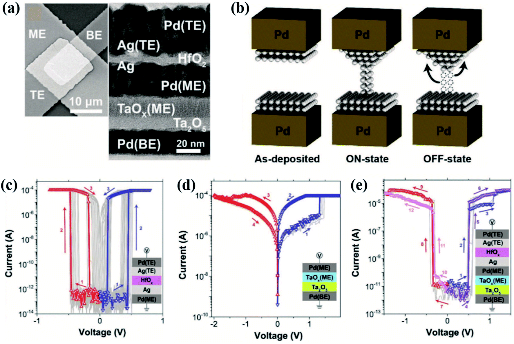 | ||
| Fig. 7 (a) Structure of the integrated 1S-1R device consisting of a Pd/Ta2O5/TaOx/Pd memristor and a Pd/Ag/HfOx/Ag/Pd selector highlighted by SEM and cross-sectional TEM techniques. (b) Schematic diagram of the filament during the threshold switching process. (c) Repeatable bidirectional threshold switching of the individual Pd/Ag/HfOx/Ag/Pd selector. (d) Repeatable bipolar resistive switching of the individual Pd/Ta2O5/TaOx/Pd memristor. (e) Repeatable nonlinear resistive switching of integration of the selector and memristor (reproduced from ref. 42, Copyright 2017, with permission of John Wiley & Sons, Inc). | ||
To improve the transition time, Lv and Liu's groups designed an ovonic threshold switching selector governed by the pure electron transition effect.41 In their Nb1−xO2 based selector, the threshold switching is triggered by local thermal runaway which reduces the energy barrier. There are no ions moving or phase transitions in the threshold switching process. Consequently, the speed of less than 10 ns and an ultra-high endurance of up to 1012 cycles are obtained, while the nonlinearity is 500, in this pure electron selector. Other pure electron OTS selectors based on SiTe with a transition of 2 ns and a delay of 7 ns are reported.43 Corresponding endurance and nonlinearity are 108 cycles and 105, respectively. The OTS selectors based on the pure electron mechanism provide a promising prospect for large and dense crossbar arrays.
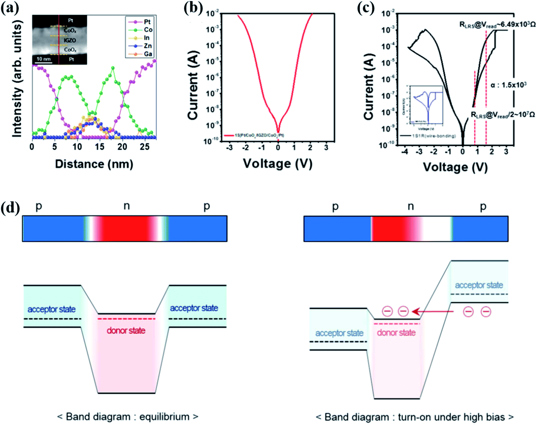 | ||
| Fig. 8 (a) High-resolution EDS (HR-EDS) elemental line profile across a line of the STEM image, where the inset shows a dark-field STEM image of the Pt/CoOx/IGZO/CoOx/Pt frame. (b and c) I–V curves of a CoOx/IGZO/CoOx selector (b) and electrical connection unit containing both the Pt/CoOx/IGZO/CoOx/Pt selector and Pt/TaOx/TiN memristor (c). (d) Schematic band diagram of the device p(emitter)–n(base)–p(collector) under zero (low) and high (above threshold) voltage bias, respectively (reproduced from ref. 40, Copyright 2015, with permission of Springer Nature). | ||
Similarly, a highly nonlinear n–p–n selector is also reported.39 One resistor device connecting the proposed n–p–n selector demonstrates a high nonlinearity of 103, excellent endurance of 107 cycles, fast switching speed (60 ns), and stable retention (104 s) at 100 °C.39 The successful operation of the p–n–p or n–p–n selector and one memristor with the 1S1R architecture contributes a new route for advancing crossbar arrays. One of the challenges is the low current density in the p–n–p and n–p–n structures, which hinders a high-density crossbar array.
3. Single-device memory cell structure
A single memristor device with either self-nonlinear or self-rectifying I–V characteristics could suppress the sneak path currents without other assistant cells in a crossbar array, and is a great improvement to simplify the memory cell, which reduces the cost, and benefits highly integrated crossbar arrays. By listing necessary parameters as in 1D1T and 1S1T structures, recent advances of these single-device memristors used in crossbar arrays are summarized in Table 3. The following is a careful introduction separated as self-selective memristors and self-rectifying memristors.| Structure | Mechanismsa | Fabrication temperature | Nonlinearity or ratiob | Endurance | Retention | Ref. |
|---|---|---|---|---|---|---|
| a The mechanism of self-nonlinear or self-rectifying memristors. b The nonlinearity is for self-selective memristors and the ratio is for self-rectifying memristors. | ||||||
| Pt/TiO2-NRs/FTO, self-selective | Interface phase transition | 350 °C | 10 | — | 103 s | 50 |
| W/WO3/WOx/W, self-selective | Tunneling barrier | 500 °C | 8.8 | — | 103 s | 51 |
| Pd/TaOx/HfO2/Pd, self-selective | Tunneling barrier | 300 °C | 103 | — | — | 52 |
| TiN/HfO2/TaOx/Ti, self-selective | Tunneling barrier | — | 102 | 107 | 104 s | 53 |
| TiN/HfO2/TiOx/Ru, self-selective | Tunneling barrier | — | 103 | 107 | 104 s | 54 |
| Au/h-BN/G/h-BN/Ag, self-selective | Volatile Ag filament | 120 °C | 1010 | 106 | 106 s | 55 |
| Pt/Ta2O5/HfO2−x/TiN, self-rectifying | Schottky barrier | 280 °C | 103 | 103 | 104 s | 56 |
| Pt/TiO2/HfO2−x/TiN, self-rectifying | Schottky barrier | 280 °C | 103 | 103 | 106 s | 57 |
| Pt/TaOy/NP TaOx/Ta, self-rectifying | Schottky barrier | — | 104 | 103 | 104 s | 58 |
| Pt/C/NbOx/TiN, self-rectifying | Asymmetric potential barrier | Room temperature | 106 | — | — | 59 |
| Pt/HfO2/n+-Si, self-rectifying | Asymmetric potential barrier | 300 °C | 105 | 103 | 104 s | 60 |
| Pt/NbOx/TiOy/NbOx/TiN, self-rectifying | Asymmetric potential barrier | 300 °C | 105 | 103 | 103 s | 61 |
| Al/Cu-pMSSQ/Al, self-rectifying | Asymmetric potential barrier | 160 °C | 102 | — | — | 62 |
| p-Si/SiO2/n-Si, self-rectifying | Asymmetric potential barrier | 400 °C | 105 | — | 105 s | 63 |
3.1 Self-selective memristors
Self-selective memristors exhibit self-nonlinear I–V characteristics as the overall feature of 1S1T. Recently, various self-selective devices have been realized. Most devices have a bi-layer structure, but based on different physical mechanisms. The following are some typical examples categorized by mechanisms.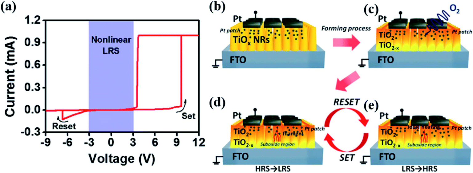 | ||
| Fig. 9 (a) Nonlinear I–V curves of the Pt/TiO2 NRs/FTO device. (b–e) Schematics of the nonlinear resistive switching mechanism. Four states: (b) the original state, (c) after the formation process, (d and e) back and forth switching between the set process and the reset process (reproduced from ref. 50, Copyright 2017, with permission of Springer Nature). | ||
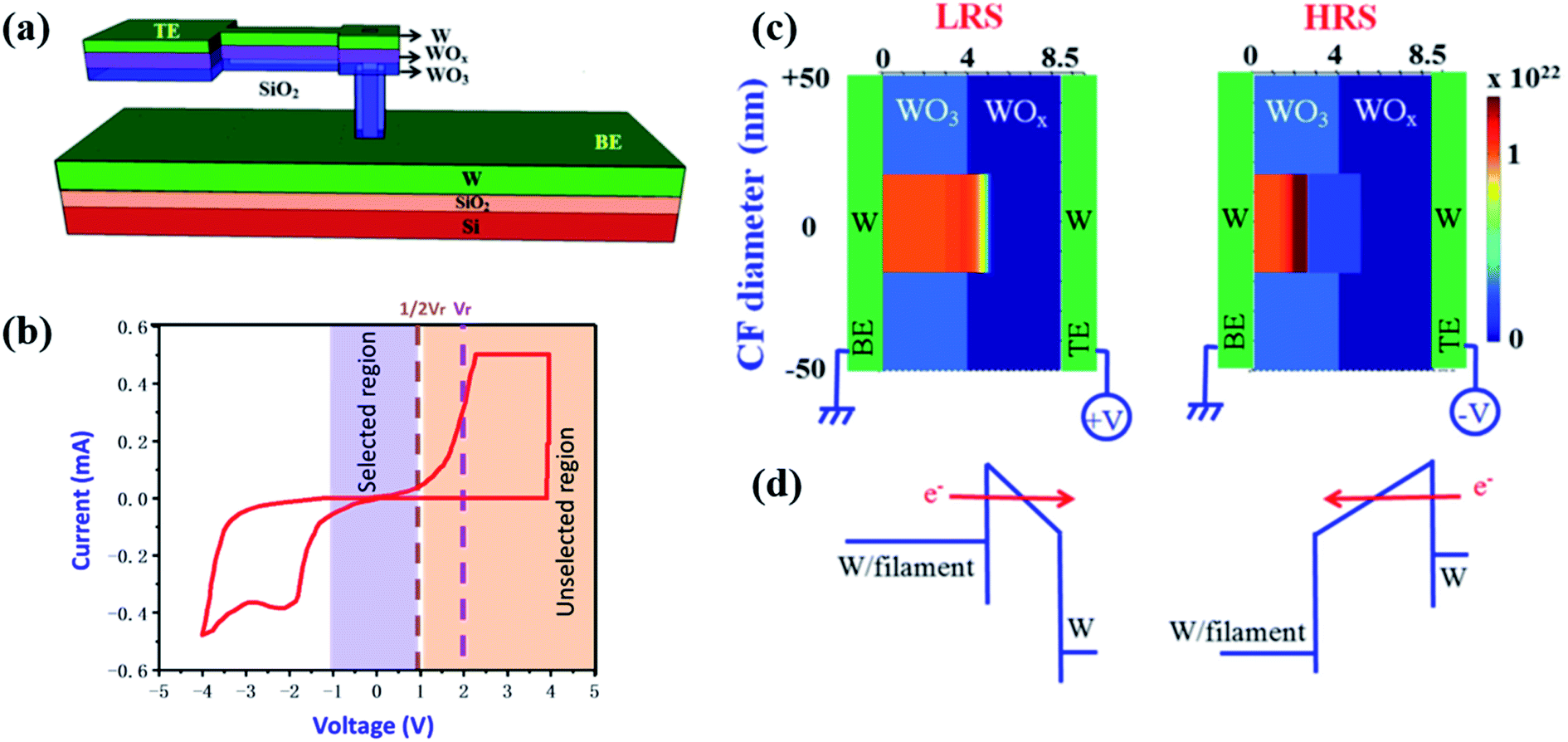 | ||
| Fig. 10 (a) Schematic diagram of a W/WO3/WOx/W resistive switching memory device. (b) I–V curves of the device. (c and d) Schematic diagram of the oxygen-vacancy filament of the device at both LRS and HRS (c) and the corresponding energy band diagram (d) (reproduced from ref. 51, Copyright 2016, with permission of Springer Nature). | ||
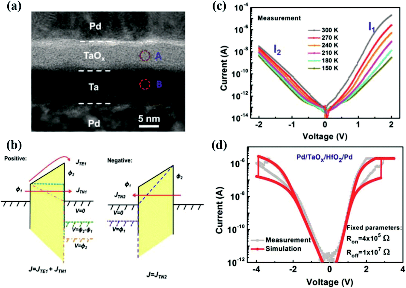 | ||
| Fig. 11 (a) The high resolution cross-sectional TEM image of a Pd/TaOx/Ta/Pd device. (b) Schematic diagrams of the band diagram of the Pd/TaOx/Ta/Pd tunneling junction under positive and negative bias. (c) I–V curves of the Pd/TaOx/Ta/Pd device at different temperatures from 150 K to 300 K. (d) I–V curves of the Pd/TaOx/HfO2/Pd device, the red lines represent the simulation using fixed values of Ron = 4 × 10⁵ Ω and Roff = 1 × 10⁷ Ω (reproduced from ref. 52, Copyright 2015, with permission of Royal Society of Chemistry). | ||
By designing a bilayer structure of HfO2/TaOx, where the HfO2 layer plays the role of the tunneling barrier53, Lv and Liu's groups realized self-selective resistive devices with outstanding properties, including high nonlinearity (>102) and high endurance (>107). Interestingly, based on these self-selective resistive devices, an 8-layer 3D vertical RRAM architecture with 5 nm size and 4 nm vertical pitch was demonstrated. Bayat et al. designed a Pt/Al2O3/TiO2−x/Ti/Pt memristor whose nonlinearity arises from the alumina tunneling barrier.66 Passive 20 × 20 crossbar arrays based on this nonlinear memristor were fabricated, in which leakage currents are sufficiently suppressed. Assisted by ex situ training, these passive 20 × 20 crossbar arrays achieve classification fidelity within 3% of that obtained in simulations66.
 | ||
| Fig. 12 (a) Schematic of the Au/h-BN/G/h-BN/Ag van der Waals heterostructure in the crossbar array architecture. (b) I–V curves of an Au/h-BN/G/h-BN/Ag memory cell in the crossbar array. (c) Schematic pictures of the Au/h-BN/G/h-BN/Ag memory cell for the four states in (b). States “1” and “3” represent the high-resistance state and low-resistance state of unselected cells, respectively. States “2” and “4” represent the high-resistance state and low-resistance state of a selected memory cell, respectively. A complete conductive silver filament is formed in state “2” and state “4”. A complete conductive boron vacancy filament is formed in state “3” and state “4”. The gray, purple, blue, yellow and white spheres represent silver, hexagonal boron nitride, graphene, gold and boron vacancies, respectively (reproduced from ref. 55, Copyright 2019, with permission of Springer Nature). | ||
3.2 Self-rectifying memristor
In contrast to selector-less memristors whose I–V curves are nonlinear, self-rectifying memristors are single-stack devices where reverse current is extremely small. Therefore, self-rectifying memristors resemble bipolar 1D1M structures. Thus, as discussed in Part 2.2, to eliminate the unintended programming, the amplitude of the reverse threshold voltage should be higher than that of the forward threshold voltage in self-rectifying memristors. The self-rectifying property mostly originates from the asymmetric barrier due to the Schottky contact or asymmetric potential in the devices, while various mechanisms contribute to these memristive behaviors. The following are some typical examples.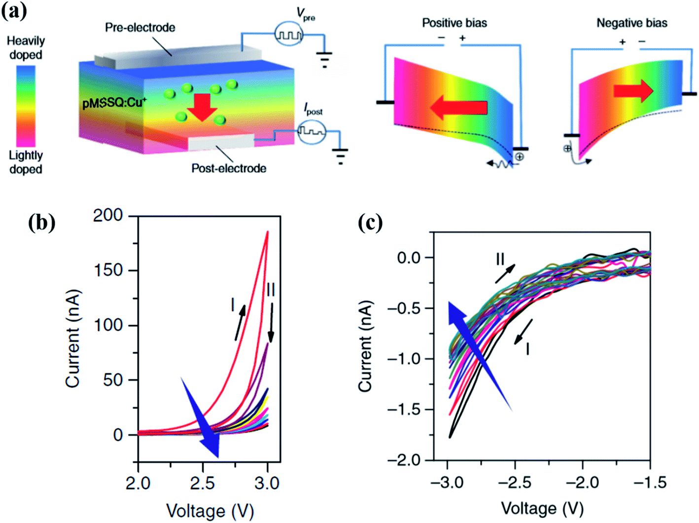 | ||
| Fig. 13 (a) Schematic diagram and band structure of the sandwiched structure of Al (bottom electrode)/lightly doped layer/highly doped layer/Al (top electrode), and the kinetic model of carrier transportation under both polarization of voltage bias. (b) I–V curves under consecutive positive bias sweeps. (c) I–V curves under consecutive positive bias sweeps after the positive bias sweeps (reproduced from ref. 62, Copyright 2017, with permission of Springer Nature). | ||
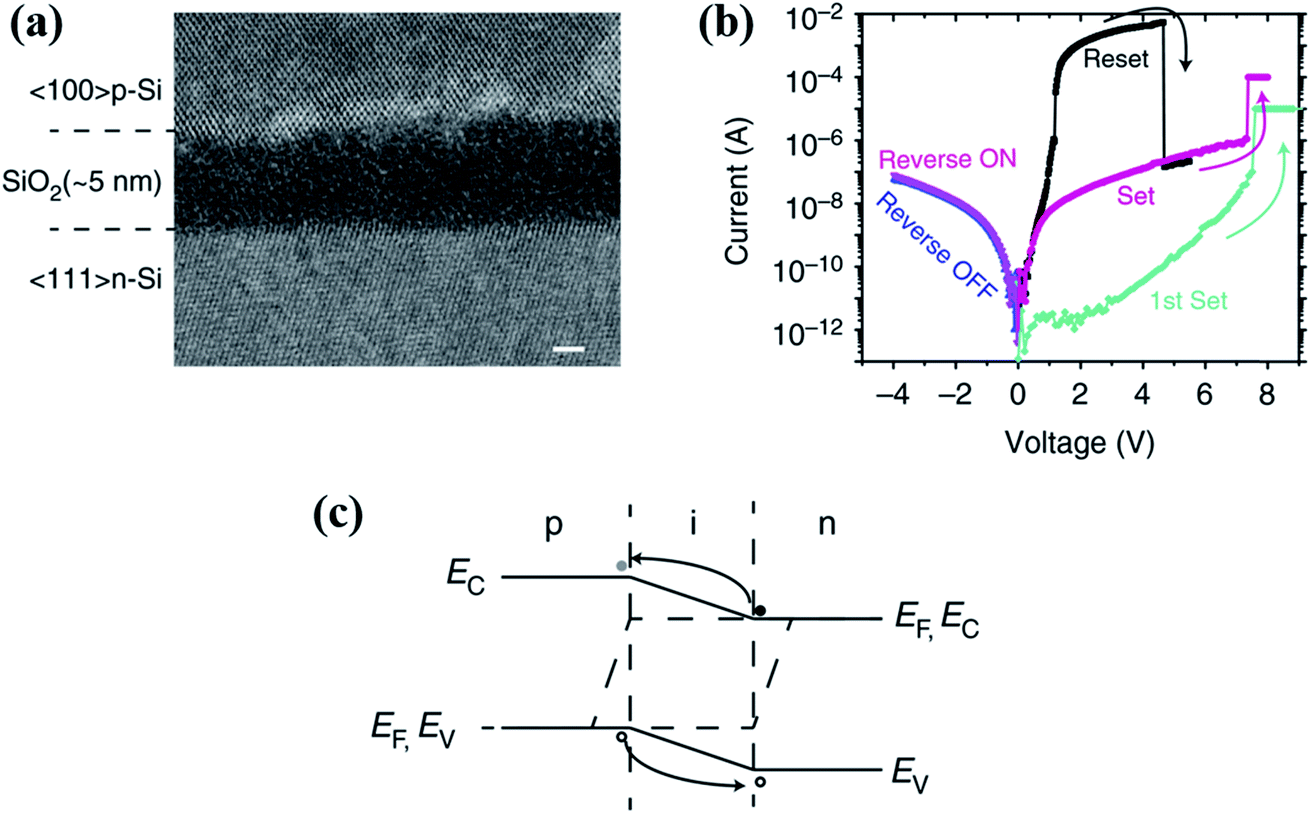 | ||
| Fig. 14 (a) Cross-sectional TEM image of the Si/SiO2/Si device shows a single crystalline structure for the top and bottom electrodes and the 5 nm amorphous SiO2 switching layer. Scale bar, 2 nm. (b) A typical unipolar resistive switching I–V curve of the Si/SiO2/Si device. The n-Si bottom electrode was grounded while the bias was applied to the p-Si top electrode. (c) The band diagram in LRS under a forward bias describes a piece of non-degenerated silicon bridge between two degenerate silicon electrodes. The excess holes flow from the p-type electrode to the n-type electrode while the electrons flow from the n-type electrode to the p-type electrode (reproduced from ref. 63, Copyright 2017, with permission of Nature Publishing Group). | ||
Kim et al. designed a low-current and self-rectifying Pt/NbOx/TiOy/NbOx/TiN device61 (Fig. 15a), where the memristive behavior is attributed to the electron trapping/detrapping process while the asymmetric potential barriers induce a self-rectifying ratio of ∼105. The schematic energy band diagram of the device is shown in Fig. 15b; a trap energy as deep as 0.8 eV is formed in the TiOy layer. The as-deposited devices experienced a 300 °C atmosphere during the fabrication process, which facilitates the trap sites to be filled with electrons. The I–V curves are shown in Fig. 15a, and the corresponding evolution of energy diagrams is shown in Fig. 15c. As mentioned above, electrons are trapped in the trap sites initially. These electrons attract positive charges to accumulate at the interface of the electrodes, leading to a built-in electric field pointing toward the trap sites. Under this circumstance, the whole barrier height increases, giving a high resistive state (HRS). When positively biased voltage is applied, the Fermi level of the Pt electrode is pulled down, and electrons are released to the Pt electrode. This detrapping process leads the device to the low resistive state (LRS). There can also be a trapping process from the TiN electrode to the trap sites, which is much weaker than the detrapping process because of the longer tunneling distance between the TiN and trap sites. Similarly, the memristor is switched back to the HRS when the negatively biased voltage sweeps.
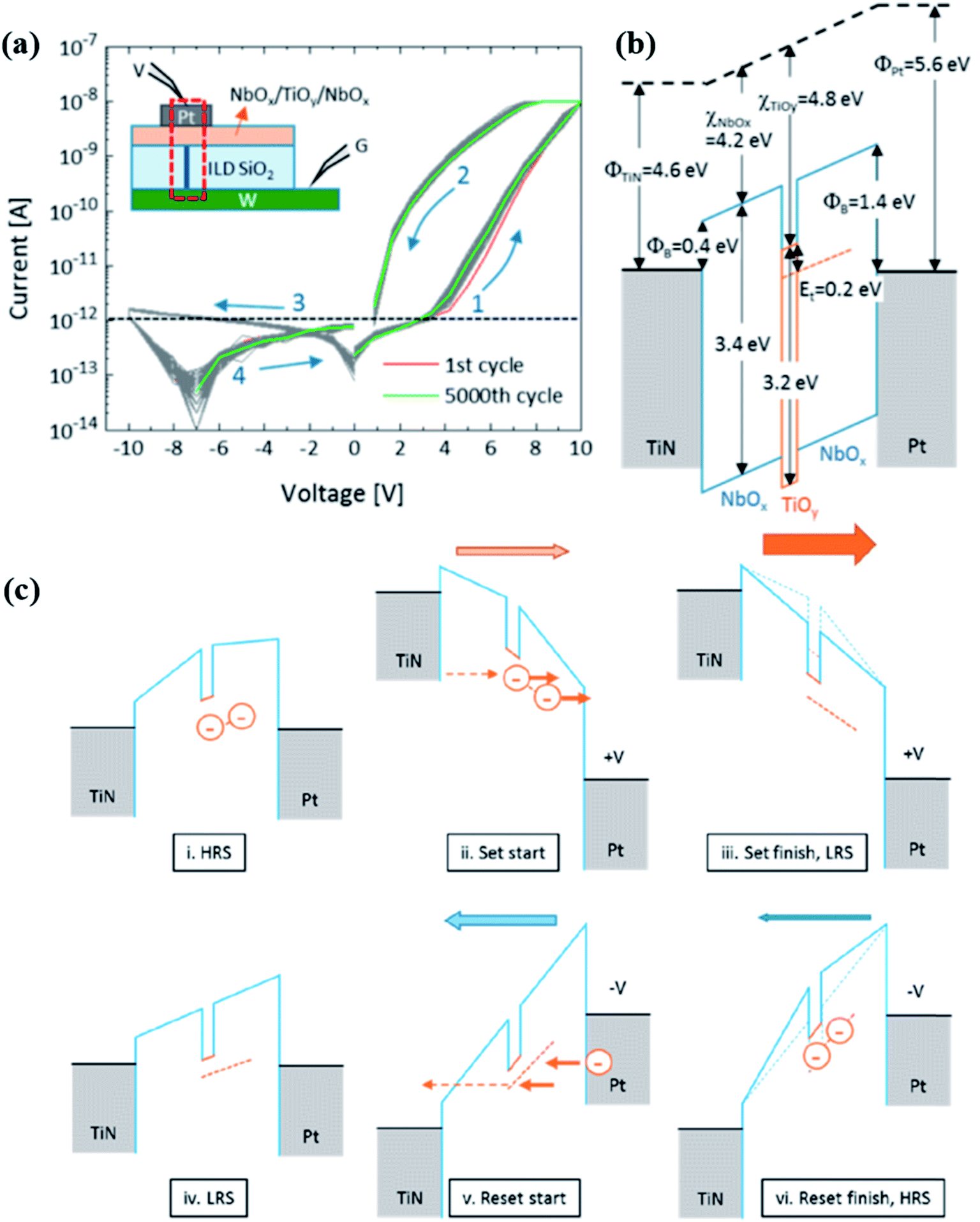 | ||
| Fig. 15 (a) I–V curves of the Pt/NbOx/TiOy/NbOx/TiN device. Inset shows the structure of the device and the test setup for the measurement. (b) The energy band diagram of the device. (c) Diagram of the charge capture and decapture process in the device. (i) The HRS, electrons fill the trap sites. (ii and iii) A positive set bias is applied on the Pt electrode, (iv) LRS, the trapped electrons can be released. (v and vi) A negative reset bias is applied, and the HRS is restored (adapted from ref. 61, Copyright 2016, with permission of American Chemical Society). | ||
Wang et al. designed a synaptic memory of Pt/C/NbOx/TiN.59 The charge trapping and detrapping in the NbOx film dominate the resistive switching. The inserted C layer plays a role of forming an asymmetric potential barrier in the device, resulting in a self-rectifying ratio of 106. The high self-rectifying ratio of 106 effectively eliminates sneak path currents, and thus the conductance in a crossbar array can be efficiently programed. Excellent classification accuracy (95.7%) of handwritten digits is achieved by a simulation of two-layer perceptron neural networks based on these self-rectifying Pt/C/NbOx/TiN devices.
There are also other self-rectifying memristors associating memristive mechanisms such as interaction of composition dependent thermal conductivity and oxygen-ion migration,58,68–70 electron tunneling controlled by ferroelectric surfaces,71,72 and interfacial trap site engineering.73 Most reported self-rectifying memristors do not show an abrupt increase and decrease of conductance. These properties indicate that self-rectifying memristors have great potential application for neuromorphic networks. However, most reported self-rectifying memristors suffer from an important issue of poor endurance (Table 3). This may be due to the fact that a high barrier is usually induced to achieve self-rectification, which inevitably needs a higher voltage operation for programing the states. Reducing the syndrome of high voltage needs to be explored.
4. Perspectives
Memristors are new non-volatile electronic memory devices with programmable resistance that has enormous potential application in tomorrow's electronics. One of the appealing aspects is that memristor crossbar arrays can be an ideal candidate for hardware neuromorphic networks. The memristor crossbar array can implement algorithms more efficiently with much lower power consumption. However, to realize this attractive prospect, the sneak-path current issue must be overcome. Thanks to the efforts of researchers in the academic domain over the years, quite a number of solutions have been proposed to solve this sneak-path problem, and each specific category of solutions has been developed at a more and more sophisticated level, which improves the possibility for real applications.As a matter of fact, a potential solution is the 1T1M structure. Due to its high compatibility with the CMOS process, 1T1M has become the most practical approach. The transistor in this structure could precisely manipulate the ON/OFF state of the cell, which mitigates the sneak path currents and half-select issues during array programming and reading. Moreover, the gate voltage could provide controllability of the synaptic weight by regulating the limit resistance of the cell, which is significant for application in neuromorphic networks, such as, by offering compliance currents, the gate lines in the 1T1M crossbar array assist in obtaining the linear and symmetric conductance increase and decrease with minimal cycle-to-cycle and device-to-device variations, which is favorable for time-efficient current domain VMM computing.
However, 1T1M has a cell area of 8F2, which is relatively large and limits the scaling of the array and integration density. To minimize as much as possible the scaling issue, a high channel conductance of transistors is preferred. Despite the large cell area, CMOS transistors take advantage of their sophisticated fabrication techniques and scalability, whereby vast 1T1M crossbar arrays are fabricated and demonstrated to perform well in various complicated information processing operations.
In a passive array, which has a cell area of 4F2, a much higher packing density and 3D stackability are achieved. On the other hand, it suffers from half-select issues, resulting in large energy consumption during the programming and reading of the cells in large-scale arrays. To overcome this issue, a high rectification ratio or nonlinearity must be induced to memristors by connecting a series diode or nonlinear selector or by itself. The series diode or nonlinear selector doesn't increase footpoints, thus sustaining the advantage of high packing density and stackability.
For the 1D1M structure, a higher rectification ratio and bigger forward current density allow larger and denser crossbar arrays. The series diode also acts as an external load resistor to suppress the overflow current during the resistance transition, which significantly improves the cycle-to-cycle distribution of the integrated cells. Recently, the forward/reverse ratio of the series diode has been continuously increased. The application of this solution is not only subject to unipolar memristors but extends to bipolar devices. The TiO2-based Schottky diode with a rectification ratio as high as 1.4 × 10⁹ and an endurance of 108 cycles is very promising for application in large crossbar arrays.
As for 1S1M, to reduce the energy consumption and improve the performance of programming and reading of the cells in large-scale arrays, selector devices with high nonlinearity must be created. Nonlinear selectors based on the tunneling barrier, OTS and p-/n-combination have been vastly researched in these 3 years. The nonlinearity of tunneling barrier selectors results from the intrinsic physical mechanism. The abrupt high currents don't need assistance of Joule heating, and are independent of temperature, which benefits low energy consumption and wide available temperature windows. The tunnel selectors also possess excellent speed and reproducibility. One of the drawbacks is the high temperature fabrication process, limiting its further integrating. Low temperature tunneling barrier selectors need to be explored. The biggest stumbling block for p–n–p and n–p–n selectors is the low current density, which needs a large cell area to switch the accompanied memristor and hinders a high-density crossbar array. The outstanding nonlinearity and endurance behaviors in ion-based OTS selectors are appealing. But the dynamics of ions is slower compared with electrons; electron-based OTS selectors usually possess a transition time less than 10 ns, and are also capable of high endurance, such as an ultrahigh endurance of 1012 in Nb1−xO2 based and 108 in SiTe based selectors. OTS selectors based on the pure electron mechanism are promising for large and dense crossbar arrays.
Self-selective and self-rectifying memristors show great potential for solving the sneak-path current issue with a simple structure. These two aforementioned solutions using a single device instead of two move a step further in down-scaling (including the cost). Self-rectifying memristors usually suffer from poor endurance due to the high voltage operation. Self-nonlinear selectors based on either CMOS-compatible oxides or van der Waals Materials are promising for huge and dense crossbar arrays. One note is recalled that VMM computation in 1S1M or single-device memristor crossbar arrays is limited to the charge domain method (by modulating the pulse width or number) due to the nonlinear I–V curves.
In short, this fast-growing field of research is still in its infancy and we hope this overview concerning the sneak-path current problem will benefit the field and arouse the curiosity and inventiveness of researchers and engineers from chemistry, physics, materials science, electronics and computing science.
Conflicts of interest
There are no conflicts to declare.Acknowledgements
This work was financially supported by the National Natural Science Foundation of China (61804055), the “Chenguang Program” supported by the Shanghai Education Development Foundation and the Shanghai Municipal Education Commission (17CG24), the Postdoctoral Science Foundation of China (2017M611501), the Shanghai Science and Technology Innovation Action Plan (19JC1416700), and the Shanghai Sailing Program (17YF1404200).Notes and references
- G. W. Burr, R. M. Shelby, A. Sebastian, S. Kim, S. Kim, S. Sidler, K. Virwani, M. Ishii, P. Narayanan, A. Fumarola, L. L. Sanches, I. Boybat, M. Le Gallo, K. Moon, J. Woo, H. Hwang and Y. Leblebici, Adv. Phys.: X, 2016, 2, 89–124 Search PubMed.
- B. Hudec, C.-W. Hsu, I. T. Wang, W.-L. Lai, C.-C. Chang, T. Wang, K. Fröhlich, C.-H. Ho, C.-H. Lin and T.-H. Hou, Sci. China Inf. Sci., 2016, 59, 061403 CrossRef.
- S. Gi, I. Yeo, M. Chu, S. Kim and B. Lee, International SoC Design Conference (ISOCC), 2015, p. 215 Search PubMed.
- F. Pan, S. Gao, C. Chen, C. Song and F. Zeng, Mater. Sci. Eng., R, 2014, 83, 1–59 CrossRef.
- J. Y. Seok, S. J. Song, J. H. Yoon, K. J. Yoon, T. H. Park, D. E. Kwon, H. Lim, G. H. Kim, D. S. Jeong and C. S. Hwang, Adv. Funct. Mater., 2014, 24, 5316–5339 CrossRef CAS.
- M. Hu, C. E. Graves, C. Li, Y. Li, N. Ge, E. Montgomery, N. Davila, H. Jiang, R. S. Williams, J. J. Yang, Q. Xia and J. P. Strachan, Adv. Mater., 2018, 30, 1705914 CrossRef PubMed.
- F. Cai, J. M. Correll, S. H. Lee, Y. Lim, V. Bothra, Z. Zhang, M. P. Flynn and W. D. Lu, Nat. Electron., 2019, 2, 290–299 CrossRef CAS.
- H. Jiang, K. Yamada, Z. Ren, T. Kwok, F. Luo, Q. Yang, X. Zhang, J. J. Yang, Q. Xia, Y. Chen, H. Li, Q. Wu and M. Barnell, IEEE International Symposium on Circuits and Systems (ISCAS), 2018 Search PubMed.
- Q. Xia and J. J. Yang, Nat. Mater., 2019, 18, 309–323 CrossRef CAS PubMed.
- Y. Chen, G.-Y. Jung, D. A. A. Ohlberg, X. Li, D. R. Stewart, J. O. Jeppesen, K. A. Nielsen, J. F. Stoddart and R. S. Williams, Nanotechnology, 2003, 14, 462–468 CrossRef CAS.
- Y.-C. Chen, C. F. Chen, C. T. Chen, J. Y. Yu, S. Wu, S. L. Lung, R. Liu and C.-Y. Lu, IEEE International Electron Devices Meeting (IEDM), 2003, vol. 03, p. 905 Search PubMed.
- A. Ciprut and E. G. Friedman, IEEE Transactions on Very Large Scale Integration (VLSI) Systems, 2018, 26, 711–719 Search PubMed.
- C. Li, D. Belkin, Y. Li, P. Yan, M. Hu, N. Ge, H. Jiang, E. Montgomery, P. Lin, Z. Wang, W. Song, J. P. Strachan, M. Barnell, Q. Wu, R. S. Williams, J. J. Yang and Q. Xia, Nat. Commun., 2018, 9, 2385 CrossRef PubMed.
- S. Yu, Z. Li, P.-Y. Chen, H. Wu, B. Gao, D. Wang, W. Wu and H. Qian, IEEE International Electron Devices Meeting (IEDM), 2016, vol. 16, p. 416 Search PubMed.
- R. Mochida, K. Kouno, Y. Hayata, M. Nakayama, T. Ono, H. Suwa, R. Yasuhara, K. Katayama, T. Mikawa and Y. Gohou, Symposium on VLSI Technology Digest of Technical Papers, 2018, p. 175 Search PubMed.
- S. Ambrogio, P. Narayanan, H. Tsai, R. M. Shelby, I. Boybat, C. di Nolfo, S. Sidler, M. Giordano, M. Bodini, N. C. P. Farinha, B. Killeen, C. Cheng, Y. Jaoudi and G. W. Burr, Nature, 2018, 558, 60–67 CrossRef CAS PubMed.
- Y. Shi, L. Nguyen, S. Oh, X. Liu, F. Koushan, J. R. Jameson and D. Kuzum, Nat. Commun., 2018, 9, 5312 CrossRef CAS PubMed.
- C.-X. Xue, W.-H. Chen, J.-S. Liu, J.-F. Li, W.-Y. Lin, W.-E. Lin, J.-H. Wang, W.-C. Wei, T.-W. Chang, T.-C. Chang, T.-Y. Huang, H.-Y. Kao, S.-Y. Wei, Y.-C. Chiu, C.-Y. Lee, C.-C. Lo, Y.-C. King, C.-J. Lin, R.-S. Liu, C.-C. Hsieh, K.-T. Tang and M.-F. Chang, IEEE International Solid-State Circuits Conference (ISSCC), 2019, vol. 24.1, p. 388 Search PubMed.
- Y. Zhou, H. Wu, B. Gao, W. Wu, Y. Xi, P. Yao, S. Zhang, Q. Zhang and H. Qian, Adv. Funct. Mater., 2019, 29, 1900155 CrossRef.
- H. Tsai, S. Ambrogio, C. Mackin, P. Narayanan, R. M. Shelby, K. Rocki, A. Chen and G. W. Burr, Symposium on VLSI Technology Digest of Technical Papers, 2019, vol. T82 Search PubMed.
- C.-H. Wang, C. McClellan, Y. Shi, X. Zheng, V. Chen, M. Lanza, E. Pop and H.-S. P. Wong, IEEE International Electron Devices Meeting (IEDM), 2018, vol. 18, p. 528 Search PubMed.
- Y. Zhang, Z. Zhou, P. Huang, M. Fan, R. Han, W. Shen, L. Liu, X. Liu and J. Kang, Silicon Nanoelectronics Workshop (SNW), 2019 Search PubMed.
- C. Mohan, L. A. Camuñas-Mesa, E. Vianello, L. Periniolla, C. Reita, J. M. de la Rosa, T. Serrano-Gotarredona and B. Linares-Barranco, Microelectron. Eng., 2018, 198, 35–47 CrossRef CAS.
- H.-X. Zheng, Y.-C. Zhang, X.-H. Ma, Y. Hao, S. M. Sze, M.-C. Chen, T.-C. Chang, Y.-T. Su, W.-C. Chen, W.-C. Huang, P.-Y. Wu, Y.-F. Tan and Y.-L. Xu, IEEE Trans. Electron Devices, 2019, 66, 4706–4709 Search PubMed.
- P. Yao, H. Wu, B. Gao, S. B. Eryilmaz, X. Huang, W. Zhang, Q. Zhang, N. Deng, L. Shi, H. P. Wong and H. Qian, Nat. Commun., 2017, 8, 15199 CrossRef CAS PubMed.
- C. Li, M. Hu, Y. Li, H. Jiang, N. Ge, E. Montgomery, J. Zhang, W. Song, N. Dávila, C. E. Graves, Z. Li, J. P. Strachan, P. Lin, Z. Wang, M. Barnell, Q. Wu, R. S. Williams, J. J. Yang and Q. Xia, Nat. Electron., 2017, 1, 52–59 CrossRef.
- C. Li, Z. Wang, M. Rao, D. Belkin, W. Song, H. Jiang, P. Yan, Y. Li, P. Lin, M. Hu, N. Ge, J. P. Strachan, M. Barnell, Q. Wu, R. S. Williams, J. J. Yang and Q. Xia, Nature Machine Intelligence, 2019, 1, 49–57 CrossRef.
- Z. Wang, C. Li, P. Lin, M. Rao, Y. Nie, W. Song, Q. Qiu, Y. Li, P. Yan, J. P. Strachan, N. Ge, N. McDonald, Q. Wu, M. Hu, H. Wu, R. S. Williams, Q. Xia and J. J. Yang, Nature Machine Intelligence, 2019, 1, 434–442 CrossRef.
- P. Yao, H. Wu, B. Gao, J. Tang, Q. Zhang, W. Zhang, J. J. Yang and H. Qian, Nature, 2020, 577, 641–646 CrossRef CAS PubMed.
- M. Song, H. Lee, D. H. Seo, H.-J. Lee, J.-S. Kim, H.-S. Cho, H.-K. Lyu, S. Seo and M.-J. Lee, IEEE J. Electron Devices Soc., 2018, 6, 905–909 CAS.
- D. K. Lee, G. H. Kim, H. Sohn and M. K. Yang, Appl. Phys. Lett., 2019, 115, 263502 CrossRef.
- J. Yoon, Y. Ji, S.-K. Lee, J. Hyon and J. M. Tour, Adv. Electron. Mater., 2018, 4, 1700665 CrossRef.
- K. J. Yoon, G. H. Kim, S. Yoo, W. Bae, J. H. Yoon, T. H. Park, D. E. Kwon, Y. J. Kwon, H. J. Kim, Y. M. Kim and C. S. Hwang, Adv. Electron. Mater., 2017, 3, 1700152 CrossRef.
- Q. Wu, G. Yang, C. Lu, G. Xu, J. Wang, B. Dang, Y. Gong, X. Shi, X. Chuai, N. Lu, D. Geng, H. Wang, L. Li and M. Liu, IEEE Trans. Electron Devices, 2019, 66, 9 Search PubMed.
- K.-J. Lee, Y.-C. Chang, C.-J. Lee and Y.-H. Wang, Vacuum, 2017, 140, 35–41 CrossRef CAS.
- J. Shin, I. Kim, K. P. Biju, M. Jo, J. Park, J. Lee, S. Jung, W. Lee, S. Kim, S. Park and H. Hwang, J. Appl. Phys., 2011, 109, 033712 CrossRef.
- M. Wang, X. Lian, Y. Pan, J. Zeng, C. Wang, E. Liu, B. Wang, J. J. Yang, F. Miao and D. Xing, Appl. Phys. A: Mater. Sci. Process., 2015, 120, 403–407 CrossRef CAS.
- B. J. Choi, J. Zhang, K. Norris, G. Gibson, K. M. Kim, W. Jackson, M. X. Zhang, Z. Li, J. J. Yang and R. S. Williams, Adv. Mater., 2016, 28, 356–362 CrossRef CAS PubMed.
- D. Kumar, R. Aluguri, U. Chand and T.-Y. Tseng, IEEE Trans. Electron Devices, 2019, 66, 1296–1301 CAS.
- Y. C. Bae, A. R. Lee, G. H. Baek, J. B. Chung, T. Y. Kim, J. G. Park and J. P. Hong, Sci. Rep., 2015, 5, 13362 CrossRef CAS PubMed.
- Q. Luo, J. Yu, X. Zhang, K.-H. Xue, J.-H. Yuan, Y. Cheng, T. Gong, H. Lv, X. Xu, P. Yuan, J. Yin, L. Tai, S. Long, Q. Liu, X. Miao, J. Li and M. Liu, Symposium on VLSI Technology Digest of Technical Papers, 2019, vol. T236 Search PubMed.
- R. Midya, Z. Wang, J. Zhang, S. E. Savel'ev, C. Li, M. Rao, M. H. Jang, S. Joshi, H. Jiang, P. Lin, K. Norris, N. Ge, Q. Wu, M. Barnell, Z. Li, H. L. Xin, R. S. Williams, Q. Xia and J. J. Yang, Adv. Mater., 2017, 29, 1604457 CrossRef PubMed.
- Y. Koo, S. Lee, S. Park, M. Yang and H. Hwang, IEEE Electron Device Lett., 2017, 38, 568–571 CAS.
- B. Song, H. Xu, S. Liu, H. Liu and Q. Li, IEEE J. Electron Devices Soc., 2018, 6, 674–679 CAS.
- B. Song, H. Xu, S. Liu, H. Liu, Q. Liu and Q. Li, Appl. Phys. A: Mater. Sci. Process., 2019, 125, 772 CrossRef.
- C.-H. Huang, K. Matsuzaki and K. Nomura, Appl. Phys. Lett., 2020, 116, 023503 CrossRef.
- A. Chanthbouala, V. Garcia, R. O. Cherifi, K. Bouzehouane, S. Fusil, X. Moya, S. Xavier, H. Yamada, C. Deranlot, N. D. Mathur, M. Bibes, A. Barthelemy and J. Grollier, Nat. Mater., 2012, 11, 860–864 CrossRef CAS PubMed.
- W. Huang, Y. W. Fang, Y. Yin, B. Tian, W. Zhao, C. Hou, C. Ma, Q. Li, E. Y. Tsymbal, C. G. Duan and X. Li, ACS Appl. Mater. Interfaces, 2018, 10, 5649–5656 CrossRef CAS PubMed.
- B. B. Tian, J. L. Wang, S. Fusil, Y. Liu, X. L. Zhao, S. Sun, H. Shen, T. Lin, J. L. Sun, C. G. Duan, M. Bibes, A. Barthelemy, B. Dkhil, V. Garcia, X. J. Meng and J. H. Chu, Nat. Commun., 2016, 7, 11502 CrossRef CAS PubMed.
- C. H. Huang, T. S. Chou, J. S. Huang, S. M. Lin and Y. L. Chueh, Sci. Rep., 2017, 7, 2066 CrossRef PubMed.
- S. Chakrabarti, S. Samanta, S. Maikap, S. Z. Rahaman and H. M. Cheng, Nanoscale Res. Lett., 2016, 11, 389 CrossRef PubMed.
- M. Wang, J. Zhou, Y. Yang, S. Gaba, M. Liu and W. D. Lu, Nanoscale, 2015, 7, 4964–4970 RSC.
- Q. Luo, X. Xu, T. Gong, H. Lv, D. Dong, H. Ma, P. Yuan, J. Gao, J. Liu, Z. Yu, J. Li, S. Long, Q. Liu and M. Liu, IEEE International Electron Devices Meeting (IEDM), 2017, vol. 17, p. 48 Search PubMed.
- X. Xu, Q. Luo, T. Gong, H. Lv, S. Long, Q. Liu, S. S. Chung, J. Li and M. Liu, Symposium on VLSI Technology Digest of Technical Papers, 2016 Search PubMed.
- L. Sun, Y. Zhang, G. Han, G. Hwang, J. Jiang, B. Joo, K. Watanabe, T. Taniguchi, Y. M. Kim, W. J. Yu, B. S. Kong, R. Zhao and H. Yang, Nat. Commun., 2019, 10, 3161 CrossRef PubMed.
- J. H. Yoon, S. Yoo, S. J. Song, K. J. Yoon, D. E. Kwon, Y. J. Kwon, T. H. Park, H. J. Kim, X. L. Shao, Y. Kim and C. S. Hwang, ACS Appl. Mater. Interfaces, 2016, 8, 18215–18221 CrossRef CAS PubMed.
- J. H. Yoon, D. E. Kwon, Y. Kim, Y. J. Kwon, K. J. Yoon, T. H. Park, X. L. Shao and C. S. Hwang, Nanoscale, 2017, 9, 11920–11928 RSC.
- S. Choi, S. Jang, J.-H. Moon, J. C. Kim, H. Y. Jeong, P. Jang, K.-J. Lee and G. Wang, NPG Asia Mater., 2018, 10, 1097–1106 CrossRef CAS.
- W. Wang, R. Wang, T. Shi, J. Wei, R. Cao, X. Zhao, Z. Wu, X. Zhang, J. Lu, H. Xu, Q. Li, Q. Liu and M. Liu, IEEE Electron Device Lett., 2019, 40, 1407–1410 CAS.
- X. Zhang, H. Ji and R. Jiang, IEEE Trans. Electron Devices, 2019, 66, 3337–3341 CAS.
- K. M. Kim, J. Zhang, C. Graves, J. J. Yang, B. J. Choi, C. S. Hwang, Z. Li and R. S. Williams, Nano Lett., 2016, 16, 6724–6732 CrossRef CAS PubMed.
- C. Wu, T. W. Kim, H. Y. Choi, D. B. Strukov and J. J. Yang, Nat. Commun., 2017, 8, 752 CrossRef PubMed.
- C. Li, L. Han, H. Jiang, M. H. Jang, P. Lin, Q. Wu, M. Barnell, J. J. Yang, H. L. Xin and Q. Xia, Nat. Commun., 2017, 8, 15666 CrossRef CAS PubMed.
- J. Woo, D. Lee, G. Choi, E. Cha, S. Kim, W. Lee, S. Park and H. Hwang, Microelectron. Eng., 2013, 109, 360–363 CrossRef CAS.
- M. Son, X. Liu, S. M. Sadaf, D. Lee, S. Park, W. Lee, S. Kim, J. Park, J. Shin, S. Jung, M.-H. Ham and H. Hwang, IEEE Electron Device Lett., 2012, 33, 718–720 CAS.
- F. M. Bayat, M. Prezioso, B. Chakrabarti, H. Nili, I. Kataeva and D. Strukov, Nat. Commun., 2018, 9, 2331 CrossRef PubMed.
- D. Kessler, M. C. Lechmann, S. Noh, R. Berger, C. Lee, J. S. Gutmann and P. Theato, Macromol. Rapid Commun., 2009, 30, 1238–1242 CrossRef CAS PubMed.
- P. Kumbhare and U. Ganguly, IEEE Trans. Electron Devices, 2018, 65, 2479–2484 CAS.
- Q. Luo, X. Zhang, Y. Hu, T. Gong, X. Xu, P. Yuan, H. Ma, D. Dong, H. Lv, S. Long, Q. Liu and M. Liu, IEEE Electron Device Lett., 2018, 39, 664–667 CAS.
- B. Tian, P. Nukala, M. B. Hassine, X. Zhao, X. Wang, H. Shen, J. Wang, S. Sun, T. Lin, J. Sun, J. Ge, R. Huang, C. Duan, T. Reiss, M. Varela, B. Dkhil, X. Meng and J. Chu, Phys. Chem. Chem. Phys., 2017, 19, 16960–16968 RSC.
- M.-X. Jia, Z.-Q. Ren, Y.-D. Liu, Y. Cheng, R. Huang, P.-H. Xiang, X.-D. Tang, B.-B. Tian, N. Zhong and C.-G. Duan, Appl. Phys. Lett., 2019, 114, 102901 CrossRef.
- N. Yang, Z. Q. Ren, C. Z. Hu, Z. Guan, B. B. Tian, N. Zhong, P. H. Xiang, C. G. Duan and J. H. Chu, Nanotechnology, 2019, 30, 464001 CrossRef CAS PubMed.
- J. H. Park, D. S. Jeon and T. G. Kim, ACS Appl. Mater. Interfaces, 2017, 9, 43336–43342 CrossRef CAS PubMed.
| This journal is © The Royal Society of Chemistry 2020 |