
 Open Access Article
 This Open Access Article is licensed under a
 Creative Commons Attribution 3.0 Unported Licence
Low-temperature synthesis of 2D anisotropic MoTe2 using a high-pressure soft sputtering technique†
Kentaro
Yumigeta‡
,
Cameron
Kopas‡
 ,
Mark
Blei
,
Debarati
Hajra
,
Yuxia
Shen
,
Dipesh
Trivedi
,
Pranvera
Kolari
,
Nathan
Newman
and
Sefaattin
Tongay
*
,
Mark
Blei
,
Debarati
Hajra
,
Yuxia
Shen
,
Dipesh
Trivedi
,
Pranvera
Kolari
,
Nathan
Newman
and
Sefaattin
Tongay
*
School for Engineering of Matter, Transport and Energy, Arizona State University, Tempe, AZ 85287, USA. E-mail: sefaattintongay@asu.edu
First published on 4th March 2020
Abstract
We demonstrate a high-pressure soft sputtering technique that can grow large area 1T′ phase MoTe2 sheets on HOPG and Al2O3 substrates at temperatures as low as 300 °C. The results show that a single Mo/Te co-sputtering step on heated substrates produces highly defected films as a result of the low Te sticking coefficient. The stoichiometry is significantly improved when a 2-step technique is used, which first co-sputters Mo and Te onto an unheated substrate and then anneals the deposited material to crystalize it into 1T′ phase MoTe2. A MoTe2−x 1T′ film with the lowest Te vacancy content (x = 0.14) was synthesized using a 300 °C annealing step, but a higher processing temperature was prohibited due to MoTe2 decomposition with an activation energy of 80.7 kJ mol−1. However, additional ex situ thermal processing at ∼1 torr tellurium pressure can further reduce the Te-vacancy (VTe) concentration, resulting in an improvement in the composition from MoTe1.86 to MoTe1.9. Hall measurements indicate that the films produced with the 2-step in situ process are n-type with a carrier concentration of 4.6 × 1014 cm−2 per layer, presumably from the large VTe concentration stabilizing the 1T′ over the 2H phase. Our findings (a) demonstrate that large scale synthesis of tellurium based vdW materials is possible using industrial growth and processing techniques and (b) accentuate the challenges in producing stoichiometric MoTe2 thin films.
Introduction
Two-dimensional (2D) transition metal dichalcogenides (TMDs) have attracted much attention owing to their unique quantum properties ranging from excitonics3–5 to Weyl fermions6,7 and to charge density waves.7–9 For example, TMDs made from group VIB Mo and W metals, such as MoS2 and WSe2 are direct gap excitonic semiconductors with strong exciton binding energies as large as 0.5 eV. This allows for the stabilization of excitons even at room temperature.3,5,10–12 The K-valley in their band structure is degenerated for different spin due to broken inversion symmetry. This leads to exotic spin-valley coupling and generates exotic valleytronic properties.13 While the S and Se containing group-VIB 2D dichalcogenides all naturally crystallize in the hexagonal (2H) phase, when metal cations bind to tellurium, new phases emerge and 1T′ anisotropic and 2H isotropic phases start to compete.14–17 WTe2 is a 2D Weyl semimetal crystallizing only in the 1T′ phase.14,18 In contrast, 2D MoTe2 is naturally stable both in the 1T′ type-II Weyl fermion17 phase as well as 2H excitonic semiconductor phase. The latter has a 1.1 eV infrared band gap and the largest exciton binding energy (∼580 meV) reported to date.15,16 This indicates that the crystalline phases of 2D dichalcogenides have similar formation energies, which result in both new, exciting properties and manufacturing challenges.Despite their enticing properties, there has been limited progress in producing high quality, large-area MoTe2 films. Powder-chemical vapor deposition (CVD) is often adopted for the large scale synthesis of sulfur and selenium based 2D TMDs.19 In this method, target substrates are placed close to powder precursors such as MoO3, MoCl5, WO3, etc. and heated up to a high temperature in the presence of H2S or S2 gas.20 This method enables the synthesis of MoS2, WS2, and others,19,21,22 but lacks precise control of gas precursor concentrations and flow, as well as film thickness, and defect concentrations, and is thus unsuitable for producing device-quality films needed in large-scale manufacturing. The powder-CVD synthesis of MoTe2 requires much higher processing temperatures (∼800 °C) for crystallization to occur. This introduces a large number of tellurium vacancies to a level that the synthesized MoTe2 becomes highly unstable in air. This is the reason that CVD MoTe2 sheets are not commercially available. Considering these challenges, MoTe2 films have been synthesized by transforming MoO3 or Mo thin films into MoTe2 at temperatures above 700 °C and at high Te vapor pressures. This is commonly known as the chalcogenation process.23,24 This process relies on the diffusion and reaction of elemental Te, but typically yields poor crystallinity materials. Since the chalcogenation occurs at a high temperature, it is not compatible with conventional manufacturing methods and cannot produce vdW superlattices, which require low processing temperatures to retain the layer's structural quality.
In this work, we have developed a low-temperature and low-energy co-sputtering technique (Fig. 1a) to grow MoTe2 films over large areas. The sputtering technique allows precise thickness control by adjusting the deposition time and produce thin films at a low processing temperature. By using high pressure growth, the proposed method reduces the kinetic energy of the impinging Mo, Te and Ar atoms to avoid surface and subsurface damage to the MoTe2 sheets. To understand what limits the growth conditions of MoTe2,25 relative sticking coefficients and decomposition rates were determined by co-sputtering Mo and Te as a function of temperature and time (Fig. 1b). To produce enhanced stoichiometric films, Mo and Te atoms were co-deposited onto vdW graphene surfaces at room temperature, followed by in situ thermal crystallization at 350–450 °C. We have further improved the stoichiometry from x = 1.86 to 1.90 by ex situ thermal processing at elevated Te pressures (Fig. 1c and d). The resulting MoTe2 shows excellent structural and physical properties, as evidenced by Rutherford backscattering spectroscopy (RBS), Raman spectroscopy, AFM, kelvin probe force microscopy (KPFM), and 4-point resistivity measurements. Interestingly, the deposited MoTe2 films always crystallize in a 1T′ type-II Weyl semimetal structure due to large sheet carrier density (originating from VTe) driven 1T′ phase stabilization.1,2 The overall results optimize a new low-energy sputtering technique that can produce high-quality large-area MoTe2 at low temperatures.
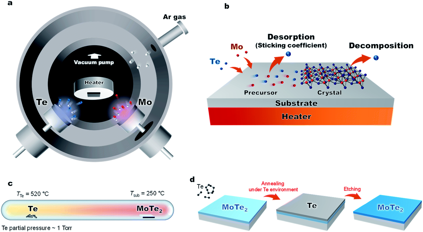 | ||
| Fig. 1 (a) Schematic diagram of the low-energy sputtering deposition. (b) MoTe2 growth is limited by a tellurium deficiency due to (1) Te desorption from a precursor state and (2) decomposition of fully-reacted MoTex. (c) Diagram of the post annealing process of the MoTe2 film under Te pressure. (d) Post thermal process and Te etching process. | ||
Fig. 1a and 3a show the schematic diagram of the deposition chamber and the most-often used temperature timetable, respectively. The ultra-high vacuum (UHV) chamber is evacuated to a low 10−7 torr range prior to deposition, followed by sputtering. In our studies, elevated Ar pressures of 150 mTorr were used during the sputtering process to decrease the deposition rate and reduce the kinetic energy of the impinging species on the growth surface. The latter is important to minimize surface and subsurface damage to the growing film, while potentially enhancing surface diffusion. The deposition rate of each element is dependent on sputter power. With increased sputter power of the Te source, we observed effects of charge build-up on the Te target, which caused rather unpredictable deposition rates. To avoid this charge buildup, the Te sputter power was fixed to 5 W while using a DC sputtering source. The effects of the Mo sputter power on the crystal quality and Te/Mo ratio were studied and we optimized the conditions (Fig. S2†).
Sticking coefficient and decomposition rate
The sticking coefficient is determined by the adsorption energy of precursor atoms (Mo and Te atoms) on the growth surface. The decomposition rate is determined by the energy of the atoms that are part of the fully reacted MoTe2 phase, and is indistinguishable from the evaporation rate of a bulk solid. These two factors ultimately dictate growth characteristics and are two critical parameters for the establishment of a controllable growth process.26 To determine these growth parameters and access the Mo and Te sticking coefficients and decomposition rates, the amount of Mo and Te evaporated and deposited was measured during co-sputtering onto graphite/sapphire and bare c-cut sapphire substrates at substrate temperatures ranging from room temperature to 450 °C (Fig. 2a).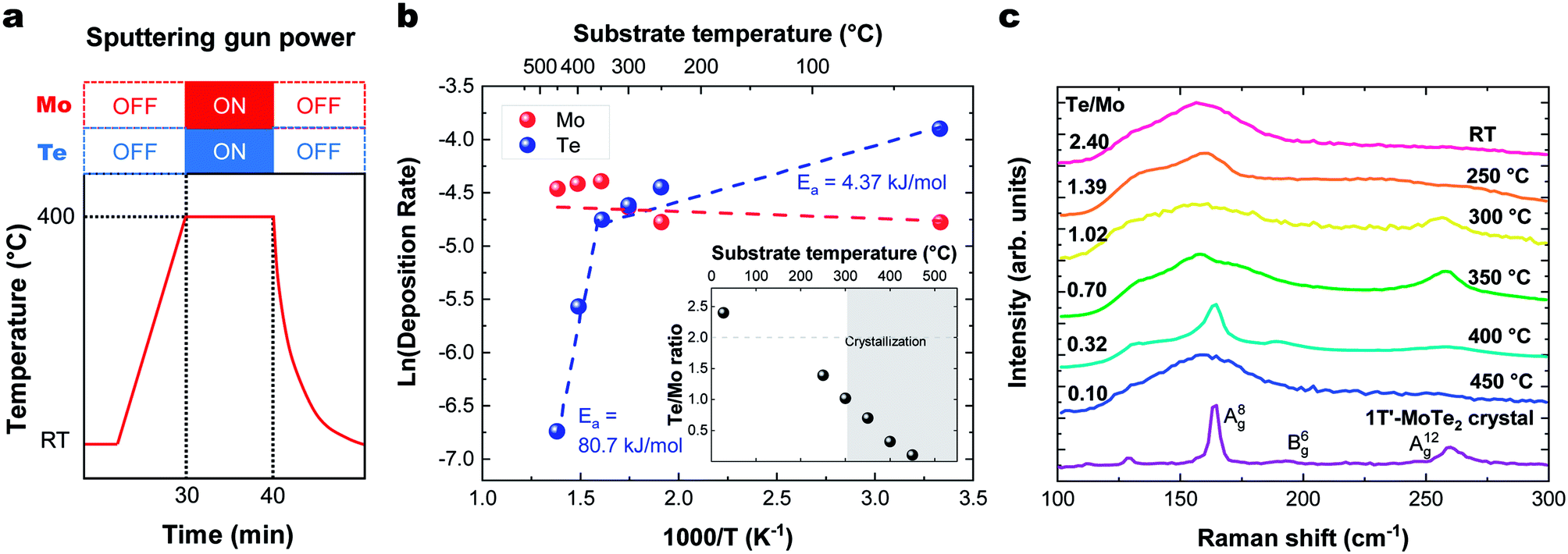 | ||
| Fig. 2 (a) Temperature profile for sticking coefficient measurement. Substrate temperature dependence of (b). the Arrhenius plot of deposition rate vs. temperature on (inset) the Te/Mo ratio. Deposition rate is the number of atoms divided by the deposition time (×1015 atoms per cm2 per s). (c) Raman spectra of MoTe2 films deposited at different temperatures. | ||
The typical thickness of the deposited Mo/Te film was approximately a few nanometers, as determined by Rutherford backscattering spectroscopy (RBS). The number of Mo and Te atoms deposited on sapphire substrates per unit area is measured by RBS, then divided by the growth time to determine the deposition rates. By taking the slope of an Arrhenius plot of the deposition rate, we extracted the activation energy for decomposition,  as shown in Fig. 2b. Closer inspection of this figure reveals two main properties: (1) first, it can be seen that the Mo deposition rate (red circles in Fig. 2b) is nearly independent of the substrate temperature, while the Te deposition rate significantly decreases above 300 °C. Tellurium metal has a high vapor pressure at low temperatures (∼10−2 torr at 400 °C), while Mo's is very small (extrapolated to be ∼10−40 torr at 400 °C). The normalized Te sticking coefficient, referenced to the room temperature deposition rate, decreases with temperature to a low coefficient of 0.58 at 450 °C. This results in highly Te deficient MoTe2 films. (2) The Arrhenius plot for Te shows that there are two distinct slopes with two different activation energies (Fig. 2b blue circles). The lower activation energy (Ea = 4.3 kJ mol−1) is well-defined between 20 °C and 350 °C and is related to the desorption of the precursor forms of tellurium from the growth surface, often referred to as the sticking coefficient. We attribute the higher activation energy (Ea = 80.7 kJ mol−1) to the evaporation of Te as a result of the thermal decomposition of MoTe2−x.
Raman data collected on these films deposited in a range of temperatures (Fig. 2c) show that crystallization occurs at 300 °C and above, as evidenced by the emergent of out-of-plane A(8)g (163 cm−1) and A(12)g (259 cm−1) phonon modes. In-plane B(6)g (190 cm−1) modes of 1T′-MoTe2 were observed at 400 °C. The Raman spectra of the films deposited on HOPG and sapphire showed similar substrate temperature dependence and Raman spectra. These Raman peaks match with the literature values.27 This absence of Raman peaks in films deposited below 300 °C and above 450 °C indicates that the associated films do not contain significant levels of crystalline MoTe2. For low temperature growth, there is not enough thermal energy available to overcome the kinetic barriers of thin film growth (e.g. surface diffusion and reaction). And for high temperature growth, Te-poor films are formed as a result of the high MoTex decomposition rate.
MoTe2 film deposition at room temperature followed by in situ annealing
To produce a film with better stoichiometry, we co-sputtered Mo and Te at room temperature, where the sticking coefficient is high, followed by an in situ annealing. The temperature profile of this process and corresponding deposition rate and Te/Mo ratio on the sapphire substrate are shown in Fig. 3a and b, respectively. We note that there were no observable differences in the deposition rate or Te/Mo ratio when MoTe2 was deposited onto sapphire and HOPG substrates. Similar to the previous section, our findings reveal that there are two activation energies for Te. One low energy desorption process and another higher energy decomposition process that dominates above 300 °C. The experiments support the following observations: (1) Mo and Te atoms deposited at room temperature have a sticking coefficient near 1 and (2) annealing of the composite in the range of 300–350 °C provides sufficient energy to facilitate a reaction, without experiencing a high Te desorption rate. This allows us to produce MoTe2−x thin films with a high Te/Mo ratio (x < 0.3).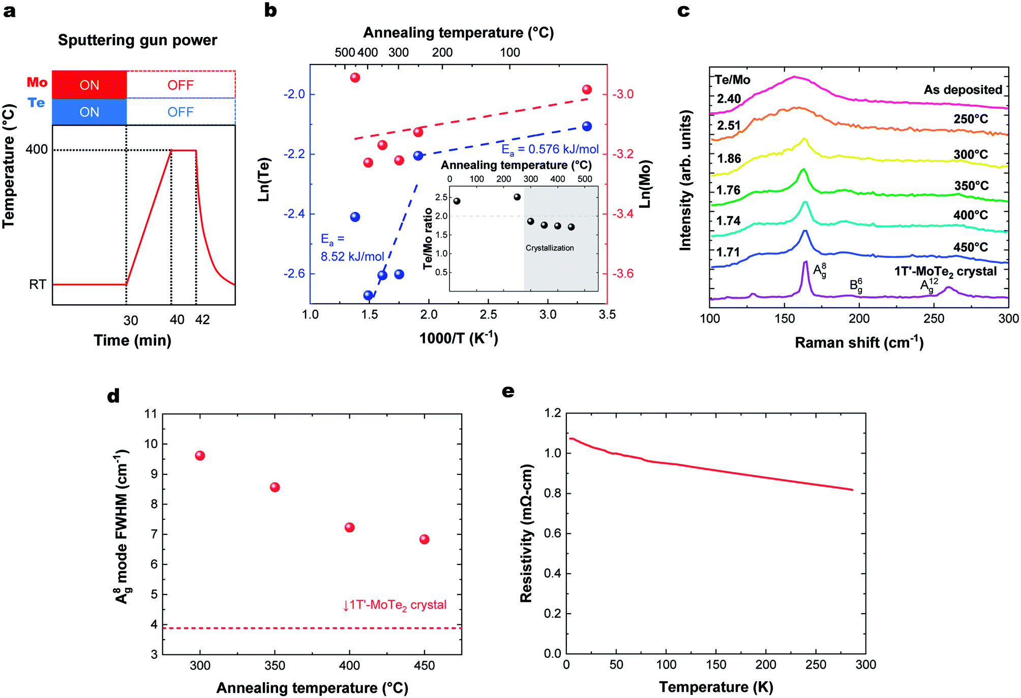 | ||
| Fig. 3 (a) Temperature profile for MoTe2 thin film growth followed by in situ annealing. (b) Annealing temperature dependence of Te and Mo deposition rates, with (inset) the number of atoms and Te/Mo ratio, where Te and Mo are the number of Te, Mo atoms on the substrate divided by the deposition time (×1015 atoms per cm2 per s). (c) Raman spectra. (d) Annealing temperature dependence of A(8)g Raman peak width. (e) Temperature dependence of resistivity of deposited MoTe2. | ||
The degree of crystallization of 1T′ MoTe2 can best be monitored by observing the temperature-dependence of the Raman spectrum above 300 °C (Fig. 3c). Raman spectra of the films for HOPG and sapphire showed a similar substrate temperature dependence and Raman spectra (Fig. S2†). The minimum crystallization temperature of ∼300 °C is similar to that found when Mo and Te are sputtered onto heated substrates, as described above. The Raman peak width represents a gauge of the crystallinity of the films, as defects and grain boundaries create local strain and broaden Raman peaks. The crystallinity of the films as a function of annealing temperature was analyzed using the figure-of-merit of FWHM of the A(8)g mode,15,17,28,29 as shown in Fig. 3d. The crystallinity of MoTe2 films improves with increasing annealing, and we do not find any deterioration of MoTe2 crystal quality up to 450 °C. Thus, room temperature co-sputtering followed by an in situ annealing process can be used to grow 1T′-MoTe2 films. The thickness of the MoTe2 films can be precisely controlled from an order of a nanometer to tens of nanometers by adjusting the sputtering time.
Fig. 3e shows the temperature dependence of the resistivity of a deposited MoTe2 film. Raman spectra in the previous section indicated that the deposited films form in the 1T′ metallic phase. However, the ρ–T plot shows an increase in resistivity at lower temperatures, which is characteristic of carrier concentrations lower than the metal-insulator transition.30 This can be attributed to doping of the material by the VTe, consistent with the Te-poor stoichiometry measured with RBS.
The origin of 1T′-phase stabilization: charge driven 2H → 1T′ phase transition
Here we discuss why the high-temperature 1T′ phase forms during the growth reported in this study. As shown by the phase diagram in Fig. 4a, the 2H phase is formed at temperatures lower than that of the 1T′-phase. When the substrate is cooled down to room temperature, the materials would thus be expected to form the 2H-phase alone. However, we observe the presence of only the 1T′-MoTe2 phase, presumably as a result of the stabilization of this phase by the presence of the VTe donors.16,31 This has previously been documented using ionic gating experiments on exfoliated 2H-MoTe2 flakes when the sheet electron density is greater than 2.2 × 1014 cm−2.14 Hall measurements on our MoTe2 films show that our sheets contain n-type carriers with a concentration of 4.6 × 1014 cm−2. Kelvin probe force microscopy (KPFM) data collected from sputtered MoTe2 and exfoliated 1T′-MoTe2 (Fig. 4d–f) show that the work function of sputtered MoTe2 is lower than that of exfoliated 1T′ by 130 meV, indicating that the deposited MoTe2 film is decisively n-doped. For a film with a Te/Mo ratio of 1.76, the estimated density of the double-donor VTe per layer is 2.7 × 1014 cm−2, resulting in a free-electron density of 5.4 × 1014 cm−2. This is also consistent with recent reports on exfoliated MoTe2 sheets that find that a ∼3% VTe concentration is sufficient to stabilize the 1T′-phase over the 2H-MoTe2 phase.1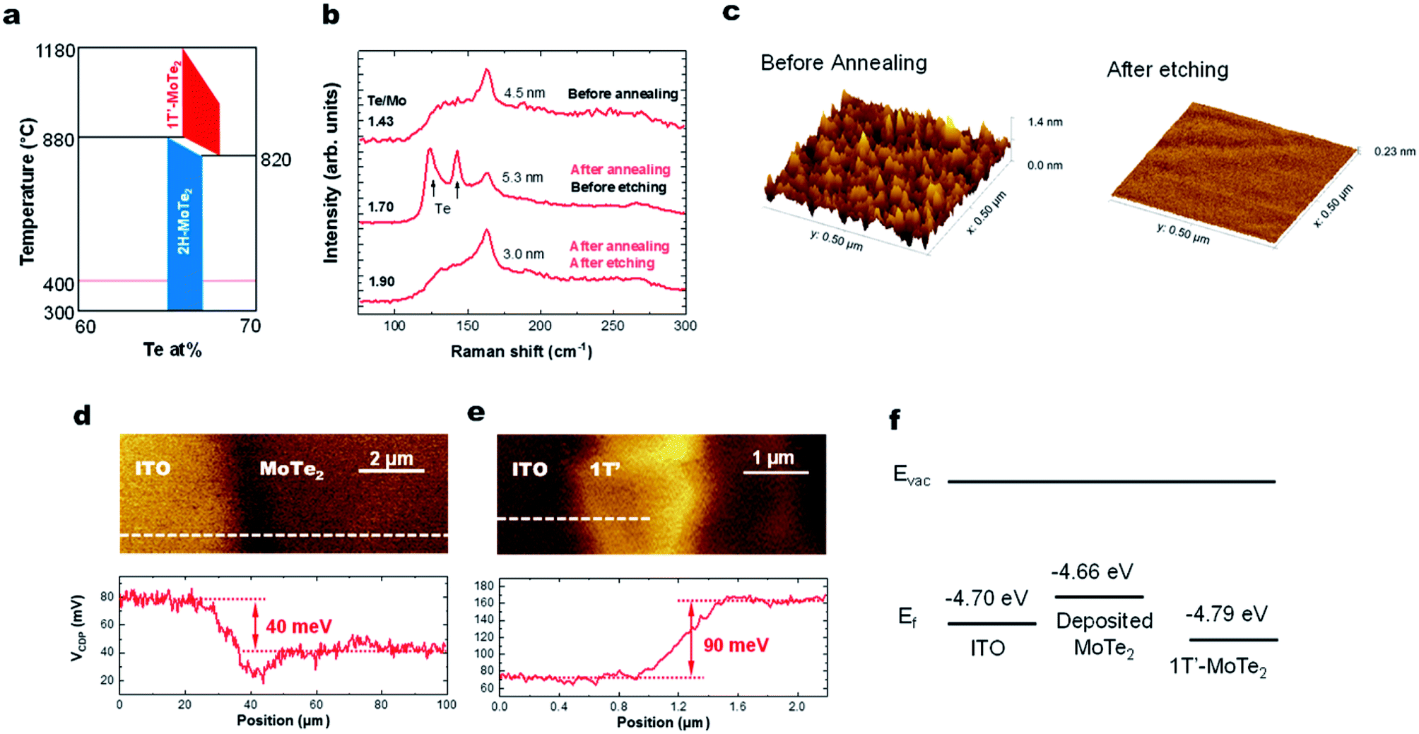 | ||
| Fig. 4 (a) Phase diagram of MoTe2. (b) Raman spectra before/after annealing and the etching process. (c) AFM image of the MoTe2 films before annealing and after the etching process. KPFM image of (d) deposited MoTe2 and (e) exfoliated 1T′-MoTe2 crystals. (f) Fermi energies of ITO, deposited MoTe2 film and exfoliated MoTe2 crystals. | ||
Improving the stoichiometry by high pressure Te annealing
Lastly, we show that the stoichiometry can be further improved using ex situ thermal processing. A MoTe2 film was deposited at room temperature, in situ annealed at 400 °C and then sealed in a glass ampoule with elemental Te and heated at high temperatures (Fig. 1c). A ∼1 torr Te partial pressure in the ampoule was produced by keeping the Te side at 520 °C. The side with the MoTe2 film was kept at 250 °C. A thin Te overlayer was formed on the MoTe2 film, which was subsequently removed using H2SO4 (Fig. 4b). During the treatment, excess Mo was removed by H2SO4 and the Te/Mo ratio of the film increased even though a Te overlayer was removed. After the treatment, the film surface was found to be smoother (Fig. 4c), the MoTe2 stoichiometry increased to MoTe1.90 and the structure remained in the 1T′ phase, but there was no noticeable change in the Raman FWHM values. Despite the improvement, this value still remains above the 3% vacancy threshold which was previously suggested for stabilizing the 1T′ phase.Conclusion
The overall results have established a low temperature soft sputtering technique that can synthesize MoTe2 films. The process can produce 2D anisotropic MoTe2 1T′ phase films using room-temperature co-sputtering of Te and Mo under relatively high pressure, followed by in situ annealing. This industrially compatible sputtering method offers large area growth capability, thickness control, freedom in substrate selection, and the ability to adjust the stoichiometry. Activation energies for film decomposition were determined by measuring the incorporation rate of Mo and Te into MoTe2 films on heated substrates. The crystallization of these MoTe2 films required temperatures greater than 300 °C and the deposited MoTe2 has always crystallized in the 1T′ anisotropic phase as a result of stabilization by using a high concentration of VTe double-donors. Ex situ thermal annealing in a high-pressure Te environment increased the stoichiometry of the 1T′ phase from MoTe1.86 to MoTe1.90.Conflicts of interest
There are no conflicts of interest declared.Acknowledgements
S. T. acknowledges partial funding from the NSF DMR-1552220. We acknowledge the use of the facilities in the Eyring Materials Center at Arizona State University supported in part by the NNCI-ECCS-1542160.References
- X. Xu, S. Chen, S. Liu, X. Cheng, W. Xu, P. Li, Y. Wan, S. Yang, W. Gong, K. Yuan, P. Gao, Y. Ye and L. Dai, J. Am. Chem. Soc., 2019, 141, 2128–2134 CrossRef CAS PubMed.
- J. Young and T. L. Reinecke, Phys. Chem. Chem. Phys., 2017, 19, 31874–31882 RSC.
- T. Mueller and E. Malic, npj 2D Mater. Appl., 2018, 2, 29 CrossRef.
- K. F. Mak, K. He, C. Lee, G. H. Lee, J. Hone, T. F. Heinz and J. Shan, Nat. Mater., 2013, 12, 207–211 CrossRef CAS PubMed.
- K. F. Mak, C. Lee, J. Hone, J. Shan and T. F. Heinz, Phys. Rev. Lett., 2010, 105, 136805 CrossRef PubMed.
- B. Yan and C. Felser, Annu. Rev. Condens. Matter Phys., 2017, 8, 337–354 CrossRef.
- M. Hossain, Z. Zhao, W. Wen, X. Wang, J. Wu and L. Xie, Crystals, 2017, 7, 298 CrossRef.
- A. Zong, X. Shen, A. Kogar, L. Ye, C. Marks, D. Chowdhury, T. Rohwer, B. Freelon, S. Weathersby, R. Li, J. Yang, J. Checkelsky, X. Wang and N. Gedik, Sci. Adv., 2018, 4, eaau5501 CrossRef CAS PubMed.
- J. A. Wilson, Philos. Trans. R. Soc., A, 1985, 314, 159 CrossRef.
- M. Waldherr, N. Lundt, M. Klaas, S. Betzold, M. Wurdack, V. Baumann, E. Estrecho, A. Nalitov, E. Cherotchenko, H. Cai, E. A. Ostrovskaya, A. V. Kavokin, S. Tongay, S. Klembt, S. Höfling and C. Schneider, Nat. Commun., 2018, 9, 3286 CrossRef PubMed.
- J. Kopaczek, M. P. Polak, P. Scharoch, K. Wu, B. Chen, S. Tongay and R. Kudrawiec, J. Appl. Phys., 2016, 119, 235705 CrossRef.
- S. Tongay, J. Zhou, C. Ataca, K. Lo, T. S. Matthews, J. B. Li, J. C. Grossman and J. Q. Wu, Nano Lett., 2012, 12, 5576–5580 CrossRef CAS PubMed.
- A. Chernikov, T. C. Berkelbach, H. M. Hill, A. Rigosi, Y. Li, O. B. Aslan, D. R. Reichman, M. S. Hybertsen and T. F. Heinz, Phys. Rev. Lett., 2014, 113, 076802 CrossRef PubMed.
- P. Li, Y. Wen, X. He, Q. Zhang, C. Xia, Z.-M. Yu, S. A. Yang, Z. Zhu, H. N. Alshareef and X.-X. Zhang, Nat. Commun., 2017, 8, 2150 CrossRef PubMed.
- C. Ruppert, O. B. Aslan and T. F. Heinz, Nano Lett., 2014, 14, 6231–6236 CrossRef CAS PubMed.
- Y. Wang, J. Xiao, H. Zhu, Y. Li, Y. Alsaid, K. Y. Fong, Y. Zhou, S. Wang, W. Shi, Y. Wang, A. Zettl, E. J. Reed and X. Zhang, Nature, 2017, 550, 487 CrossRef CAS PubMed.
- B. Chen, H. Sahin, A. Suslu, L. Ding, M. I. Bertoni, F. M. Peeters and S. Tongay, ACS Nano, 2015, 9, 5326–5332 CrossRef CAS PubMed.
- S. Tang, C. Zhang, D. Wong, Z. Pedramrazi, H.-Z. Tsai, C. Jia, B. Moritz, M. Claassen, H. Ryu, S. Kahn, J. Jiang, H. Yan, M. Hashimoto, D. Lu, R. G. Moore, C.-C. Hwang, C. Hwang, Z. Hussain, Y. Chen, M. M. Ugeda, Z. Liu, X. Xie, T. P. Devereaux, M. F. Crommie, S.-K. Mo and Z.-X. Shen, Nat. Phys., 2017, 13, 683 Search PubMed.
- N. Briggs, S. Subramanian, Z. Lin, X. Li, X. Zhang, K. Zhang, K. Xiao, D. Geohegan, R. Wallace, L.-Q. Chen, M. Terrones, A. Ebrahimi, S. Das, J. Redwing, C. Hinkle, K. Momeni, A. van Duin, V. Crespi, S. Kar and J. A. Robinson, 2D Materials, 2019, 6, 022001 Search PubMed.
- Y.-H. Lee, X.-Q. Zhang, W. Zhang, M.-T. Chang, C.-T. Lin, K.-D. Chang, Y.-C. Yu, J. T.-W. Wang, C.-S. Chang, L.-J. Li and T.-W. Lin, Adv. Mater., 2012, 24, 2320–2325 CrossRef CAS PubMed.
- F. Zhang, K. Momeni, M. A. AlSaud, A. Azizi, M. F. Hainey, J. M. Redwing, L.-Q. Chen and N. Alem, 2D Materials, 2017, 4, 025029 CrossRef.
- D. Dumcenco, D. Ovchinnikov, K. Marinov, P. Lazić, M. Gibertini, N. Marzari, O. L. Sanchez, Y.-C. Kung, D. Krasnozhon, M.-W. Chen, S. Bertolazzi, P. Gillet, A. Fontcuberta i Morral, A. Radenovic and A. Kis, ACS Nano, 2015, 9, 4611–4620 CrossRef CAS PubMed.
- L. Zhou, A. Zubair, Z. Wang, X. Zhang, F. Ouyang, K. Xu, W. Fang, K. Ueno, J. Li, T. Palacios, J. Kong and M. S. Dresselhaus, Adv. Mater., 2016, 28, 9526–9531 CrossRef CAS PubMed.
- S. Hussain, S. A. Patil, D. Vikraman, N. Mengal, H. Liu, W. Song, K.-S. An, S. H. Jeong, H.-S. Kim and J. Jung, Sci. Rep., 2018, 8, 29 CrossRef PubMed.
- J. Y. Tsao, Materials Fundamentals of Molecular Beam Epitaxy, Academic Press, New York, 1993 Search PubMed.
- B. Scherwitzl, R. Resel and A. Winkler, J. Chem. Phys., 2014, 140, 184705 CrossRef PubMed.
- X. Ma, P. Guo, C. Yi, Q. Yu, A. Zhang, J. Ji, Y. Tian, F. Jin, Y. Wang, K. Liu, T. Xia, Y. Shi and Q. Zhang, Phys. Rev. B, 2016, 94, 214105 CrossRef.
- P. Miao, J.-K. Qin, Y. Shen, H. Su, J. Dai, B. Song, Y. Du, M. Sun, W. Zhang, H.-L. Wang, C.-Y. Xu and P. Xu, Small, 2018, 14, 1704079 CrossRef PubMed.
- R. Beams, L. G. Cançado, S. Krylyuk, I. Kalish, B. Kalanyan, A. K. Singh, K. Choudhary, A. Bruma, P. M. Vora, F. Tavazza, A. V. Davydov and S. J. Stranick, ACS Nano, 2016, 10, 9626–9636 CrossRef CAS PubMed.
- L. Wang, I. Gutierrez-Lezama, C. Barreteau, N. Ubrig, E. Giannini and A. F. Morpurgo, Nat. Commun., 2015, 6, 8892 CrossRef PubMed.
- Y. Li, K.-A. N. Duerloo, K. Wauson and E. J. Reed, Nat. Commun., 2016, 7, 10671 CrossRef CAS PubMed.
Footnotes |
| † Electronic supplementary information (ESI) available. See DOI: 10.1039/d0na00066c |
| ‡ These authors contributed to this work equally. |
| This journal is © The Royal Society of Chemistry 2020 |