
 Open Access Article
 This Open Access Article is licensed under a Creative Commons Attribution-Non Commercial 3.0 Unported Licence
A broadband ultraviolet light source using GaN quantum dots formed on hexagonal truncated pyramid structures†
Jong-Hoi
Cho‡
a,
Seung-Hyuk
Lim‡§
a,
Min-Ho
Jang
a,
Chulwon
Lee
a,
Hwan-Seop
Yeo
a,
Young Chul
Sim
a,
Je-Hyung
Kim
a,
Samuel
Matta
b,
Blandine
Alloing
b,
Mathieu
Leroux
b,
Seoung-Hwan
Park
c,
Julien
Brault
b and
Yong-Hoon
Cho
 *a
*a
aDepartment of Physics, KI for the NanoCentury, Korea Advanced Institute of Science and Technology (KAIST), Daejeon 34141, Republic of Korea. E-mail: yhc@kaist.ac.kr
bUniversité Côte d'Azur, CNRS, CRHEA, 06560 Valbonne, France
cDepartment of Electronics Engineering, Catholic University of Daegu, Kyeongsan 38430, Republic of Korea
First published on 11th February 2020
Abstract
Group III-nitride semiconductor-based ultraviolet (UV) light emitting diodes have been suggested as a substitute for conventional arc-lamps such as mercury, xenon and deuterium arc-lamps, since they are compact, efficient and have a long lifetime. However, in previously reported studies, group III-nitride UV light emitting diodes did not show a broad UV spectrum range as conventional arc-lamps, which restricts their application in fields such as medical therapy and UV spectrophotometry. Here, we propose GaN quantum dots (QDs) grown on different facets of hexagonal truncated pyramid structures formed on a conventional (0001) sapphire substrate. A hexagonal truncated GaN pyramid structure includes {10![[1 with combining macron]](https://www.rsc.org/images/entities/char_0031_0304.gif) 1} semipolar facets as well as a (0001) polar facet, which have intrinsically different piezoelectric fields and growth rates of GaN QDs. Consequently, we successfully demonstrated a plateau-like broadband UV spectrum ranging from ∼400 nm (UV-A) to ∼270 nm (UV-C) from the GaN QDs. In addition, at the top-edge of the truncated pyramid structure, a strain was locally suppressed compared to the center of the truncated pyramid structure. As a result, various emission wavelengths in the UV range were achieved from the GaN QDs grown on the sidewall, top-edge and top-center of hexagonal truncated pyramid structures, which ultimately provide a broadband UV spectrum with high efficiency.
1} semipolar facets as well as a (0001) polar facet, which have intrinsically different piezoelectric fields and growth rates of GaN QDs. Consequently, we successfully demonstrated a plateau-like broadband UV spectrum ranging from ∼400 nm (UV-A) to ∼270 nm (UV-C) from the GaN QDs. In addition, at the top-edge of the truncated pyramid structure, a strain was locally suppressed compared to the center of the truncated pyramid structure. As a result, various emission wavelengths in the UV range were achieved from the GaN QDs grown on the sidewall, top-edge and top-center of hexagonal truncated pyramid structures, which ultimately provide a broadband UV spectrum with high efficiency.
Introduction
Group III-nitride semiconductor-based ultraviolet (UV) light emitting diodes (LEDs) have received significant attention in recent years as a substitute for conventional arc-lamps such as mercury, xenon and deuterium arc-lamps.1–4 UV LEDs can be extensively used for numerous UV applications such as polymer curing, sterilization1 and photolithography.2,3 In general, group III-nitride semiconductors have large defect density due to lattice mismatch and thermal expansion difference with respect to foreign substrates such as sapphire, SiC, Si, etc. In this respect, some research studies have focused on quantum dot (QD) based LEDs since the QDs enable strong carrier localization,5,6 which prohibits carriers from being captured by defects. In addition, their emission wavelength can be manipulated via the quantum effect in QDs.7–9 Indeed, the emission wavelength of GaN QDs can be shorter than the GaN band-edge emission due to the quantum-confinement effect,9 but can also be longer due to the presence of an internal electric field and the consequent quantum confined Stark effect.9,10 As a result, the emission wavelength of GaN QDs grown on a (0001) polar sapphire substrate has remained in the UV-A range.11 For deeper UV emission, GaN QDs grown on unconventional substrates with nonpolar or semipolar planes can be adopted, which have a negligible internal electric field. Although various methods for manipulating the emission wavelength have been suggested, previous studies have focused only on achieving a narrow UV emission spectrum. As a result, the emission spectrum range of UV LEDs is not as broad as that of conventional arc-lamps, and thus the need for achieving a solid-state based broadband UV light source still remains. Because of the spectral limitations of conventional UV LEDs, some applications such as UV spectrophotometry12,13 and photodynamic therapy in dermatology14,15 still require arc-lamps even though the arc-lamp system is impractical and inefficient due to their bulky system, heat generation and poor lifetime.Here, we propose a combination of GaN/AlGaN QDs grown on GaN-based hexagonal truncated pyramid structures for a solid-state broadband UV light source. In this structure, GaN QDs were used as active layers embedded in AlxGa1−xN (x ∼ 0.5, nominal composition) matrix layers.16,17 Although a c-plane sapphire substrate was used, the GaN-based hexagonal truncated pyramid structures include (0001) polar and {101} semipolar facets, which have intrinsically different internal electric fields as well as growth rates depending on the facet.18 Therefore, the GaN QDs grown on different facets show various UV emission wavelengths and structural properties. In particular, the GaN QDs grown on the top-edge of the hexagonal truncated pyramid structures have locally suppressed strain, and have distinct properties from those at the top-center of these structures in spite of the same (0001) polar facet. Based on these unique properties, we successfully demonstrate a plateau-like broadband UV spectrum covering the wavelength range from ∼400 nm (UV-A) to ∼270 nm (UV-C) and expect to replace many arc-lamp-based applications.
Results and discussion
Fig. 1a–c show the fabrication process of the GaN QDs on GaN-based hexagonal truncated pyramid structures for the broadband UV light source device. To fabricate such a unique structure, we combined both a selective area growth technique18 by metal–organic chemical vapor deposition (MOCVD) and a 2D–3D growth mode transition, i.e. equivalent to the so-called Stranski–Krastanov (SK) growth technique, using molecular beam epitaxy (MBE). After a GaN template was first grown on a c-sapphire substrate by MOCVD, a SiNx layer was deposited and hole patterns with 20 μm diameter were fabricated by lithography and dry etching. The hexagonal truncated pyramid GaN structures were formed by a second MOCVD process. After a nominal 175 nm AlN buffer layer was grown by MBE on the GaN truncated pyramid structures to avoid cracks, a nominal 810 nm-thick AlxGa1−xN (x ∼ 0.5, nominal composition) layer was grown. Two layers containing GaN QDs, using a deposited GaN amount of six monolayers (i.e. with one monolayer corresponding approximately to 0.25 nm), were formed on these truncated pyramid structures by triggering a 2D–3D “SK type” growth mode transition19 separated by a 30 nm-thick AlxGa1−xN quantum barrier. In between these GaN QDs, a thin wetting layer of a few monolayers composed of GaN was formed, which is a typical signature of the 2D–3D morphological transition of the deposited GaN layer.16 By not capping the last QD layer, the geometric morphology of the GaN QDs can be investigated.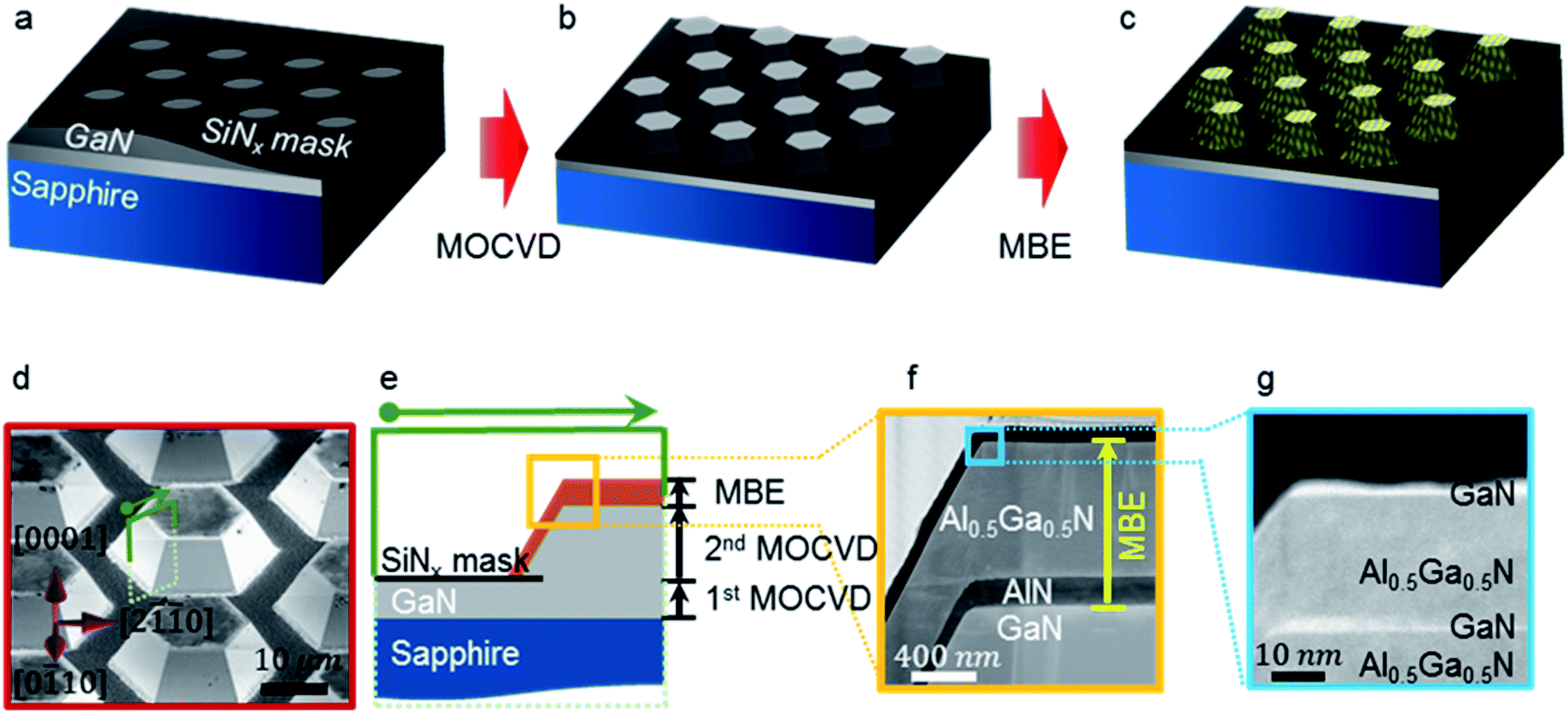 | ||
| Fig. 1 Schematics of the fabrication process of GaN QDs on truncated pyramids. (a) Hole patterned SiNx layer deposited on the 1st MOCVD-grown GaN template. (b) 2nd MOCVD growth: selective area growth for GaN truncated pyramids. (c) MBE growth: AlN/AlxGa1−xN/GaN QDs. (d) Bird's eye view SEM image of GaN QDs on truncated pyramid structures. (e) Cross-sectional schematic of GaN QDs on a truncated pyramid structure indicated with a green box and arrow in (d). (f) Cross-sectional HAADF STEM image of an MBE-grown region indicated with a yellow box in (e). (g) Magnified HAADF STEM image of the boundary between the (0001) polar and {101} semipolar facets indicated with a blue box in (f). | ||
An overall tilted scanning electron microscopy (SEM) image of the sample after the MOCVD and MBE growth is shown in Fig. 1d. The truncated pyramid structure mainly consists of two types of facets, (0001) polar and {101} semipolar facets. Fig. 1e shows a cross-sectional schematic (location and direction indicated with the green box and the arrow in Fig. 1d) along the 〈1![[2 with combining macron]](https://www.rsc.org/images/entities/char_0032_0304.gif) 10〉 axis. A high angle annular dark field scanning transmission electron microscopy (HAADF STEM) image was taken at the boundary between the (0001) polar and {101} semipolar facets (the yellow square in Fig. 1e) as shown in Fig. 1f. With clear contrast, we confirmed that the AlN and AlxGa1−xN layers grown by MBE were successfully fabricated on the MOCVD-grown GaN structure. Two sets of QD layers were also observed in the magnified HAADF STEM image (Fig. 1g).
10〉 axis. A high angle annular dark field scanning transmission electron microscopy (HAADF STEM) image was taken at the boundary between the (0001) polar and {101} semipolar facets (the yellow square in Fig. 1e) as shown in Fig. 1f. With clear contrast, we confirmed that the AlN and AlxGa1−xN layers grown by MBE were successfully fabricated on the MOCVD-grown GaN structure. Two sets of QD layers were also observed in the magnified HAADF STEM image (Fig. 1g).
Fig. 2a shows the top-view SEM image of an entire single truncated pyramid structure. As shown in Fig. 2b, the GaN QDs grown on the (0001) polar facet (P-QDs) were densely formed on the surface. Interestingly, we found one or two rows of QDs within 200 nm width along the boundary line between the (0001) polar and {101} semipolar facets, which are spatially distinguished from the P-QDs. In other words, these QDs were formed along the boundary line, while the other P-QDs were randomly formed on the surface (see ESI Fig. S1†). Given this distinction, we named those QDs grown on the boundary region B-QDs. In the case of the QDs grown on the {101} semipolar facets (S-QDs), a few S-QDs have comparable size to that of the P-QDs. But, most of the S-QDs were too small to be clearly observed by SEM.
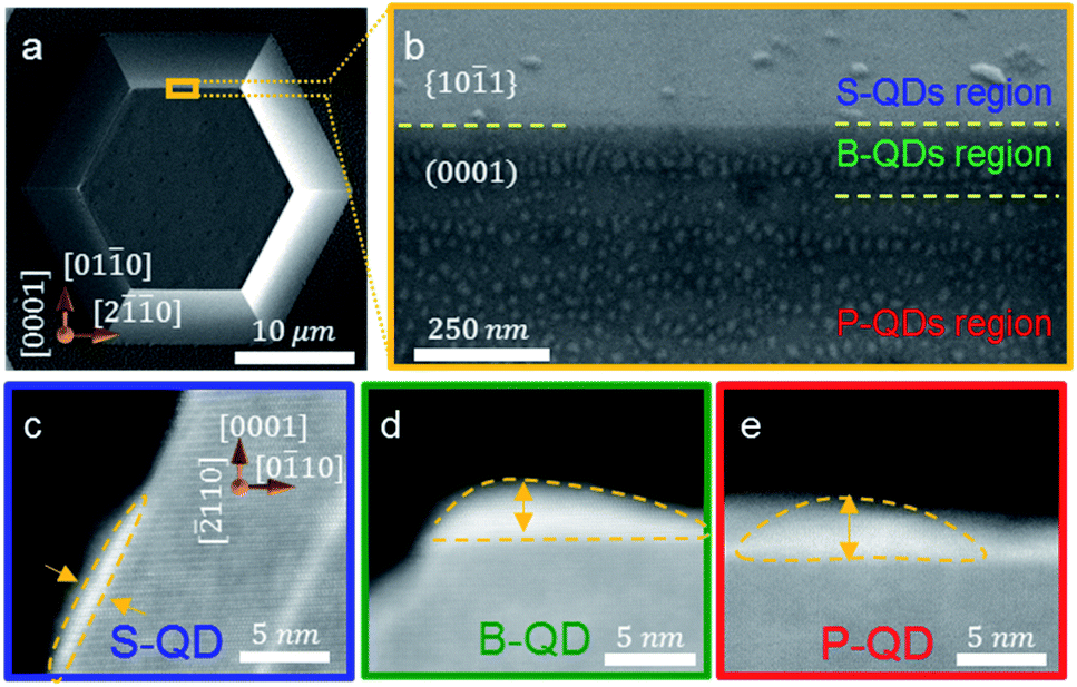 | ||
| Fig. 2 (a) Top-view SEM image of a single truncated pyramid. (b) High-resolution SEM image of the boundary between (0001) polar and {101} semipolar facets. (c–e) HAADF STEM images of S-, B-, and P-QDs on the surface of the truncated pyramid, respectively. | ||
To clarify the morphological characteristics of the S-, B-, and P-QDs, HAADF STEM was conducted. Fig. 2c–e present the HAADF STEM images of single S-, B-, and P-QDs, respectively. The average heights of the S-, B- and P-QDs are 1.09 ± 0.25 nm, 2.57 ± 0.20 nm, and 2.91 ± 0.47 nm, respectively. Since the HAADF STEM sample was prepared using a focused ion beam along [010], dozens of S-QDs and P-QDs were checked to measure their heights but only two B-QDs were measured because of the tiny boundary region. The height of the S-QDs was approximately one-third smaller than that of B- and P-QDs because of the angled source flux during MBE. This height ratio corresponds to the thickness ratio of the AlN and AlxGa1−xN layers between the (0001) polar and {101} semipolar facets, which was about one-third (Fig. 1f).
We measured photoluminescence (PL) and PL excitation (PLE) spectra at 10 K as shown in Fig. 3. A plateau-like broadband UV emission ranging from UV-A to UV-C was observed as shown in Fig. 3a. When measuring the monochromatic cathodoluminescence (CL) images at 10 K, the emission regions of each wavelength could be spatially distinguished, as shown in Fig. 3b–f. The emission wavelengths of S-, B- and P-QDs revealed a blue-shift from the bulk GaN peak because of the quantum confinement effect.9,10 The emission wavelength of S-QDs was shorter than those of the B- and P-QDs due to the smaller height of S-QDs and the negligible built-in electric field of {101} semipolar facets.8
 | ||
| Fig. 3 (a) PL and PLE spectra at 10 K. The black line shows the broadband UV emission spectrum. Blue and green lines indicate the PLE intensity of S- and B-QDs, respectively. DAP stands for donor-to-acceptor pair. (b–f) Low-temperature (10 K) monochromatic CL images of a single truncated pyramid measured at 280 nm, 293 nm, 313 nm, 330 nm, and 340 nm, respectively (scale bars: 10 μm). | ||
Interestingly, we found that the emission wavelength of B-QDs was clearly distinguished from those of P-QDs or S-QDs, as shown in Fig. 3e. The emission wavelength of B-QDs is shorter than that of P-QDs even though they were grown on the same (0001) polar facet. Furthermore, the CL emission from the AlGaN layer is also distinguished at the boundary region, energetically as well as spatially, from the other regions (i.e. top and side facets of the pyramid) as shown in Fig. 3c. This indicates that the Al composition of the AlGaN layer surrounding B-QDs is lower than that of the layer surrounding P-QDs and S-QDs. Due to the lower-Al-content AlGaN layer surrounding B-QDs, the lattice difference between the B-QDs and AlGaN layer decreases, which leads to the reduction of the piezoelectric field of B-QDs. Consequently, the emission wavelength of B-QDs is less affected by the quantum confined Stark effect and is shorter than that of P-QDs despite occupying the same (0001) polar facet. In addition, the average height of P-QDs is higher than that of B-QDs, which also modifies the QD emission and leads to longer wavelengths in the case of P-QDs.20
To clarify the relationship between the QDs and AlGaN layers, PLE spectra were measured. In Fig. 3a, PLE spectra detected at 311 nm (blue line) and 328 nm (green line) are shown, which correspond to the emission peaks of S- and B-QDs, respectively. The PLE intensity of S-QDs dramatically decreased at ∼275 nm (the blue arrow), which is the absorption band edge of the AlGaN layer surrounding S-QDs. On the other hand, the PLE intensity of B-QDs decreased at ∼287 nm (the green arrow) corresponding to the absorption band edge of the AlGaN layer surrounding B-QDs. These PLE results are well consistent with the CL results. We emphasize that the distinct optical properties of B-QDs in relation to S- and P-QDs originated from combined differences in the surrounding AlGaN layers and the QD average heights.
For a more detailed inspection, Fig. 4a shows the HRTEM image taken near the edge of the truncated pyramid structure. According to a previous study,21 the QDs located on the boundary region of a truncated pyramid structure can release strain during the QD formation process. In this respect, the selective area diffraction (SAD) patterns of the AlxGa1−xN layers below B- and P-QDs were measured to compare the lattice difference, as shown in Fig. 4b and c, respectively. The AlxGa1−xN layer lattice distance between the two (010) planes below B-QDs was +0.65% larger than that below P-QDs. On the other hand, along (0002) planes, the AlxGa1−xN layer lattice distance below B-QDs was −0.64% smaller than that below P-QDs. This indicates that the AlxGa1−xN layer below B-QDs was laterally stretched, which consequently reduced the lattice mismatch with B-QDs. We also investigated the strain profile of eyy and ezz and the result is consistent with the results obtained in a previous study21 (see Fig. S2†).
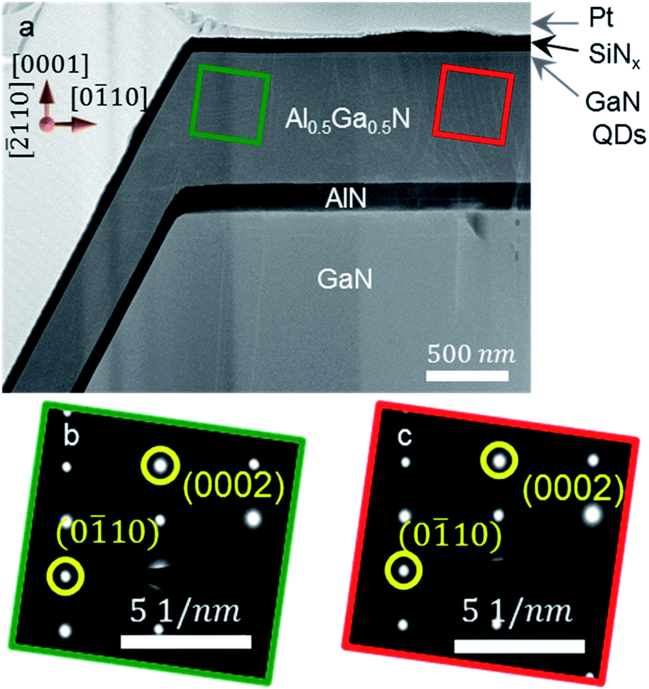 | ||
| Fig. 4 (a) Cross-sectional view HAADF STEM image taken near the boundary region of the truncated pyramid structure. (b and c) SAD pattern images of the AlxGa1−xN layers below B- and P-QDs, respectively. Note that the SiNx and Pt layers are deposited to protect the GaN QDs layers when preparing a STEM specimen. | ||
Furthermore, we found that the shape of B-QDs was elongated in the direction {100}, unlike P-QDs, i.e., the ratios between the major- and minor-axes of B- and P-QDs were 2.37 ± 1.19 and 1.29 ± 0.47, respectively (see Fig. S1†). This result also validates that the AlxGa1−xN layer at the boundary region was laterally stretched compared to the region at the top of the pyramid, i.e. the boundary region had a different strain state compared to the AlGaN region at the top of the pyramid, leading to a modification of the QD growth process and shape, as observed for the growth of GaN dots and wires on AlGaN (122) and (0001) surfaces.9,10
Fig. 5 shows the macro-PL spectra, time-resolved PL (TRPL) results, and panchromatic CL images as a function of temperature. From the measured lifetime and PL intensity change with temperature, we could extract out the radiative and nonradiative lifetimes as a function of temperature.22 The radiative lifetimes were 0.29, 0.35, and 0.56 ns for S-, B-, and P-QDs at 10 K, respectively. The radiative lifetime of S-QDs was faster than that of B- and P-QDs due to the negligible built-in electric field of the semipolar facet. We found that the radiative lifetime of B-QDs was faster than that of P-QDs, which also validates the reduction of the strain-induced piezoelectric field in B-QDs. With increasing temperature from 10 to 300 K, the radiative lifetimes (red lines in Fig. 5a–c) of S-, B- and P-QDs were nearly constant, indicating zero-dimensional exciton behavior.23 On the other hand, the non-radiative process (blue lines in Fig. 5a–c) became dominant near room-temperature since thermally activated excitons can be captured by defects, because the diffusion length is long enough.24
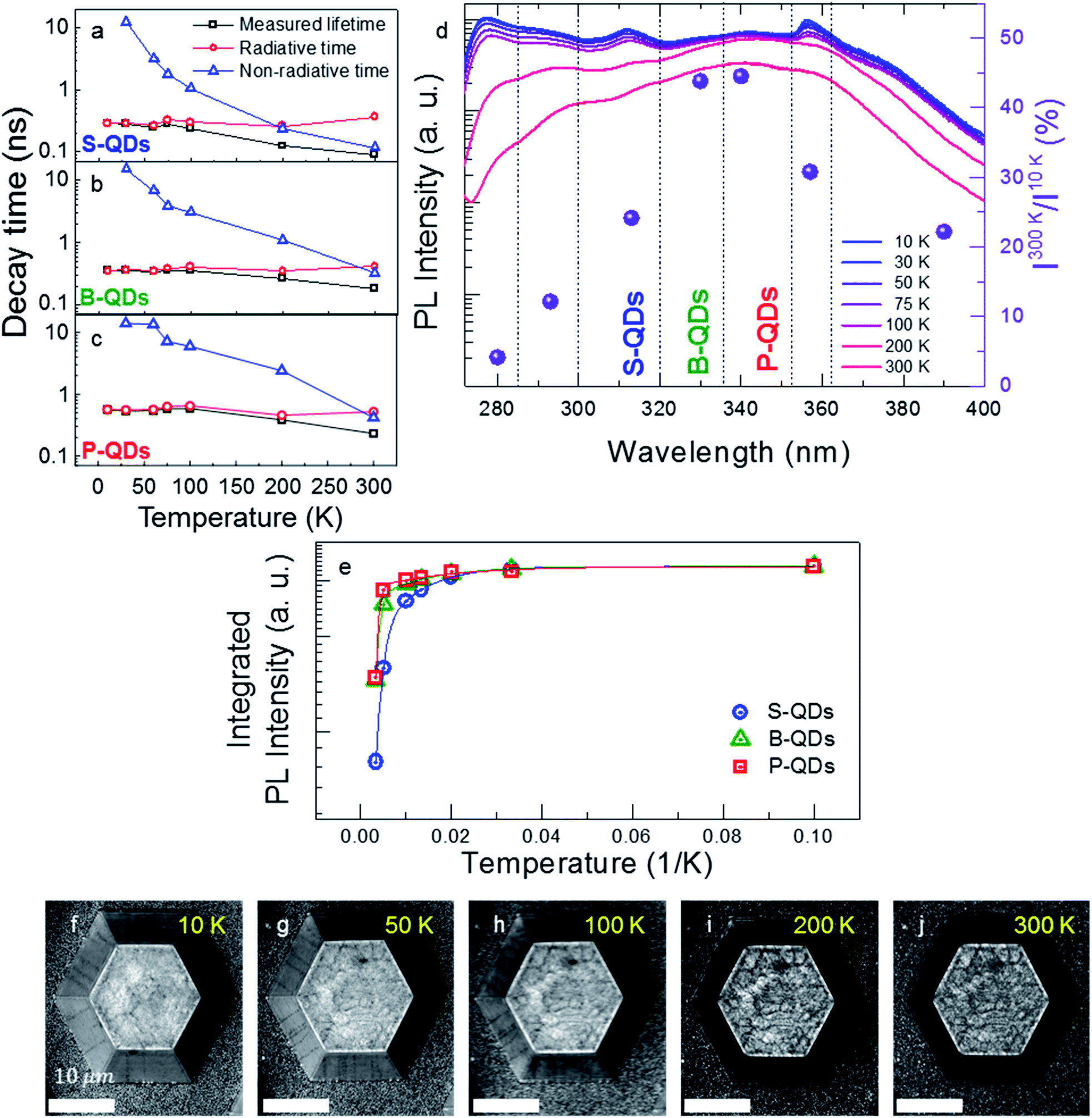 | ||
| Fig. 5 (a–c) Measured, radiative and non-radiative lifetimes of S-, B- and P-QDs as a function of temperature, respectively. (d) Temperature dependent PL spectra and intensity ratio between 10 and 300 K. (e) Integrated PL intensity of S-, B- and P-QDs as a function of temperature, respectively. (f–j) Temperature dependent panchromatic CL images. | ||
In general, the dislocation density on the c-plane of the truncated pyramid structure is much higher than that at a laterally over-grown semipolar facet.25 With elevating temperature, however, the non-radiative lifetime of S-QDs decreased faster than the others, and was nearly comparable to the radiative lifetime above 200 K, whereas the non-radiative lifetimes of B- and P-QDs were still longer than radiative lifetimes (compare the blue and red lines in Fig. 5a–c).
To quantitatively analyze the temperature-dependent carrier behavior, we investigated the temperature-dependent PL spectra and integrated PL intensity ratio between 10 and 300 K (I300 K/I10 K) as shown in Fig. 5d. I300 K/I10 K of the QDs is higher than that of the AlxGa1−xN matrix because the excited carriers or excitons at the AlxGa1−xN layers easily migrate into the QDs at higher temperature. However, we found that the I300 K/I10 K of S-QDs is smaller than that of P- and B-QDs. In other words, the PL intensity of S-QDs decreased when the temperature was above 200 K, which was consistent with the fast non-radiative lifetime of S-QDs (Fig. 5a). This indicates that the thermally activated excitons of S-QDs could be delocalized and escape into the GaN wetting layer or AlxGa1−xN layers. In previous work, the QDs’ height-dependent I300 K/I10 K was investigated.26 The I300 K/I10 K of smaller height QDs (ca. 1 nm) was lower than that of larger height QDs (ca. 2.3 nm), since the small height of QDs provides a reduced carrier localization potential (and a spreading of their wave functions in the barriers), resulting in less efficient carrier confinement at higher temperatures.26 In this respect, S-QDs would have weaker carrier localization than B- and P-QDs. We measured the integrated PL intensities (I) of S-, B- and P-QDs as a function of temperature (Fig. 5e), where the activation energy of QDs was estimated from an Arrhenius equation, I = I0(1 + A1e−E1/KBT + A2e−E2/KBT)−1, where E1 and E2 are referred to as the localization energy of shallow and deep localized states, respectively. In the high temperature regime, the escape behavior of thermally activated carriers is associated with A2 and E2, where A2 describes the proportion of non-radiative recombination centers.27,28 The fitting parameters of A1, A2, E1 and E2 for S-, B- and P-QDs are listed in Table 1. Since there exists high density of threading dislocations on the (0001) polar facet propagating from the GaN template,25 the proportion of non-radiative recombination centers at the polar facet can be much larger than that of the semipolar facet.25 It was evident that the A2 of P-QDs was about 10 times larger than that of S-QDs. For E2, we considered the energy difference of the valence band between the exciton transition energy of the GaN QDs and GaN wetting layer. Since the valence band offset of GaN/AlN is about 2.45 times lower than the conduction band offset,29 hole carriers would determine the activation energy for thermal escape behavior. In this respect, the energy difference of the valence band between the exciton transition energy of the GaN QDs and AlxGa1−xN layer was ∼136 meV (∼229 meV) for S-QDs (P-QDs). Although these values were not precisely identical to the E2 obtained from the Arrhenius equation, this strongly indicates that the low I300 K/I10 K of S-QDs was a result of weak carrier localization. In addition to the AlxGa1−xN layer, the thermally activated carriers could escape through the GaN wetting layer. The GaN wetting layer has a lower energy than AlxGa1−xN layers and behaves as a GaN quantum well layer sandwiched between two AlxGa1−xN layers.30,31 In Fig. 5d, the emission wavelength of the GaN wetting layer is not clearly distinguishable due to our broadband UV spectrum range. To clarify the emission wavelength of the GaN wetting layer, we obtained CL spectra using local excitation (see Fig. 5f–j). When local excitation was performed on the (0001) polar facet, the emission wavelength of P-QDs was clearly distinguished from that of the GaN wetting layer and AlxGa1−xN layer, which was consistent with our previous studies.8,10,20 On the other hand, the emission wavelengths of S-QDs and the GaN wetting layer were found to overlap with each other, which consequently indicated a reduced band offset between S-QDs and the GaN wetting layer. As a result, the thermal escape of carriers in S-QDs was attributed to the small band offset leading to a weaker confinement compared to P-QDs and a smaller I300 K/I10 K ratio even though the density of nonradiative recombination centers is reduced in this region.
| A 1 | E 1 (meV) | A 2 | E 2 (meV) | |
|---|---|---|---|---|
| S-QDs | 0.92 | 10.43 ± 0.66 | 45.21 | 74.79 ± 2.97 |
| B-QDs | 0.32 | 7.62 ± 1.02 | 88.11 | 114.87 ± 8.45 |
| P-QDs | 0.19 | 5.51 ± 2.50 | 581.75 | 162.63 ± 43.52 |
The thermal escape behavior of carriers was also observed in the temperature-dependent panchromatic CL images, as shown in Fig. 5f–j. A homogeneous panchromatic CL intensity was observed on the whole truncated pyramid structure at 10 K, whereas the panchromatic CL intensity at the semipolar facet was relatively reduced above 200 K. We expect that maintaining the broadband UV emission spectrum at high temperature above 200 K may be possible by adjusting the QD size26 and/or the surrounding AlGaN layer with higher Al contents or by introducing QD formation without the GaN wetting layer.7,32 Finally, we emphasize that our unique QD combination formed on truncated pyramid structures shows great promise for solid-state based broadband UV emitters, which would not only replace conventional arc-lamps but also expand their UV applications.
Experimental section
Optical characterization
CL (monoCL4, Gatan, Inc., Pleasanton, CA, USA) equipment connected to a SEM was used, where the used acceleration voltage was 5 kV. A transmission electron microscopy specimen was prepared using a focused ion beam (Helios nanolab 450 F1). High-resolution transmission electron microscopy (HRTEM, Titan cubed G2 60-300) was employed. The elastic strain was calculated using COMSOL Multiphysics based on the theory of continuum elasticity. For the optical characterization, macro-PL, PLE and TRPL setups with a cryostat were used in the temperature range from 10 to 300 K. The macro-PL was measured with 266 nm fourth-harmonic generation of a Nd:YAG pulsed laser. The PLE was measured using xenon-lamp light dispersed by a monochromator. The TRPL was measured using 266 nm third-harmonic generation of a pulsed-mode Ti:sapphire laser and a streak camera.Conclusions
In summary, by forming GaN QDs on GaN-based hexagonal truncated pyramid structures, we successfully demonstrated the broadband UV emission spectrum ranging from ∼400 nm (UV-A) to ∼270 nm (UV-C) with homogeneous intensity. We found that the built-in electric field and growth rate were different depending on the facets of pyramid structures. As a result, the emission wavelengths for QDs grown on each facet and at the facet edges were distinct, which provides the broad UV spectrum. In particular, although B- and P-QDs were grown on the same polar facet (0001), we found that the B-QDs have distinct optical and structural properties from P-QDs, due to the locally suppressed strain in the boundary region. From temperature-dependent PL and TRPL, we found that the thermally activated excitons in S-QDs were delocalized above 200 K, as a consequence of the smaller height of S-QDs. Such behavior could be suppressed by designing suitable QD active regions with adjusted growth conditions. This work presents a solid-state based broadband UV light source that could potentially replace arc-lamp-based applications.Conflicts of interest
There are no conflicts to declare.Acknowledgements
This work was supported by the National Research Foundation (NRF-2019R1A2B5B03070642) of the Korea government (MSIP), and Samsung Science and Technology Foundation under Project Number SSTF-BA1602-05. J. B., S. M., B. A. and M. L. acknowledge support from the ANR Project 〈ANR-14-CE26-0025〉 “NANOGANUV”, and also from GANEX (ANR-11-LABX-0014), which belongs to the publicly funded “Investissements d'Avenir” program managed by the French ANR agency.References
- H. Hirayama, S. Fujikawa, N. Noguchi, J. Norimatsu, T. Takano, K. Tsubaki and N. Kamata, Phys. Status Solidi A, 2009, 206, 1176–1182 CrossRef CAS.
- M. Kneissl, T. Kolbe, C. Chua, V. Kueller, N. Lobo, J. Stellmach, A. Knauer, H. Rodriguez, S. Einfeldt, Z. Yang, N. M. Johnson and M. Weyers, Semicond. Sci. Technol., 2011, 26, 014036 CrossRef.
- M. Asif Khan, Phys. Status Solidi A, 2006, 203, 1764–1770 CrossRef.
- D. Y. Kim, J. H. Park, J. W. Lee, S. Hwang, S. J. Oh, J. Kim, C. Sone, E. F. Schubert and J. K. Kim, Light: Sci. Appl., 2015, 4, e263 CrossRef CAS.
- Y.-H. Cho, H. S. Kwack, B. J. Kwon, J. Barjon, J. Brault, B. Daudin and L. S. Dang, Appl. Phys. Lett., 2006, 89, 251914 CrossRef.
- Y.-H. Cho, B. J. Kwon, J. Barjon, J. Brault, B. Daudin, H. Mariette and L. S. Dang, Appl. Phys. Lett., 2002, 81, 4934–4936 CrossRef CAS.
- J. Brault, S. Matta, T.-H. Ngo, M. Korytov, D. Rosales, B. Damilano, M. Leroux, P. Vennéguès, M. Al Khalfioui, A. Courville, O. Tottereau, J. Massies and B. Gil, Jpn. J. Appl. Phys., 2016, 55, 05fg06 CrossRef.
- M. Leroux, J. Brault, A. Kahouli, D. Maghraoui, B. Damilano, P. de Mierry, M. Korytov, J.-H. Kim and Y.-H. Cho, J. Appl. Phys., 2014, 116, 034308 CrossRef.
- A. Kahouli, N. Kriouche, J. Brault, B. Damilano, P. Vennéguès, P. de Mierry, M. Leroux, A. Courville, O. Tottereau and J. Massies, J. Appl. Phys., 2011, 110, 084318 CrossRef.
- J. Brault, T. Huault, F. Natali, B. Damilano, D. Lefebvre, M. Leroux, M. Korytov and J. Massies, J. Appl. Phys., 2009, 105, 033519 CrossRef.
- J. Brault, S. Matta, T.-H. Ngo, D. Rosales, M. Leroux, B. Damilano, M. A. Khalfioui, F. Tendille, S. Chenot, P. De Mierry, J. Massies and B. Gil, Mater. Sci. Semicond. Process., 2016, 55, 95–101 CrossRef CAS.
- W. M. Hikal and B. L. Weeks, J. Therm. Anal. Calorim., 2011, 110, 955–960 CrossRef.
- X. Zhu, K. Wang, J. Zhu and M. Koga, J. Agric. Food Chem., 2001, 49, 4790–4794 CrossRef CAS PubMed.
- T. Hommel and R. M. Szeimies, Photodiagn. Photodyn. Ther., 2017, 17, A14–A15 CrossRef.
- J. Takao, K. Ariizumi, I. I. Dougherty and P. D. Cruz Jr, Photodermatol., Photoimmunol. Photomed., 2002, 18, 5–13 CrossRef CAS PubMed.
- M. Korytov, M. Benaissa, J. Brault, T. Huault, T. Neisius and P. Vennéguès, Appl. Phys. Lett., 2009, 94, 143105 CrossRef.
- J.-H. Kim, B.-J. Kwon, Y.-H. Cho, T. Huault, M. Leroux and J. Brault, Appl. Phys. Lett., 2010, 97, 061905 CrossRef.
- S.-H. Lim, Y.-H. Ko, C. Rodriguez, S.-H. Gong and Y.-H. Cho, Light: Sci. Appl., 2016, 5, e16030 CrossRef CAS PubMed.
- T. Huault, J. Brault, F. Natali, B. Damilano, D. Lefebvre, L. Nguyen, M. Leroux and J. Massies, Appl. Phys. Lett., 2008, 92, 051911 CrossRef.
- S. Matta, J. Brault, T. H. Ngo, B. Damilano, M. Korytov, P. Vennéguès, M. Nemoz, J. Massies, M. Leroux and B. Gil, J. Appl. Phys., 2017, 122, 085706 CrossRef.
- S. Zhou, Y. Liu, D. Wang, Z. Yu, W. Zhao, L. Le and P. O. Holtz, Superlattices Microstruct., 2015, 84, 72–79 CrossRef CAS.
- J.-H. Kim, Y.-H. Ko, J.-H. Cho, S.-H. Gong, S.-M. Ko and Y.-H. Cho, Nanoscale, 2014, 6, 14213–14220 RSC.
- Y. H. Ko, J. H. Kim, L. H. Jin, S. M. Ko, B. J. Kwon, J. Kim, T. Kim and Y. H. Cho, Adv. Mater., 2011, 23, 5364–5369 CrossRef CAS PubMed.
- M. Kim, S. Choi, J. H. Lee, C. Park, T. H. Chung, J. H. Baek and Y. H. Cho, Sci. Rep., 2017, 7, 42221 CrossRef CAS PubMed.
- D. Zhu, D. J. Wallis and C. J. Humphreys, Rep. Prog. Phys., 2013, 76, 106501 CrossRef CAS PubMed.
- J. Brault, D. Rosales, B. Damilano, M. Leroux, A. Courville, M. Korytov, S. Chenot, P. Vennéguès, B. Vinter, P. De Mierry, A. Kahouli, J. Massies, T. Bretagnon and B. Gil, Semicond. Sci. Technol., 2014, 29, 084001 CrossRef.
- Y. Sun, Y.-H. Cho, H. M. Kim, T. W. Kang, S. Y. Kwon and E. Yoon, J. Appl. Phys., 2006, 100, 043520 CrossRef.
- Y.-H. Ko, J.-H. Kim, S.-H. Gong, J. Kim, T. Kim and Y.-H. Cho, ACS Photonics, 2015, 2, 515–520 CrossRef CAS.
- S. H. Wei and A. Zunger, Appl. Phys. Lett., 1996, 69, 2719–2721 CrossRef CAS.
- W. Yang, R. R. Lowe-Webb, H. Lee and P. C. Sercel, Phys. Rev. B: Condens. Matter Mater. Phys., 1997, 56, 13314–13320 CrossRef CAS.
- C. Lobo, R. Leon, S. Marcinkevicius, W. Yang, P. C. Sercel, J. Zou, X. Z. Liao and D. J. H. Cockayne, Phys. Rev. B: Condens. Matter Mater. Phys., 1999, 60, 16647–16651 CrossRef CAS.
- P. B. Joyce, T. J. Krzyzewski, G. R. Bell, B. A. Joyce and T. S. Jones, Phys. Rev. B: Condens. Matter Mater. Phys., 1998, R15981–R15984 CrossRef CAS.
Footnotes |
| † Electronic supplementary information (ESI) available. See DOI: 10.1039/d0na00052c |
| ‡ These authors equally contributed. |
| § Present address: R&D Investment Planning Team, Korea Institute of S&T Evaluation and Planning (KISTEP), Chungcheongbuk-do 27740, Republic of Korea. |
| This journal is © The Royal Society of Chemistry 2020 |