
 Open Access Article
 This Open Access Article is licensed under a Creative Commons Attribution-Non Commercial 3.0 Unported Licence
Multilevel nanoimprint lithography with a binary mould for plasmonic colour printing†
Muhammad Faris
Shahin Shahidan
 *a,
Jingchao
Song
a,
Timothy D.
James
b and
Ann
Roberts
a
*a,
Jingchao
Song
a,
Timothy D.
James
b and
Ann
Roberts
a
aSchool of Physics, The University of Melbourne, 3010, Australia. E-mail: mshahidan@student.unimelb.edu.au
bReserve Bank of Australia, Craigieburn, Victoria 3064, Australia
First published on 13th April 2020
Abstract
Pigment-free colouration based on plasmonic resonances has recently attracted considerable attention for potential in manufacturing and other applications. For plasmonic colour utilizing the metal-insulator-metal (MIM) configuration, the generated colour is not only dependent on the geometry and transverse dimensions, but also to the size of the vertical gap between the metal nanoparticles and the continuous metal film. The complexity of conventional fabrication methods such as electron beam lithography (EBL), however, limits the capacity to control this critical parameter. Here we demonstrate the straightforward production of plasmonic colour via UV-assisted nanoimprint lithography (NIL) with a simple binary mould and demonstrate the ability to control this gap distance in a single print by harnessing the nanofluidic behaviour of the polymer resist through strategic mould design. We show that this provides a further avenue for controlling the colour reflected by the resulting plasmonic pixels as an adjunct to the conventional approach of tailoring the transverse dimensions of the nanostructures. Our experimental results exhibit wide colour coverage of the CIE 1931 XY colour space through careful control of both the length and periodicity and the resulting vertical gap size of the structure during the nanoimprinting process. Furthermore, to show full control over the vertical dimension, we show that a fixed gap size can be produced by introducing complementary microcavities in the vicinity of the nanostructures on the original mould. This demonstrates a simple method for obtaining an additional degree of freedom in NIL not only for structural colouration but also for other industrial applications such as high-density memory, biosensors and manufacturing.
1 Introduction
Recently, the use of plasmonic nanostructures for structural colouration has received major attention due to their ability to selectively absorb and scatter light at characteristic wavelengths producing subtractive and non-diffractive colour. The advantages of plasmonic, rather than pigment-based, approaches to colouration include the capacity for single-step, high-resolution image printing at the diffraction limit,1 the ultrathin geometry of plasmonic devices, their mechanical and chemical robustness and stability,2 their relatively low toxicity and the reduced set of materials required facilitating the manufacturing process and subsequent recycling. These attractive properties have been studied for a wide range of applications such as colourimetric sensors, colour filters with subwavelength dimensions and colouration of consumer products.3–5 Plasmonic colouration originates in the strongly wavelength-dependent scattering and absorption of light which arises from the excitation of localised surface plasmon (LSP) resonances on the surface of sub-wavelength metallic nanoparticles and nanocavities.6 The resonances of the metal-insulator-metal (MIM) configuration (Fig. 1) where metallic nanoparticles embedded in a transparent dielectric ‘float’ above their Babinet complementary screen, are dependent not only on the transverse dimensions of the nanostructures,7–11 but also the size of the vertical gap (g) between the nanoantenna and the perforated backplane film. This vertical gap controls the particle-film coupling strength and, hence, the resulting colouration seen in reflection.12 While many approaches have been proposed to improve the functionality and quality of the resulting colouration, the key challenge remains controlling both the transverse and vertical dimensions of the nanostructures in a single nanofabrication process.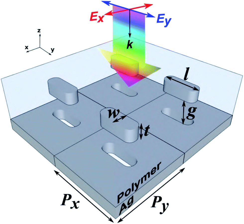 | ||
| Fig. 1 Schematic design of the plasmonic pixel comprising arrays of the ‘floating’ Ag nanorod and the complementary screen, arranged in a rectangular lattice. The nanorod has a length l, width w and thickness t. The array has periodicities in the x- and y-directions Px and Py, respectively, while the gap between the top of the metal film and the bottom of the Ag nanoparticle is g. Light, linearly polarized in either the x- or y-direction, is incident normally from the nanorod side, while the reflected light is collected from the same side of the sample. | ||
In previous studies, a grayscale technique involving electron beam lithography (EBL),13–15 focused ion beams (FIB) milling16 and photolithography (PL)17 have been utilised to produce nanostructures with varying vertical dimension (i.e. grayscale) for structural colouration and 3-dimensional plasmonic devices. The grayscale approach, however, require meticulous control of electrons, ions and photon dosage. Additionally, EBL and FIB have relatively low-throughput while PL produces structures with feature size limited to diffraction.18 Nanoimprint lithography (NIL),19 on the other hand, offers a rapid nanopattern replication process by means of mechanical transfer from mould onto a surface at minimal cost without compromising the nanoscale resolution.20 Due to these attractive features, different NIL techniques have been developed and are widely used for fabrication of various plasmonic devices.21,22 Previously, thermal NIL has been successfully demonstrated to produce high-resolution surfaces exhibiting plasmonic colour.1,23 A more industrial approach has been performed by Højlund et al. where thermal roll-to-roll nanoimprint lithography (R2R-NIL) was used to mass-produce devices exhibiting plasmonic colour.24 Thermal NIL, however, involves heating to high temperatures (typically around 150 °C, depending on the type of resist) which not only consumes energy but requires meticulous control over the relevant imprint parameters such as temperature and pressure. The UV-assisted NIL process, on the other hand, requires no heating and can be performed at room temperature and therefore, thermal damage, energy usage and process time can be minimized. Furthermore, the use of low viscosity photocurable resist requires a relatively low pressure (<4 bar) to emboss the structures, thus reducing potential damage to the mould.25 Despite the clear benefits of high-throughput, good quality pattern replication and plasmonic colour production there has been no discussion in the literature of any capacity of NIL to vary the vertical dimension, including the gap size in the MIM structure, across a sample using a simple, two-step (binary) mould.
The MIM structures considered here are fabricated using NIL into a resist followed by a single metallisation step. Since the resulting reflected colour produced by these devices is sensitive to the vertical gap size12 and this gap correlates directly with the imprint depth, the capacity to vary the imprint depth across a sample provides an additional degree of freedom in NIL-facilitated plasmonic colouration. During the nanoimprint process, the homogeneity of the imprint depth of the replicated structure is highly dependent on the resist filling behaviour in nanoscale cavities on the mould. The mould design (e.g. the size of the cavities, the density of structures and imprint area) is one of the significant factors affecting the resist filling process into cavities in the mould.25–32 Previous simulations of the NIL process performed by Yin et al. showed that an inhomogeneous imprint depth resulted when a mould composed of both micro- and nanoscale features was used for NIL due to variations across the sample in the resist filling rate.31 A similar effect was observed when a mould with various pattern densities was used in the NIL process.33 Although inhomogeneous imprint depth often caused unwanted artefact appearing in the NIL pattern transfer process34,35 we, on the other hand, find that this feature is an advantage when producing plasmonic colour as such it permits control over the vertical dimension and add another degree of freedom for colour tuning.
Here we demonstrate simple, scalable fabrication of multilevel plasmonic nanostructures via UV-assisted nanoimprint lithography (NIL) and the capacity to tune the colour of light reflected from the surface by controlling the vertical gap in the structure in a single print using a binary NIL mould with tailored pattern densities. In addition to experimentally demonstrating the role played by mould architecture in determining the imprint depth, we investigate the influence on resulting plasmonic colouration. The details of the building block of the MIM plasmonic pixel to be considered here is shown in Fig. 1. The structure comprises Ag nanorods with length varying from l = 75–150 nm and fixed width w = 50 nm, sitting above an aperture in a continuous Ag film with the same transverse dimensions. The nanoparticle is supported by the surrounding dielectric. The vertical gap, g between the particle and the metal film is determined by the imprint depth which, in turn, depends on the details of the resist filling process. The particles are arranged in a rectangular lattice with a fixed periodicity in the y-direction, Py = 300 nm, while the periodicity in the x-direction, Px is varied from 100–300 nm. The thickness of the particle and metal film is fixed at t = 50 nm. By varying the length, l and pitch size, Px of the structure, this generates not only plasmonic colour variations arising from tailored transverse feature sizes but also from the uneven vertical gap size across the imprinted structure resulting from variations in filling rate. Although the ability to vary the gap size of the structure in a single imprint with a simple binary mould is useful in some applications such as the surface colouration discussed here, this can be problematic in other applications. We, therefore, suggest a simple solution to avoid gap size variation in the sample by introducing a complementary microcavity mesh into the original mould architecture permitting filling-rate compensation in different pattern densities resulting in an almost constant gap size and thus the resonance wavelength.
2 Results and discussion
The plasmonic surface fabrication process involves three major stages with details provided in the Experimental section. Firstly, a silicon (Si) master mould is fabricated using electron beam lithography (EBL) for patterning on a Si wafer and further etched using reactive ion etching (RIE), producing arrays of rectangular nanoprotrusions of constant height across the mould. To produce a variation in the colour of the light reflected from the final plasmonic structure, both the length, l of the nanoprotrusions and the array periodicity in the x-direction, Px are tailored, thus creating a multidensity pattern on the mould (Fig. 2(a)). The fabrication of the mould using EBL is a ‘one-off’ process and the silicon mould can be cleaned and reused in multiple nanoimprinting processes. The second stage involve pattern replication using the UV-assisted nanoimprint lithography (UV-NIL) whereby the master mould is embossed onto a UV resist-coated glass substrate (Fig. 2(b)). The resist is cured under UV exposure while the pressure is maintained. This creates a negative of the mould with an imprint depth, hi that is a function of not only the height of the nanoprotrusions and the selected NIL parameters, but also the pattern density which affects the resist filling during the process. To complete the device fabrication, the replicated pattern was then coated with thin layer of silver (Ag) using electron beam evaporation, producing a nanoantenna array and its complementary perforated film (Fig. 2(c)).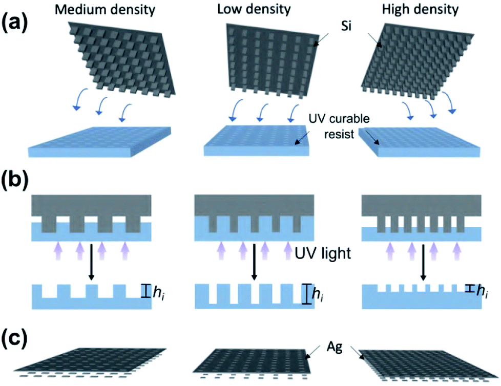 | ||
| Fig. 2 Schematics of the UV-assisted nanoimprint lithography (UV-NIL) process: (a) a master mould consist of multiple density of nanoprotrusions used in the UV-NIL which results in the nanocavity with various imprinting depth, hi as depicted in (b). (c) Scheme showing the geometry of the Ag ‘floating’ resonance particle and metal back layer upon metal coating process. Height of the structures in the schematics are not to be scaled. | ||
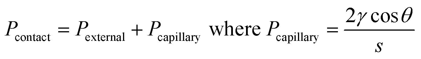
SEM images in Fig. 3 show the nanocavities on the imprinted sample (a–c) with varying lengths and periodicities. The morphology of the final fabricated structures are in very good agreement with their transverse counterparts on the mould, depicting excellent fidelity of the pattern replication (also refer Fig. S1†). Insets in Fig. 3(a–c) show white light optical microscope images taken in reflection of devices after metal coating. A variation in resulting colour is apparent. Cross-sectional images in Fig. 3(d–f) reveal that increasing the periodicity leads to a larger imprint depth, hi during the imprint process. This results in a shift in the resonance wavelength and, hence, the colour of the final structure even if other parameters are held fixed. The variation in imprint depth (and the resulting value of g, where g = hi − t) is mainly affected by the nanofluidic channelling behaviour of the resist during the NIL process.25,31,36 There are two major factors that influence the nanofluidic dynamics of the resist: (i) the architecture of the mould and (ii) the physical properties of the resist. For a given resist, the details of the mould architecture can be used to tune the behaviour of the gap size across the imprinted structure. Our results show that the film-nanoantenna vertical gap size, g has an approximately linear relationship to the periodicity, Px as depicted in the plot in Fig. 3(g) (see also Table S1† for detailed analysis of the line fitting). Inset (i) in Fig. 3(g) shows the cavity-filling mechanism of the resist during imprinting, where the dynamics of the liquid phase resist depend on the contact forces between the mould and resist. Contact force is expressed as the combination of external and capillary forces:31
 | (1) |
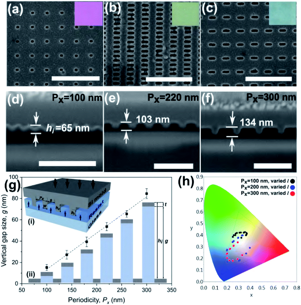 | ||
| Fig. 3 SEM images shows morphologies of the imprinted cavities of various length, l and periodicities, Px namely (a) l = 75 nm, Px = 300 nm; (b) l = 150 nm, Px = 100 nm and (c) l = 150 nm, Px = 300 nm. Insets shows colours generated by the corresponding structures. Cross-sectional images of nanocavities with length of 150 nm reveals the imprint depth of (d) hi = 65 nm, (e) hi = 103 nm and (f) hi = 134 nm for structure with periodicities of Px = 100 nm, Px = 220 nm and Px = 300 nm, respectively. All scale bars refer to 500 nm. (g) Plot shows relationship between the periodicity, Px and the vertical gap size, g. Inset: (i) schematic shows mechanism of resist flow during imprinting process where w and hc is the width and height of the nanoprotrusion, s is the cavity size and hi is the imprint depth, (ii) illustration shows post-metal deposition structure (metal thickness of t) with varying vertical gap size. (h) Position of the resultant colours on CIE 1931 XY colour space produced due to variation in periodicities and lengths of the nanorods. Namely, the black, blue, red dots indicate the colour positions in the CIE space obtained by varying l from 75–150 nm, and Px = 100, 200, 300 nm respectively. | ||
For a feature-rich mould composed of various cavity sizes, the resist filling rate can vary greatly across the mould due to the non-uniform distribution of contact force.31 The pitch size of the nanostructures influences the volume of cavity to be filled by the resist (inset (i) Fig. 3(g)). As the pattern density increases (decreasing periodicities), the resist fills a smaller cavity volume at a slower rate due to the higher viscous resistance, according to the Poiseuille law.37 This produces a shallower imprint depth, hi leading to a smaller film/nanorod gap size, g after metallization as illustrated in inset (ii) of Fig. 3(g). The change in the length of the nanostructure however, introduce a relatively smaller change in the cavity size thus results in a minimum variation to the imprint depths a shown in Fig. S2.† The results of a repeatability test with imprint results given in Fig. S3† indicate that the process is capable of reproducing the same colour palette even after multiple imprints. It also demonstrates that colour variations are not due to random defects occurring during the imprint process. The experimental results exhibit a wide colour coverage in the CIE 1931 XY colour space generated by varying length (l) and periodicity (Px) and subsequent vertical gap size, g as shown in Fig. 3(h).
Fig. 4(a–c) show experimentally-obtained two-dimensional reflectance spectra acquired from selected plasmonic pixels with varying periodicity, Px and vertical gap size, g, at three nanoparticle lengths i.e. l = 120 nm, 85 nm and 75 nm respectively. The measured reflectance exhibits two minima at shorter and longer wavelengths. For each nanoparticle size, these resonance wavelengths can be tuned by varying the periodicity parallel to the short-axis of the nanorods, Px, and the associated gap size g. To further understand features in the reflectance spectrum, Finite Element Method (FEM) simulations were performed where the periodicity, the length and vertical gap size of the structure were varied as in the experiments where the geometry was obtained from SEM images. The simulated 2D reflectance plots as a function of periodicity in Fig. S4† shows comparable trends in the location of features in the reflectance spectrum (depicted by the dashed lines) as obtained in experiments (Fig. 4(a–c)). The simulations show that for structures with periodicities less than 220 nm, the resonance due to the plasmonic coupling between adjacent nanoantennas38 results in the excitation of a higher-order resonance (a quadrupole mode) as depicted by the charge density distribution (inset (i) in Fig. 4(d)). This is accompanied by the appearance of an additional resonance, a quadrupole mode, at a shorter wavelength. At larger periodicities (Px ≥ 220 nm), the coupling strength between neighbouring nanoantennas becomes weaker as the separation increases (inset (ii) in Fig. 4(d)). This leaves only the lower-order dipole mode that resonates at longer wavelengths. On the other hand, previous work12 has shown that when the ‘floating’ nanoantenna is located at the optimal distance from the metal film, (equal to (2m + 1)λ/4, where m is an integer and λ is wavelength in the medium) the resulting structure exhibits the strongest resonance (inset (iii) in Fig. 4(d)). A slight increase in the gap size between the nanoantenna and the film within the near-field distance therefore significantly blue-shifts the wavelength of the dipole mode as a result of weaker plasmonic coupling between film and nanoantenna as depicted in inset (iv) in Fig. 4(d). Simulations assuming a structure with a fixed vetical gap size shown in Fig. S5,† however, show either no shift or a red-shift of the dipole mode thus confirming that the blue-shift in resonance wavelengths shown in Fig. 4(a–c) is due to increasing vertical gap size, g.
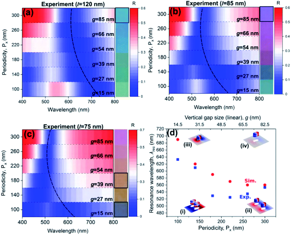 | ||
| Fig. 4 (a–c) Measured reflectance plot as function of periodicity, Px and vertical gap size, g for fixed length of nanorod l = 120, 85 and 75 nm respectively. Dashed line indicate blue-shift of the resonance wavelength (dipole mode). Insets shows the corresponding colours for each dimensions while colours in black boxes refers to cyan, magenta, yellow and black (CMYK) colours. (d) Plot shows relation between periodicities, Px, vertical gap size, g (obtained from linear relation shown in Fig. 3(g)) and resonance wavelengths, λres (dipole mode) for nanorod of length of 85 nm. Insets are the charge density distribution diagram depicting resonance mode and plasmonic coupling strength at (i) shorter and (ii) longer periodicity; and (iii) shorter and (iv) longer gap sizes. | ||
Optical images in the insets of Fig. 4(a–c) show colours of various hue and saturation seen in reflection from the structure with varying transverse and vertical dimensions. Here, we have demonstrated that by optimising the length and the vertical gap size via tailoring the particle spacing, we were able to produce cyan, magenta, yellow and black (CMYK) fundamental colours (colours in black boxes in inset of Fig. 4(a–c)). The colouration is strongly dependent on the excitation of the quadrupole and dipole mode of the structure. For example, both cyan (inset Fig. 4(a)) and magenta (inset Fig. 4(b)) colours were produced by adjusting the length of the nanorod to 120 nm (cyan) and 85 nm (magenta), while the periodicity was fixed at 300 nm and the vertical gap size at 85 nm. Decreasing the periodicity, Px, however, results in a change in the saturation and hue of the reflected colour due to a blue-shift of the dipole mode resonance and the broadband absorption contributed by both dipole and quadrupole mode. A yellow plasmonic pixel (inset Fig. 4(c)) was composed of nanorods with a length, l = 75 nm, periodicity, Px = 180 nm and vertical gap size, g = 39 nm. Similarly, by simply reducing the periodicity, Px and vertical gap size, g to 100 nm and 15 nm respectively, while maintaining the nanorod length at 75 nm, results in broadband absorption resulting from the excitation of both modes thus producing ‘black’ (inset Fig. 4(c)). The plot in Fig. 4(d) shows the resonance wavelength (dipole mode) as function of periodicity, Px, vertical gap size, g (obtained from the straight line fit of Fig. 3(g)) for devices with nanorods of length, l = 85 nm. The plot indicate that the resonance wavelength (dipole mode) is blue-shifted when the periodicity and vertical gap size increases. Discrepancies between the measured and simulated reflectance spectra may be due to the presence of the metal deposited on the sidewalls.39–41 This appearance of these artefacts could be minimized by producing nanocavities with more ideally rectangular profiles which is a challenge when using NIL. Some sidewall deposition should be expected as a result of the trapezoidal geometry of the nanocavities and the surface chemistry between the metal and the polymer resist film.41 In specific applications, balancing performance and scalability requires accommodating these defects in the design process. On the other hand, increasing the length of the rods results in a red-shift of the resonance wavelength as indicated by the position of the dashed line in Fig. 4(a–c) (see also Fig. 5(c and d)). Our approach, therefore, permits fine tuning of the position of the resonance wavelengths to produce a broad colour palette enabled by varying the transverse and vertical dimension.
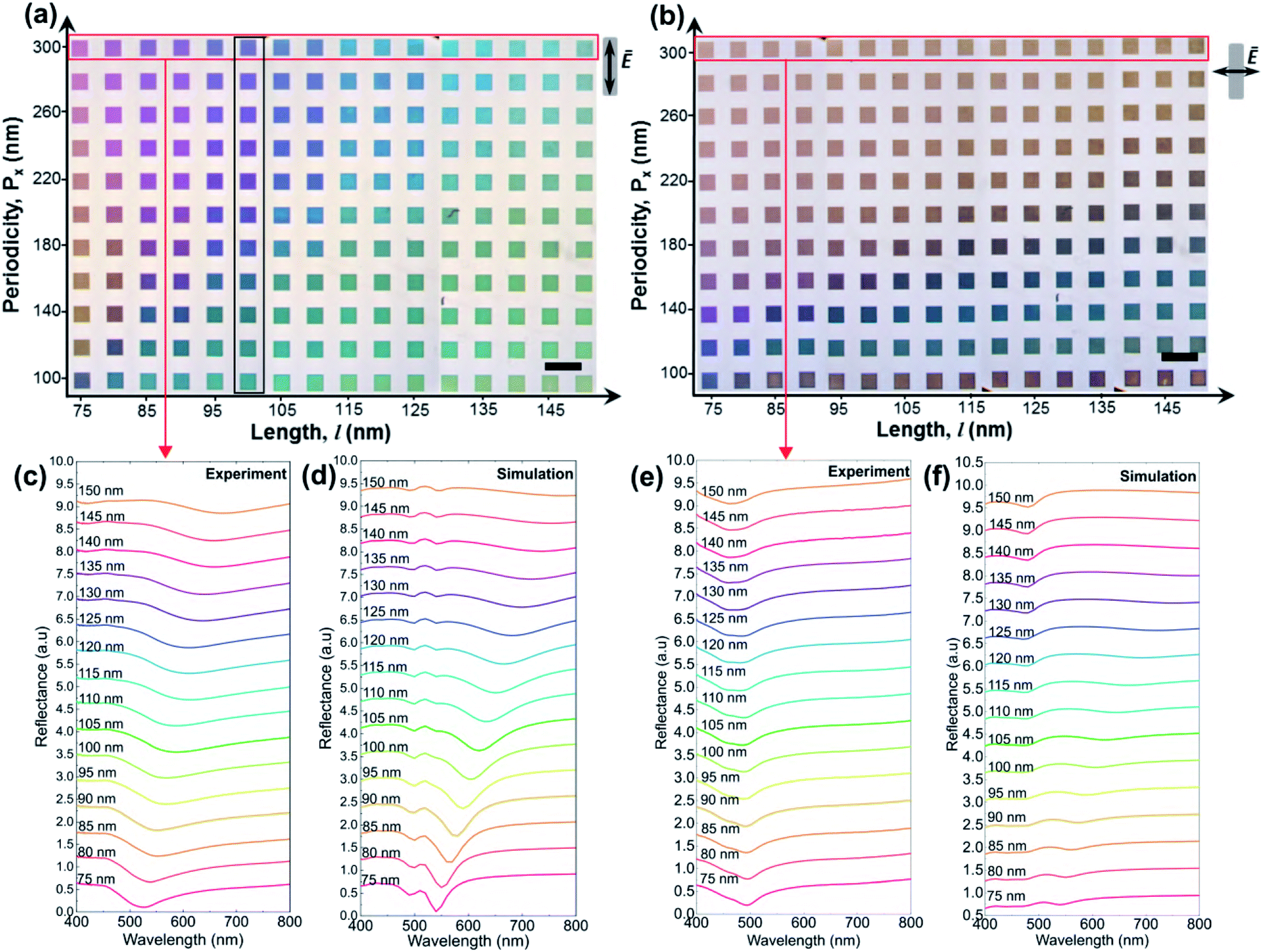 | ||
| Fig. 5 Bright-field optical micrograph of the colour palettes generated from the nanoimprinted samples under linearly polarised light with direction (a) parallel and (b) perpendicular to the long-axis of the nanorods. Structures in the red boxes have varying length, l and fixed periodicity, Px = 300 nm, while structures in the black box have varying periodicities, Px and fixed length, l = 100 nm. Scale bar refer to 0.4 mm. Corresponding reflectance spectra obtained from experiment and simulation of nanorod with fixed Px = 300 nm and l = 75–150 nm under polarization direction (c and d) parallel and (e and f) perpendicular to the long-axis of the rod (insets) respectively. The width, w is fixed at 50 nm. | ||
Optical images obtained in reflection with a bright field microscope and accompanying reflectance spectra were obtained across a range of pixel geometries to investigate their optical response. Fig. 5 shows optical micrographs of the entire colour palette with an imprinted area of 0.6 × 0.4 cm2 obtained when the structure was illuminated with linearly polarized light with electric field either parallel (Fig. 5(a)), or perpendicular to the long-axis (Fig. 5(b)), of the nanorods. The columns of the palettes correspond to changes in length, l, ranging from 75 nm to 150 nm in 5 nm increments, while the rows represent different periodicities, Px, ranging from 100 nm to 300 nm in 20 nm increments. The colours are clearly sensitive to the direction of polarisation due to the asymmetric shape of the nanorod. Colour variations were quantified by experimental reflection spectra obtained for nanorods with varying lengths, l but fixed periodicity, Px = 300 nm (red box). Since the structures in the red box have the same periodicity they also have approximately the same vertical gap size, g = 85 nm (refer Fig. 3(f)). The measured reflectance spectra in Fig. 5(c) shows that when the direction of polarisation is parallel to the long-axis of the rod, the resonance red-shifts as the length increases from 75 nm to 150 nm creating distinct colour changes. For example, a pixel appears magenta when the nanorod has a length of 80 nm, but cyan when the length is 130 nm (red box in Fig. 5(a)). Using the measured gap size obtained from fabricated devices, the simulated spectra also show comparable trends in the corresponding measured spectra as l increases (Fig. 5(d)), consistent with the trend observed elsewhere.7,12 In comparison, the resonance shift resulting from the change in periodicity shown previously in Fig. 4 resulted in a significant impact on the associated plasmonic colouration as can be seen in the colour variations in the black box of Fig. 5(a). In contrast to the case where the polarization is parallel to the long axis of the nanorods, the colours obtained for the orthogonal polarization show minimal variation with length as the width, w, was held fixed at 50 nm (red box in Fig. 5(b)). The measured reflectance spectra in Fig. 5(e) confirm that the position of the resonance minima barely changes as the length of the rods is increased. The simulated results in Fig. 5(e) are also in good agreement with the measured spectra.
Although we have demonstrated that a variable imprint depth provides an additional degree of freedom in creating plasmonic colouration, in many applications this can be undesirable. Several approaches have been proposed to reduce the global variation of imprint depth such as increasing the applied pressure,42 increasing the imprinting time,31,43 introducing additional microcavities or protrusions in proximity to the original design33 and utilising a cavity-equalized mould.36 To address this issue, we propose the addition of a novel mesh-like microcavity architecture to the multi-density mould to facilitate resist flow. The structure considered here has microcavities with a width, smicro = 5 μm and periodicity of 25 μm (schematic shown in Fig. 6(a)). The additional microcavities promote a more uniform distribution of resist by aiding the long-range transport of resist over various pattern densities.44 At the same time, the resist travels locally into the microstructure to assist cavity filling into the nanostructure in order to compensate and stabilise the filling rate as depicted in Fig. 6(a).31 This permits an almost constant resist filling rate over the sample producing a consistent imprint depth and resulting gap size in the final structure. Fig. 6(b) shows the top-view of the mould with mesh-like cavities, dividing the pixel into sub-pixels. Cross-sectional images in Fig. 6(c–e) reveal that cavities with almost the same imprint depth were produced regardless of the size of the lattice period through the use of this strategy. Fig. 6(f) shows the measured reflectance from the metallized nanoimprinted plasmonic pixels using the mould without (dotted lines) and with the microcavity mesh (solid lines), for nanorods with lattice periodicities, Px = 100 nm, 200 nm and 300 nm. As seen previously, the reflectance spectra exhibits a significant shift in the resonance minimum with increasing periodicity in the absence of the microcavities. In contrast, the spectra in Fig. 6(f) show no obvious resonance shift with additional microcavities since the gap (Fig. 6(e)) has a constant size. There is, however, a reduction in the depth of the reflectance minima as the periodicity increases due to a decrease in structure density. Ongoing work is aimed at optimizing the mesh to ensure uniform print depth while maximising particle density. Our results show that the mesh-like sub-pixel design is not only applicable to the generation of plasmonic colouration but can useful for other NIL processes to control imprint depths when utilizing a mould with a pattern of various densities.
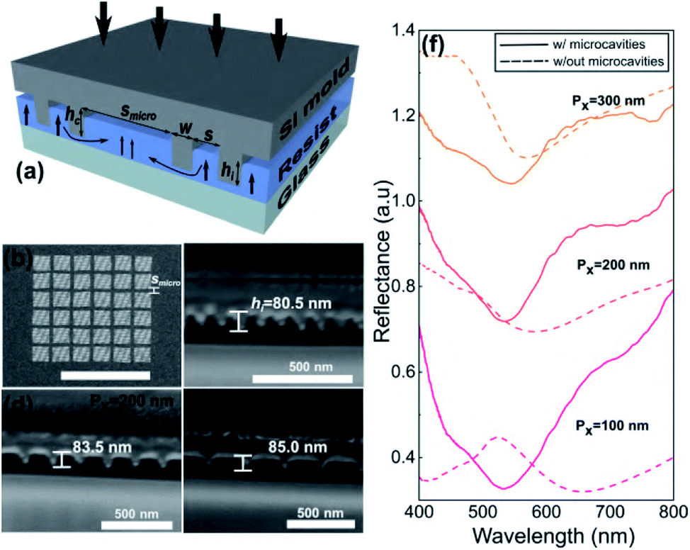 | ||
| Fig. 6 (a) Schematic shows resist dynamics during imprinting utilising mould with additional microcavity. (b) SEM image shows top-view of the mould design with additional microcavity mesh superimposed on the original pattern. Scale bar refers to 0.1 mm. Cross-sectional images reveals the imprint depth of (c) h = 80.5 nm, (d) h = 83.5 nm and (e) h = 85.0 nm for structure with periodicities, Px of 100 nm, 200 nm and 300 nm. (f) The measured reflectance of the colours fabricated using design without microcavity (dotted line) and with microcavity (solid line), for nanorod with length of l = 100 nm and lattice periodicities of Px = 100, 200, 300 nm. | ||
3 Conclusions
In conclusion, we demonstrate control over plasmonic coupling between film and nanoantenna using a specifically designed two-step NIL mould in a single print to produce wide-gamut plasmonic colouration. Our process is repeatable and shows that the coupling distance can be tailored by tuning the cavity volume of the mould. In the case where the array pitch affects the vertical gap size between the film and the nanorod, our results show that the resonance is not only sensitive to the length of the nanorods but also to the periodicity, Px of the arrays and the corresponding coupling distance i.e. vertical gap size, thus producing wide-gamut polarization-dependent plasmonic colour palettes. Alternatively, in the case where additional mesh-like microcavities are introduced adjacent to each subpixel, the filling rate of the resist throughout the sample is compensated regardless of pattern density. Consequently, there was no observable variation in the size of the gap between the top particle and bottom metal layer across the sample, and the resulting colour remains almost constant with periodicity. Our results demonstrate a novel approach to tailoring the resist filling mechanisms in multi-density moulds during NIL processes. This is particularly important for production of plasmonic devices which require nanoscale precision across surfaces orders of magnitude larger. From a fabrication point-of-view introducing a microcavity structure into the mould, suggests a simple solution to a longstanding issue in NIL. Future work involves an investigation of how the depth can be controllably varied across the pattern by modifying the compensating mesh across the mould and optimizing the relationship between the mesh design and colour brightness.4 Experimental
4.1 Master mould fabrication
Rectangular nanoprotrusions of 160 nm height with varying length (l) from 75 nm to 150 nm and periodicity in x direction (Px) from 100 nm to 300 nm were fabricated on the surface of a polished 4-inch Si master wafer using electron beam lithography (EBL), using 110 nm thick PMMA A4 film (MicroChem) as a positive resist. After exposure and development, 50 nm of Al was deposited as a masking layer for the etching process using deep reactive ion etching (DRIE). Post-etching process produces 160 nm height nanoprotrusions. The wafer was then cleaved into 2 cm smaller piece to match the size of the substrate.4.2 Sample fabrication
The UV curable resist was spun coated on the glass substrates at 1000 rpm. A 100 nm thick of underlayer resist (NXR-3023, Nanonex) was spun-coated onto the surface of cleanroom grade glass slides as an adhesion layer before soft-baked at temperature of 160 °C for 3 minutes to let the solvent evaporate. The UV curable resist (NXR-2030, Nanonex) was then spin-coated twice, layer-by-layer, producing an approximately 200 nm thick film. Prior to the nanoimprinting process, the mould was deposited via vapor phase deposition with a layer of trichlorosilane layer as an anti-adhesive layer. The pattern replication was performed using the NX B200 NIL tool from Nanonex. The mould was pressed on the glass substrate by air cushions at a pressure of 50 psi for 3 minutes. The resist was then cured under UV exposure for 40 seconds. The demoulding process was performed manually using a razor blade. The imprinted samples were subsequently deposited with 2 nm of Ge as adhesion layer and 50 nm of Ag film using electron beam evaporation at a rate of 0.05 nm s−1.4.3 Characterization
The FIB-SEM images shown in Fig. 4 and 5, were obtained with a FEI Helios NanoLab 600 Dual BeamSystem. Firstly, a 400 nm layer of platinum (Pt) was deposited on the structures to protect the soft surface and increase the conductivity. A low electron current at 43 pA was used for SEM imaging through the whole process. FIB milling was performed at 52° stage tilt (perpendicular to the ion beam). Both standard cross-section and cleaning cross-section with Ga ions were used for patterning. Subsequently, the cross-section SEM images were taken at 52° stage tilt.4.4 Optical measurements
Optical image of the patterned surfaces were obtained using a Nikon N1 camera attached to an optical microscope (Olympus BX60). A rotating linear polarizer located in the path of the light source was used select the linear polarization state thus showing the colour switch with direction of polarization. The reflectance spectra were obtained with a custom built optical cage setup. A broadband halogen lamp (HL-2000-FHSA, Mikropack) was used as a light source. Unpolarized light passed through the first objective lens with NA = 0.15 (10x UPlan, Nikon) and the calcite linear polarizer (GTH5M, Thorlabs), producing a collimated and linearly polarized light beam. The polarized light passed through the second objective lens of NA = 0.5 (20x UPlanFl, Nikon) before illuminating the sample. The light reflected from the sample was split by the first and second 50/50 non-polarising beam splitter cubes (CCM1-BS013, Thorlabs) to a USB CMOS camera (DCC1645C, Thorlabs) and calibrated spectrometer (QE6500, Ocean Optics Inc.). Reflectance spectra were obtained from the nanoparticle side of the resulting structures to optically characterise the samples.4.5 Simulations
The three-dimensional simulations of nanostructure models shown in this work were performed using the Finite Element Method (FEM) implemented in the Wave Optics module of COMSOL Multiphysics 5.4. Periodic boundary conditions were used on the sides of the unit cell. The material data for Ag was obtained from ref. 32 by Rakic et al. A mesh with maximum element size of 15 nm was used in detailed areas such as the nanorods and nanoaperture. Reflectance spectra were calculated using normal incidence port excitation of a plane wave linearly polarized either parallel or perpendicular to the long-axis of the rods and the reflectance calculated from the S-parameter |S11|2. Another port on the rear surface of the model prevented reflections back into the model. The refractive index of the resist and glass were both assumed to be n = 1.45.Conflicts of interest
There are no conflicts to declare.Acknowledgements
This research was supported by the Australian Research Council through LP160100054. This work was performed in part at Melbourne Center for Nanofabrication (MCN) in the Victorian Node of the Australian National Fabrication Facility (ANFF). Part of this work was also performed at Advanced Technologies Centre (ATC) in Swinburne University of Technology. We also thank Professor Paul Mulvaney and Dr Timothy J. Davis for their useful discussions.Notes and references
- K. Kumar, H. Duan, R. S. Hegde, S. C. W. Koh, J. N. Wei and J. K. W. Yang, Nat. Nanotechnol., 2012, 7, 557–561 CrossRef CAS PubMed.
- Y. Gu, L. Zhang, J. K. W. Yang, S. P. Yeo and C.-W. Qiu, Nanoscale, 2015, 7, 6409–6419 RSC.
- A. Choe, J. Yeom, R. Shanker, M. P. Kim, S. Kang and H. Ko, NPG Asia Mater., 2018, 1, 912–922 CrossRef.
- D. Fleischman, K. T. Fountaine, C. R. Bukowsky, G. Tagliabue, L. A. Sweatlock and H. A. Atwater, ACS Photonics, 2019, 6, 332–338 CrossRef CAS.
- A. Kristensen, J. K. W. Yang, S. I. Bozhevolnyi, S. Link, P. Nordlander, N. J. Halas and N. A. Mortensen, Nat. Rev. Mater., 2016, 2, 16088 CrossRef.
- I. Freestone, N. Meeks, M. Sax and C. Higgitt, Gold Bull., 2007, 40, 270–277 CrossRef CAS.
- X. M. Goh, Y. Zheng, S. J. Tan, L. Zhang, K. Kumar, C. W. Qiu and J. K. Yang, Nat. Commun., 2014, 5, 5361 CrossRef CAS PubMed.
- R. Mudachathi and T. Tanaka, Sci. Rep., 2017, 7, 1199 CrossRef PubMed.
- A. S. Roberts, A. Pors, O. Albrektsen and S. I. Bozhevolnyi, Nano Lett., 2014, 14, 783–787 CrossRef CAS PubMed.
- M. Miyata, H. Hatada and J. Takahara, Nano Lett., 2016, 16, 3166–3172 CrossRef CAS PubMed.
- J. R. Fan, W. G. Wu, Z. J. Chen, J. Zhu and J. Li, Nanoscale, 2017, 9, 3416–3423 RSC.
- T. D. James, P. Mulvaney and A. Roberts, Nano Lett., 2016, 16, 3817–3823 CrossRef CAS PubMed.
- Z. Yang, Y. Chen, Y. Zhou, Y. Wang, P. Dai, X. Zhu and H. Duan, Adv. Opt. Mater., 2017, 5, 1700029 CrossRef.
- Y. Wang, M. Zheng, Q. Ruan, Y. Zhou, Y. Chen, P. Dai, Z. Yang, Z. Lin, Y. Long and Y. Li, et al. , Research, 2018, 2018, 8109054 Search PubMed.
- K. Wilson, C. A. Marocico, E. Pedrueza-Villalmanzo, C. Smith, C. Hrelescu and A. L. Bradley, Nanomaterials, 2019, 9, 963 CrossRef CAS PubMed.
- Y. Chen, X. Yang and J. Gao, Light: Sci. Appl., 2019, 8, 1–9 CrossRef CAS PubMed.
- C. Williams, G. S. Gordon, T. D. Wilkinson and S. E. Bohndiek, ACS Photonics, 2019, 3132–3141 CrossRef CAS PubMed.
- W. Huang, X. Yu, Y. Liu, W. Qiao and L. Chen, Frontiers of Mechanical Engineering, 2017, 12, 99–109 CrossRef.
- S. Y. Chou, P. R. Krauss and P. J. Renstrom, J. Vac. Sci. Technol., B: Microelectron. Nanometer Struct.--Process., Meas., Phenom., 1996, 14, 4129–4133 CrossRef CAS.
- L. J. Guo, Adv. Mater., 2007, 19, 495–513 CrossRef CAS.
- A. Cattoni, P. Ghenuche, A.-M. Haghiri-Gosnet, D. Decanini, J. Chen, J.-L. Pelouard and S. Collin, Nano Lett., 2011, 11, 3557–3563 CrossRef CAS PubMed.
- A. Boltasseva, J. Opt. A: Pure Appl. Opt., 2009, 11, 114001 CrossRef.
- B. R. Lu, C. Xu, J. Liao, J. Liu and Y. Chen, Opt. Lett., 2016, 41, 1400–1403 CrossRef CAS PubMed.
- E. Højlund-Nielsen, J. Clausen, T. Mäkela, L. H. Thamdrup, M. Zalkovskij, T. Nielsen, N. Li Pira, J. Ahopelto, N. A. Mortensen and A. Kristensen, Adv. Mater. Technol., 2016, 1, 1600054 CrossRef.
- J. Taniguchi, Y. Kamiya, T. Ohsaki and N. Sakai, Microelectron. Eng., 2010, 87, 859–863 CrossRef CAS.
- A. Francone, PhD thesis, Institut National Polytechnique de Grenoble-INPG, 2010.
- H. Schift, J. Vac. Sci. Technol., B: Microelectron. Nanometer Struct.--Process., Meas., Phenom., 2008, 26, 458–480 CrossRef CAS.
- K.-D. Kim, H.-J. Kwon, D.-g. Choi, J.-H. Jeong and E.-s. Lee, Jpn. J. Appl. Phys., 2008, 47, 8648 CrossRef CAS.
- S. Gilles, M. Meier, M. Prömpers, A. v. d. Hart, C. Kügeler, A. Offenhäusser and D. Mayer, Microelectron. Eng., 2009, 86, 661–664 CrossRef CAS.
- K. Ishibashi, H. Goto, J. Mizuno and S. Shoji, J. Nanotechnol., 2012, 2012, 1–9 CrossRef.
- M. Yin, H. Sun and H. Wang, Micromachines, 2018, 9, 335 CrossRef PubMed.
- Y. Hirai, J. Photopolym. Sci. Technol., 2010, 23, 25–32 CrossRef CAS.
- H. Hiroshima, Microelectron. Eng., 2009, 86, 611–614 CrossRef CAS.
- S. Sreenivasan, Microsyst. Nanoeng., 2017, 3, 17075 CrossRef CAS PubMed.
- Q. Wang, H. Hiroshima, H. Atobe and S.-W. Youn, J. Vac. Sci. Technol., B: Nanotechnol. Microelectron.: Mater., Process., Meas., Phenom., 2010, 28, C6M125–C6M129 CAS.
- S.-W. Youn, K. Suzuki and H. Hiroshima, Jpn. J. Appl. Phys., 2018, 57, 06HG03 CrossRef.
- J. Cai and W.-D. Li, 2018, arXiv preprint arXiv:1811.05103.
- S. D. Rezaei, J. Ho, R. J. H. Ng, S. Ramakrishna and J. K. W. Yang, Opt. Express, 2017, 25, 27652–27664 CrossRef CAS PubMed.
- S. Murthy, H. Pranov, N. A. Feidenhans, J. S. Madsen, P. E. Hansen, H. C. Pedersen and R. Taboryski, Nanoscale, 2017, 9, 14280–14287 RSC.
- P. Dai, Y. Wang, X. Zhu, H. Shi, Y. Chen, S. Zhang, W. Yang, Z. Chen, S. Xiao and H. Duan, Nanotechnology, 2018, 29, 395202 CrossRef PubMed.
- S. Goetz, M. Bauch, T. Dimopoulos and S. Trassl, Nanoscale Adv., 2020, 2, 869–877 RSC.
- H. Lee, J. Vac. Sci. Technol., B: Microelectron. Nanometer Struct.--Process., Meas., Phenom., 2005, 23, 1102–1106 CrossRef CAS.
- M. Yin, H. Sun and H. Wang, Micro Nano Lett., 2018, 13, 887–891 CrossRef CAS.
- H. Taylor and D. Boning, Design for Manufacturability through Design-Process Integration IV, 2010, p. 76410U Search PubMed.
Footnote |
| † Electronic supplementary information (ESI) available. See DOI: 10.1039/d0na00038h |
| This journal is © The Royal Society of Chemistry 2020 |