
 Open Access Article
 This Open Access Article is licensed under a Creative Commons Attribution-Non Commercial 3.0 Unported Licence
A hydrothermally synthesized MoS2(1−x)Se2x alloy with deep-shallow level conversion for enhanced performance of photodetectors
Kaiqiang
Hou
,
Zongyu
Huang
 *,
Shengqian
Liu
,
Gengcheng
Liao
,
Hui
Qiao
,
Hongxing
Li
and
Xiang
Qi
*
*,
Shengqian
Liu
,
Gengcheng
Liao
,
Hui
Qiao
,
Hongxing
Li
and
Xiang
Qi
*
Hunan Key Laboratory of Micro-Nano Energy Materials and Devices, Laboratory for Quantum Engineering and Micro-Nano Energy Technology, School of Physics and Optoelectronic, Xiangtan University, Hunan 411105, P. R. China. E-mail: zyhuang@xtu.edu.cn; xqi@xtu.edu.cn
First published on 6th April 2020
Abstract
Photoelectric detectors based on binary transition metal chalcogenides have attracted widespread attention in recent years. However, due to the high-temperature synthesis of binary TMD, high-density deep-level defect states may be generated, leading to poor responsiveness or a long response time. Besides, the addition of an alloy will change the DLDSs from deep to shallow energy levels caused by S vacancies. In this paper, MoS2(1−x)Se2x nanostructures were synthesized by a hydrothermal method, and a novel type of photodetector was fabricated by using the synthesized material as a light sensitive material. The MoSSe-based photodetector not only has a high photocurrent, but also exhibits a wide spectral response in the range of 405 nm to 808 nm. At the same time, it can achieve a responsivity of 1.753 mA W−1 under 660 nm laser irradiation of 1.75 mW mm−2. Therefore, this work can be considered as a method of constructing a new type of photodetector with a simple process and low cost.
1. Introduction
In recent years, graphene has attracted attention due to its good electrical conductivity,1 efficient electron mobility,2 and high light transmittance.3 Although graphene's zero band gap makes it capable of absorbing light over a wide energy spectrum to generate charge carriers, it also causes the lifetime of photo-generated carriers to be greatly reduced. At the same time, its absorption coefficient is very low4,5 and it cannot form a good switching ratio, and this greatly limits the application of graphene in optoelectronic devices. Hence, exploring two-dimensional (2D) graphene-like materials is of great significance to the development of optoelectronic devices. Meanwhile, as a typical 2D graphene-like material, transition metal dihalides (TMD) have attracted widespread attention because they have a band gap suitable for use in optoelectronic devices, and so they can overcome the shortcomings of graphene's zero band gap. Simultaneously, TMD also have the characteristics of a high electrical switching ratio,6 high sensitivity photoelectric response,7 and band gap changes with the number of layers.8 So far, various TMD-based photodetectors have been reported in previous studies and have shown excellent performances. For example, Park et al. prepared multilayer MoS2 films by chemical exfoliation and applied them to near-infrared (NIR) photodetectors. The photodetector can achieve a photocurrent close to 0.528 mA cm−2.9 To date, most research studies on TMD have focused on binary TMD, but the band gap flexibility of binary TMD is limited. Meanwhile, theoretical studies have shown that when binary TMD are synthesized at high temperatures, higher concentrations of defects will be generated, which will change local deep energy levels into defect states (this phenomenon is more likely to occur in small sizes).10,11 The deep-level defect state (DLDS) can be used as a scattering center to reduce carrier mobility or as a photoelectron–hole recombination center to reduce the carrier lifetime. This will affect the performance of the photodetector.To overcome this disadvantage, much effort has been made such as alloying,12–14 molecular adsorption15 and application of external strain.16 Of all the above mentioned methods, alloying in materials provides a versatile, stable, and industrially scalable method for adjusting physical properties to optimize and scale performance. Hence, exploring a simple method for preparing high-quality ternary TMD alloys is of great significance for the application of high-performance photodetectors based on TMD materials. Current ternary alloy synthesis methods are focused on chemical vapor deposition (CVD). Lim et al. prepared MoS2(1−x)Se2x ternary alloys that can be used in industrial applications by a CVD method. The alloy material device can show a high light–dark current ratio up to 1000 at 0.5 V.17 Even using a CVD method to synthesize materials can achieve morphological control and higher purity. However, the shortcomings of high reaction conditions, the inability to achieve large-scale synthesis and the difficulty in transferring severely hinder their application in photodetectors.
In this work, we synthesized the MoS2(1−x)Se2x nanostructure using a simple hydrothermal method. And then vacuum suction filtration is used to form a uniform and dense film on the organic filter membrane which has the advantages of low price and easy access compared with other substrates. The device prepared using the MoSSe material shows a wide spectral response, and its photocurrent and corresponding responsivity under 1.75 mW mm−2 660 nm laser irradiation are 12.6 μA and 1.753 mA W−1, respectively. At the same time, compared with devices made of pure MoS2 and MoSe2 materials with the same synthesis method, the photocurrent is significantly increased. Hence, alloying is considered as an effective method to effectively improve the separation of photogenerated electron–hole pairs. Herein, we believe that this work provides a feasible method for developing new alloying TMD materials and relevant optoelectronic devices.
2. Experimental
Materials
Hydrazine hydrate (N2H4·H2O, 80%), ammonium molybdate tetrahydrate ((NH4)6Mo7O24·4H2O, 99%), thiourea, hydrochloric acid (HCl, 36–38%), selenium powder (Se, 99.9%), and N-methyl-2-pyrrolidone (NMP). All the chemicals were of analytical grade and used without further purification.Synthesis of MoSSe
In a typical synthesis process of 3.5 mmol of thiourea, 3.5 mmol of Se and 0.5 mmol of (NH4)6Mo7O24·4H2O are dissolved in a mixed solution of H2O and ethanol with a volume ratio of 1![[thin space (1/6-em)]](https://www.rsc.org/images/entities/char_2009.gif) :1 under magnetic stirring. Then, 10 mL of N2H4·H2O and 5 mL of NMP were added in the solution and stirred to obtain a homogeneous mixed solution. The solution was transferred to a stainless steel autoclave lined with Teflon and placed in an oven at 200 °C for 24 hours. A black powder was collected by centrifugation and washed several times with ethanol and deionized water, and then the product was dried overnight in a vacuum oven at 60 °C. MoSe2 and MoS2 samples were also obtained following a similar procedure without adding S or Se, respectively. The names of different MoS2(1−x)Se2x samples depend on the addition ratio of selenium powder and thiourea during the synthesis process.
:1 under magnetic stirring. Then, 10 mL of N2H4·H2O and 5 mL of NMP were added in the solution and stirred to obtain a homogeneous mixed solution. The solution was transferred to a stainless steel autoclave lined with Teflon and placed in an oven at 200 °C for 24 hours. A black powder was collected by centrifugation and washed several times with ethanol and deionized water, and then the product was dried overnight in a vacuum oven at 60 °C. MoSe2 and MoS2 samples were also obtained following a similar procedure without adding S or Se, respectively. The names of different MoS2(1−x)Se2x samples depend on the addition ratio of selenium powder and thiourea during the synthesis process.
Characterization
The crystal structures of the as-prepared samples were determined by X-ray diffraction (XRD) with Cu/Kα radiation. The morphologies of the as-prepared samples were analyzed using a VEGA3 SBH type scanning electron microscope (SEM) produced by Tescan. The UV-Vis (UV-vis) absorption spectrum in the wavelength range of 400 to 800 nm was measured using a Shimadzu UV-vis spectrophotometer (ISR-2200, Shimadzu).Device fabrication and measurements
Materials of equal quality were dissolved in 20 mL of water and sonicated for 20 minutes to make them uniformly dispersed. The material was then filtered through an organic filter membrane using a circulating water vacuum pump and placed in a 30 °C vacuum drying oven overnight. A JSD-300 evaporation coating machine and a mold with a distance of 100 μm were used to manufacture metallic Cu interdigital electrodes. All photoelectric measurements were performed using Keithley's 2612B semiconductor characterization system, and five lasers with wavelengths of 405 nm, 450 nm, 532 nm, 660 nm and 808 nm were used. The power of all lasers was measured using a power meter (Thorlabs PM100D).3. Results and discussion
Fig. 1(a) and (b) show the schematic diagrams of materials synthesis and device preparation, respectively, and the Experimental section has provided a detailed synthesis process and preparation process. The optical photo of the device is given at the end in Fig. 1(b). The distance between the two electrodes (source and drain) of the device is about 100 μm. Fig. 1(c)–(f) show SEM images of MoS2(1−x)Se2x nanostructures with different selenium contents. The images show that the sizes of MoSSe, MoS2 and MoSe2 are 0.3–0.9 μm, 0.5–1 μm, and 0.4–1.5 μm, respectively. From the SEM images of the three samples, it can be seen that all the samples showed an uneven distribution, and many particles seemed to pile up and fuse together. The generation of particle stacks can be explained by the Ostwald ripening mechanism.18,19 In the synthesis process, small particles are formed first, and the energy of the molecule on the surface of the particle is higher than the energy of the molecule inside the particle, leading to instability of particles. As a result, small particles will dissolve and deposit again on larger particles.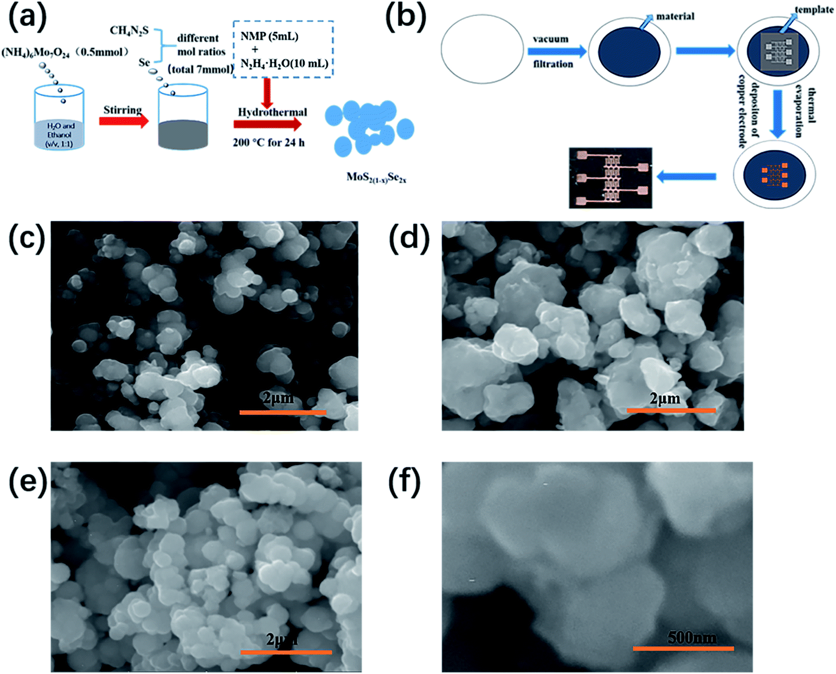 | ||
| Fig. 1 (a) Schematic diagram of MoS2(1−x)Se2x synthesis, (b) schematic diagram of device preparation, and SEM images of (c) MoS2, (d) MoSe2 and (e and f) MoSSe. | ||
XRD measurements have been performed to explore the structural characterization of the as-prepared samples. The XRD pattern of the MoS2 sample showed that the diffraction peaks located at angles (2θ) of about 34.9° and 58.8°, correspond to the (100) and (110) crystal faces of hexagonal MoS2, which is consistent with the literature. For the MoSe2 sample, three broad XRD peaks were observed at 2θ = 33.8°, 41.6° and 54.4°, corresponding to the (100), (103) and (110) crystal planes of the hexagonal MoSe2 (ref. code # 98-060-1045).20–22 Three characteristic peaks at angles of 34.3°, 42.7° and 56.4° can be observed in the XRD pattern of the MoSSe sample. However, compared with the characteristic peaks of MoSe2, the positions are shifted to a certain degree and the intensity of the characteristic peaks is weakened. This is because the radius of the Se atom is larger than that of the S atom, which leads to a change in the lattice distance.23,24 The XRD patterns of all samples showed high noise, which indicates that the crystallinity of the samples was low, and no other peaks were observed, indicating that there were no phase impurities in the samples.
In addition, UV-vis spectra of the MoSSe, MoS2 and MoSe2 are displayed in Fig. 2(b). From the absorption spectrum comparison of the three samples, it can be known that the absorption capacity of the spectrum absorption intensity in the range of 400 nm to 800 nm is MoSe2 > MoSSe > MoS2, which is consistent with the literature.25–27 The UV-vis spectra show that the absorption edges of MoSSe, MoS2 and MoSe2 are about 826 nm, 760 nm, 864 nm, respectively. According to the formula:28 , where E, h, λ and c are the band gap energy of the semiconductor material, Planck constant, wavelength of light and speed of light, respectively. Therefore, the band gaps of MoSSe, MoS2 and MoSe2 can be calculated to be approximately 1.5 eV, 1.63 eV and 1.43 eV, respectively, which is the same as the previous report.29
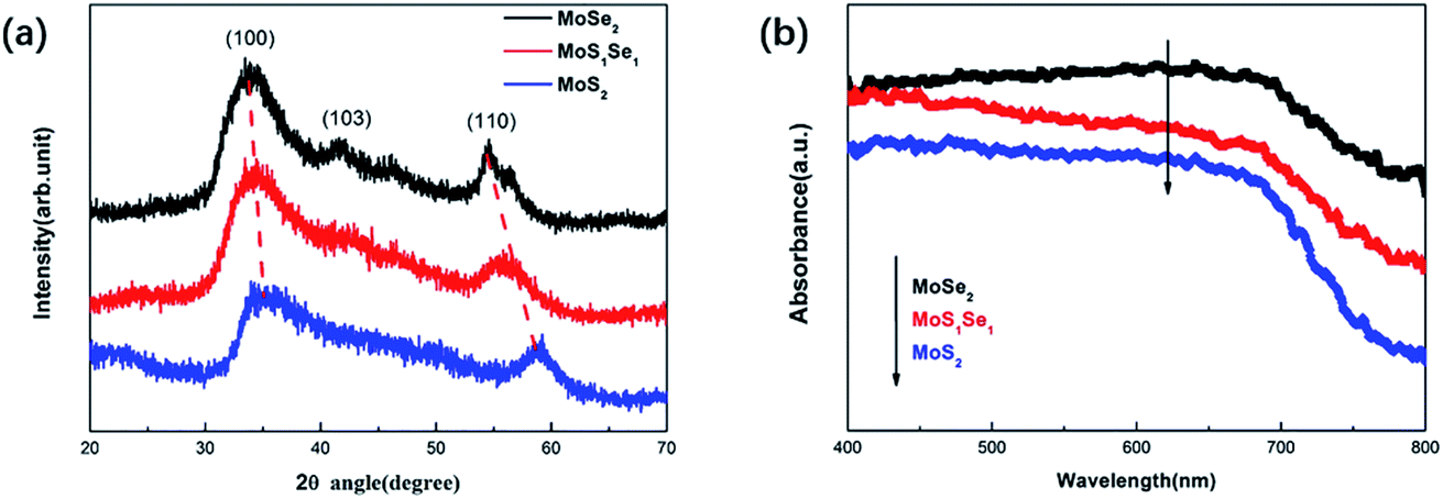 | ||
| Fig. 2 (a) XRD patterns of MoS2, MoSSe and MoSe2, and (b) UV-vis spectra of MoS2, MoSSe and MoSe2. | ||
Fig. 3(a) shows the current–voltage (I–V) characteristics of the MoSSe sample. By comparing dark conditions at a constant power density (1.75 mW mm−2) and laser irradiation at different wavelengths, it was found that the maximum photocurrent response can be obtained under 660 nm irradiation. The linearity of the current–voltage curve can be attributed to the ohmic contact between the sample and the metal electrode,30 which is considered to be beneficial for the extraction of photo-generated carriers. To further explore the sensitivity of photodetectors at different wavelengths, Fig. 3(b) shows the photoresponse over time at a low voltage and the same power density. The photocurrent under laser irradiation of 405 nm, 450 nm, 532 nm, 660 nm and 808 nm is 12.3 μA, 9.3 μA, 8.7 μA, 12.6 μA, and 8.0 μA, respectively. At the same time, it can be seen that these devices show stable and repeatable photoresponse characteristics under irradiation with five lasers of different wavelengths. Fig. 3(c) shows the photoresponse of MoSSe samples over time at a constant power density and different bias voltages. As the voltage increases, the dark current and photocurrent also increase. This is a reflection of the potential gradient caused by the external bias in MoSSe. By controlling the external bias, the photocurrent can be reasonably optimized. Response time (rise time and fall time) is an important parameter of light detection. Rise time (tr) is defined as the time taken for the photogenerated current to rise from 10% to 90% and the time required to reduce the photogenerated current from 90% to 10% is defined as the fall time (tf).31 The rise and fall times of MoSSe photodetectors at a constant power density of 1.75 mW mm−2 and 1 V are 4.7 s and 4.7 s, as shown in Fig. 3(d). Compared with other photodetectors, the performance of our prepared devices is not very outstanding. This is because (1) the crystallinity of the material synthesized by the hydrothermal method is low; (2) the materials are stacked together, causing the photo-generated carriers to be scattered by impurities and defects; (3) the distance between the source and drain of the device is too long, which results in a longer carrier transmission path.
 | ||
| Fig. 3 Photoelectric characteristics of the MoSSe photodetector (a) I–V curves at different wavelengths under dark conditions and at constant power (1.75 mW mm−2), (b) the time-dependent photoresponse under irradiation with various lasers of 1.75 mW mm−2 at 1 V bias, (c) time-dependent photoresponse at different voltages, and (d) rise and fall times at a 1 V potential. | ||
Fig. 4(a) and (b) show the I–V and time-dependent photoresponse under 660 nm laser irradiation at different optical power densities, respectively. The results show that the photocurrent increases with increasing light intensity. This is because a higher light intensity generates more non-equilibrium carriers, which leads to an increase in photocurrent. Meanwhile, the steady photocurrent is about 3.56 μA when the light intensity is 0.75 mW mm−2. The value of responsivity (R) can be obtained from the following equation:32,33R = I/Jlight, where I is the photocurrent density and Jlight is the irradiance intensity. The relationship between photoelectric responsivity and irradiance power intensity is shown in Fig. 4(c). The optical responsivity of the device can reach 1.753 mA W−1. In addition to photoelectric responsivity, the stability of photodetectors is another key factor that should be evaluated before practical application. Hence, cycling stability measurements were performed on the device and are shown in Fig. 4(d). Through continuous switching operation of the device for 900 s, it is found that the photocurrent has almost no attenuation, which indicates that the stability of the device is relatively high, and it also shows that the MoSSe alloy synthesized using the hydrothermal method has high stability. It can also be found that the dark current increases with time. This is because the trapped state in the channel material would prolong the life of the non-equilibrium carriers so the dark current would take longer to recover to the initial equilibrium state.
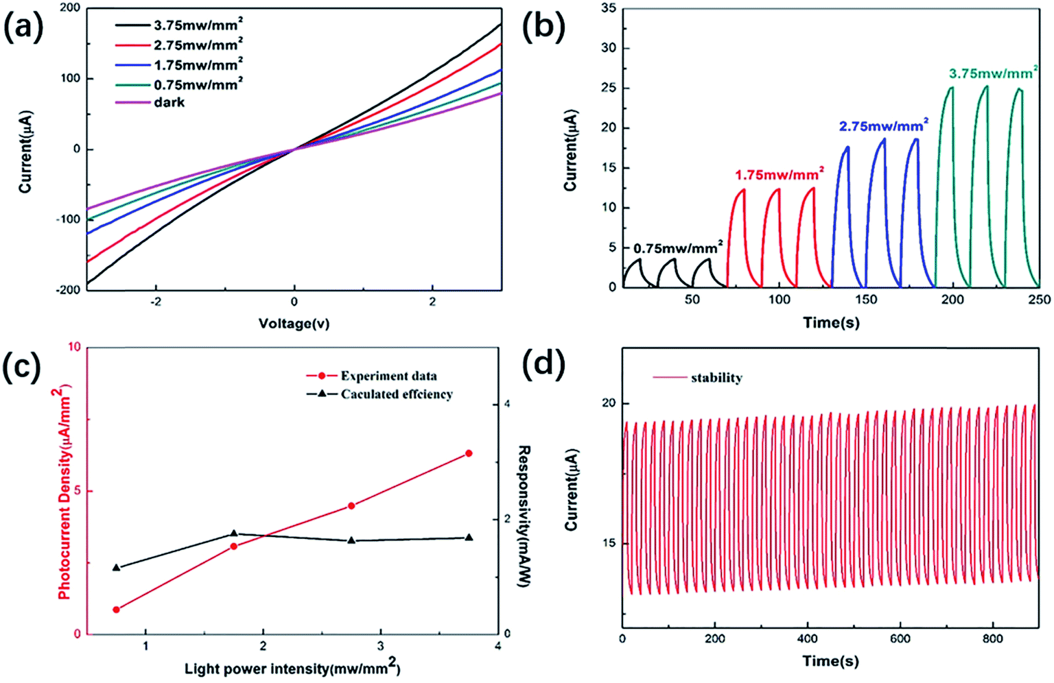 | ||
| Fig. 4 (a) The I–V curves of MoSSe samples under dark conditions and at different power densities, (b) photocurrent of the device at various power densities, (c) calculated photoconversion efficiencies of the device at various power densities, and (d) cycling stability measurements of the device. | ||
Fig. 5(a)–(c) show the time-dependent photoresponse of the three samples MoS2, MoSSe and MoSe2 at a constant power and different bias voltages. As a result, the photocurrent of the MoSSe-based device was higher than that of the MoS2 and MoSe2-based devices, as expected. This is because binary TMD will generate defects of S group vacancies during high temperature synthesis, and these defects will cause DLDSs. On the one hand, DLDSs act as scattering centers, which impede carrier transmission. At the same time, DLDSs are effective recombination centers of photo-generated electron–hole pairs, which greatly shorten the carrier lifetime.34Fig. 5(d) shows the schematic plot of the concept for suppressing DLDSs in MoSSe compared to MoS2 and MoSe2 by alloy engineering. As shown in Fig. 5(d), the energy state of the conduction band minimum of MoSSe is lower than the energy state of MoS2 and is close to the energy state of MoSe2. Therefore, the S vacancy in MoSSe can transfer the captured electrons back to the conduction band to become free electrons, instead of combining with holes in the valence band.11 This will help reduce the recombination of photogenerated electron–hole pairs and increase the lifetime of photogenerated carriers.
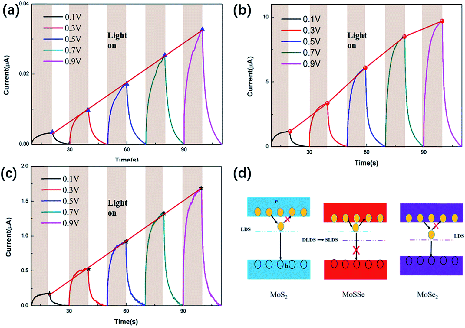 | ||
| Fig. 5 The photocurrents of (a) MoS2, (b) MoSSe and (c) MoSe2 at different bias voltages, and (d) schematic plot of the concept for suppressing DLDSs in MoSSe compared to MoS2 and MoSe2 by alloy engineering. | ||
4. Conclusions
In summary, we synthesized MoS2(1−x)Se2x (x = 0, 0.5, 1) nanostructures via a simple hydrothermal method. The filter membrane was directly used as a substrate by vacuum filtration, and the copper electrode was thermally evaporated and deposited on the surface of the material. The experimental results show that the photodetector based on the alloyed MoSSe material has a higher photocurrent at the same bias voltage and constant power, and the photodetector shows a stable and repeatable photoresponse at different wavelengths of incident light. At the same time, we have compared with some related photodetectors (Table 1), and we can see that our photodetectors have some advantages in terms of response time. All the results show that this work provides a feasible method for the development of low-cost, wide-spectrum (visible spectral range) photodetectors.| Device structure | Method | Wavelength (nm) | Responsivity (mA W−1) | τ r/τf (s) | Ref. |
|---|---|---|---|---|---|
| a Photoconductive type. b Phototransistors. | |||||
| Ti/MoS2/Si/Aub | Thermal decomposition | 550 | — | 13/30 | 35 |
| Au/MoS2/Aua | Mechanical exfoliation | 561 | 8.8 × 10⁵ | 4/9 | 36 |
| MoSe2/Sib | CVD | 650 | 0.26 | 0.025/0.025 | 37 |
| Ti/MoSe2/Tib | Mechanical exfoliation | 532 | 9.7 × 10⁴ | 0.015/0.030 | 38 |
| Ti/Mo0.5W0.5Se2/Aua | PLD | 532 | 77.1 × 10³ | — | 10 |
| Au/MoS1.15Se0.85/Aua | CVD | 532 | 2.06 × 10³ | 18/35 | 39 |
| Cu/MoSSe/Cua | Hydrothermal | 660 | 1.753 | 4.7/4.7 | This work |
Conflicts of interest
There are no conflicts of interest to declare.Acknowledgements
This work was supported by the Grants from the Provincial Natural Science Foundation of Hunan (No. 2019JJ50612), the Open Fund based on innovation platform of Hunan Colleges and Universities (No. 18K032), the National Natural Science Foundation of China (No. 11504312 and 51772255), the Scientific Research Fund of the Hunan Provincial Education Department (No. 18A059), the Program for Changjiang Scholars and Innovative Research Team in University (IRT_17R91) and the Science and Technology Program of Xiangtan (No. CXY-ZD20172002).References
- A. C. Neto, F. Guinea, N. M. Peres, K. S. Novoselov and A. K. Geim, Rev. Mod. Phys., 2009, 81, 109 CrossRef.
- J. Nilsson, A. C. Neto, F. Guinea and N. Peres, Phys. Rev. Lett., 2006, 97, 266801 CrossRef PubMed.
- S. J. Wang, Y. Geng, Q. Zheng and J.-K. Kim, Carbon, 2010, 48, 1815–1823 CrossRef CAS.
- C. Xie, C. Mak, X. Tao and F. Yan, Adv. Funct. Mater., 2017, 27, 1603886 CrossRef.
- Z. Li, H. Qiao, Z. Guo, X. Ren, Z. Huang, X. Qi, S. C. Dhanabalan, J. S. Ponraj, D. Zhang and J. Li, Adv. Funct. Mater., 2018, 28, 1705237 CrossRef.
- Q. H. Wang, K. Kalantar-Zadeh, A. Kis, J. N. Coleman and M. S. Strano, Nat. Nanotechnol., 2012, 7, 699 CrossRef CAS PubMed.
- Z. Huang, W. Han, H. Tang, L. Ren, D. S. Chander, X. Qi and H. Zhang, 2D Mater., 2015, 2, 035011 CrossRef.
- Q. Ou, Y. Zhang, Z. Wang, J. A. Yuwono, R. Wang, Z. Dai, W. Li, C. Zheng, Z. Q. Xu and X. Qi, Adv. Mater., 2018, 30, 1705792 CrossRef PubMed.
- M. J. Park, K. Park and H. Ko, Appl. Surf. Sci., 2018, 448, 64–70 CrossRef CAS.
- Z. Zheng, J. Yao and G. Yang, ACS Appl. Mater. Interfaces, 2017, 9, 14920–14928 CrossRef CAS PubMed.
- J. Yao, Z. Zheng and G. Yang, ACS Appl. Mater. Interfaces, 2016, 8, 12915–12924 CrossRef CAS PubMed.
- B. Huang, M. Yoon, B. G. Sumpter, S.-H. Wei and F. Liu, Phys. Rev. Lett., 2015, 115, 126806 CrossRef PubMed.
- J.-G. Song, G. H. Ryu, S. J. Lee, S. Sim, C. W. Lee, T. Choi, H. Jung, Y. Kim, Z. Lee and J.-M. Myoung, Nat. Commun., 2015, 6, 7817 CrossRef PubMed.
- Y. Chen, W. Wen, Y. Zhu, N. Mao, Q. Feng, M. Zhang, H.-P. Hsu, J. Zhang, Y.-S. Huang and L. Xie, Nanotechnology, 2016, 27, 445705 CrossRef PubMed.
- S. Tongay, J. Zhou, C. Ataca, J. Liu, J. S. Kang, T. S. Matthews, L. You, J. Li, J. C. Grossman and J. Wu, Nano Lett., 2013, 13, 2831–2836 CrossRef CAS PubMed.
- K. Gu, S. Yu, K. Eshun, H. Yuan, H. Ye, J. Tang, D. E. Ioannou, C. Xiao, H. Wang and Q. Li, Nanotechnology, 2017, 28, 365202 CrossRef PubMed.
- Y. R. Lim, J. K. Han, Y. Yoon, J. B. Lee, C. Jeon, M. Choi, H. Chang, N. Park, J. H. Kim and Z. Lee, Adv. Mater., 2019, 31, 1901405 CrossRef PubMed.
- H. I. Lee, H. Yu, C. K. Rhee and Y. Sohn, Appl. Surf. Sci., 2019, 489, 976–982 CrossRef CAS.
- W. J. Kim, D. Pradhan, B.-K. Min and Y. Sohn, Appl. Catal., B, 2014, 147, 711–725 CrossRef CAS.
- Q. Jiang, Y. Lu, Z. Huang and J. Hu, Appl. Surf. Sci., 2017, 402, 277–285 CrossRef CAS.
- H. Tang, H. Huang, X. Wang, K. Wu, G. Tang and C. Li, Appl. Surf. Sci., 2016, 379, 296–303 CrossRef CAS.
- J. Yang, C. Wang, H. Ju, Y. Sun, S. Xing, J. Zhu and Q. Yang, Adv. Funct. Mater., 2017, 27, 1703864 CrossRef.
- Z. Lin, B. Lin, Z. Wang, S. Chen, C. Wang, M. Dong, Q. Gao, Q. Shao, T. Ding and H. Liu, ChemCatChem, 2019, 11, 2217–2222 CrossRef CAS.
- R. Bar-Ziv, O. E. Meiron and M. Bar-Sadan, Nanoscale, 2018, 10, 16211–16216 RSC.
- O. Meiron, L. Houben and M. Bar-Sadan, RSC Adv., 2015, 5, 88108–88114 RSC.
- J. Mao, Y. Yu, L. Wang, X. Zhang, Y. Wang, Z. Shao and J. Jie, Adv. Sci., 2016, 3, 1600018 CrossRef PubMed.
- B. Bajorowicz, A. Cybula, M. Winiarski, T. Klimczuk and A. Zaleska, Molecules, 2014, 19, 15339–15360 CrossRef PubMed.
- X. Chen, Z. Huang, X. Ren, G. Xu, J. Zhou, Y. Tao, X. Qi and J. Zhong, ChemNanoMat, 2018, 4, 373–378 CrossRef CAS.
- F. Ersan, G. k. Gökoğlu and E. Aktürk, J. Phys. Chem. C, 2015, 119, 28648–28653 CrossRef CAS.
- J. Li, J. Han, H. Li, X. Fan and K. Huang, Mater. Sci. Semicond. Process., 2020, 107, 104804 CrossRef CAS.
- J. Wu, S. Ding, Z. Huang, H. Li, K. Huang, X. Qi and J. Li, Fullerenes, Nanotubes, Carbon Nanostruct., 2019, 27, 566–571 CrossRef CAS.
- Q. Hong, Y. Cao, J. Xu, H. Lu, J. He and J.-L. Sun, ACS Appl. Mater. Interfaces, 2014, 6, 20887–20894 CrossRef CAS PubMed.
- Z. Xie, C. Xing, W. Huang, T. Fan, Z. Li, J. Zhao, Y. Xiang, Z. Guo, J. Li and Z. Yang, Adv. Funct. Mater., 2018, 28, 1705833 CrossRef.
- H. Shi, R. Yan, S. Bertolazzi, J. Brivio, B. Gao, A. Kis, D. Jena, H. G. Xing and L. Huang, ACS Nano, 2013, 7, 1072–1080 CrossRef CAS PubMed.
- Y. R. Lim, W. Song, J. K. Han, Y. B. Lee, S. J. Kim, S. Myung, S. S. Lee, K. S. An, C. J. Choi and J. Lim, Adv. Mater., 2016, 28, 5025–5030 CrossRef CAS PubMed.
- O. Lopez-Sanchez, D. Lembke, M. Kayci, A. Radenovic and A. Kis, Nat. Nanotechnol., 2013, 8, 497–501 CrossRef CAS PubMed.
- Y.-H. Chang, W. Zhang, Y. Zhu, Y. Han, J. Pu, J.-K. Chang, W.-T. Hsu, J.-K. Huang, C.-L. Hsu and M.-H. Chiu, ACS Nano, 2014, 8, 8582–8590 CrossRef CAS PubMed.
- A. Abderrahmane, P. Ko, T. Thu, S. Ishizawa, T. Takamura and A. Sandhu, Nanotechnology, 2014, 25, 365202 CrossRef CAS PubMed.
- Y. R. Lim, J. K. Han, Y. Yoon, J. B. Lee, C. Jeon, M. Choi, H. Chang, N. Park, J. H. Kim and Z. Lee, Adv. Mater., 2019, 31, 1901405 CrossRef PubMed.
| This journal is © The Royal Society of Chemistry 2020 |