DOI:
10.1039/D0NA00023J
(Paper)
Nanoscale Adv., 2020,
2, 1465-1472
Synthesis and characterization of Ge-core/a-Si-shell nanowires with conformal shell thickness deposited after gold removal for high-mobility p-channel field-effect transistors†
Received
10th January 2020
, Accepted 6th March 2020
First published on 11th March 2020
Abstract
Ge-core/a-Si-shell nanowires were synthesized in three consecutive steps. Nominally undoped crystalline Ge nanowires were first grown using a vapor–liquid–solid growth mechanism, followed by gold catalyst removal in an etching solution and deposition of a thin layer of amorphous silicon on the nanowire surface using a chemical vapor deposition method. Catalyst removal is necessary to avoid catalyst melting during temperature increase prior to a-Si shell deposition. Field effect transistors based on Ge-core/a-Si-shell nanowires exhibited p-channel depletion-mode characteristics as a result of free hole accumulation in the Ge channel. Scaled on-currents and transconductances up to 3.1 mA μm−1 and 4.3 mS μm−1, respectively, as well as on/off ratios and field-effect hole mobilities up to 102 and 664 cm2 V−1 s−1, respectively, were obtained for these Ge-core/a-Si-shell nanowire FETs. The minimum subthreshold slope was measured to be 300 mV dec−1. The present work also demonstrates for the first time the conductance quantization in one-dimensional Ge-core/a-Si-shell nanowires at low temperatures. The quantization of conductances at discrete values of G0 = 2e2/h at low temperatures suggests that our Ge-core/a-Si-shell nanowires are multi-mode ballistic conductors with a mean-free-path up to 500 nm. The results provided here are relevant for the synthesis of high-quality Ge-core/Si-shell nanowires for high-mobility devices with transparent contacts to hole carriers.
Introduction
Semiconductor nanowires are promising for future applications in nanoscale electronics, photonics, and life sciences.1 Germanium is re-emerging as one of the alternative channel materials for field-effect transistor (FET) applications because it has a higher carrier mobility than that of silicon2 and a higher hole mobility than that of compound semiconductors of group III–V elements.3 Silicon and germanium belong to group IV of the periodic table of elements because they possess similar chemical and physical properties. Therefore, we can expect it to be easier to integrate Ge with Si in current semiconductor technology. However, unlike Si, Ge does not form a stable native oxide. The oxide layer which forms on the Ge surface upon exposure to air is susceptible to surface degradation during exposure to water vapor contained in air. Surface passivation of Ge nanowires has been demonstrated using organic layers, e.g. alkanethiols4 and aqueous halide solutions,5 and dielectric layers, e.g. aluminium oxide (Al2O3) and hafnium oxide (HfO2).6 In the early 2000s, Lauhon et al. demonstrated for the first time the synthesis of Ge-core/Si-shell nanowire heterostructures.7 A thin amorphous Si shell is deposited in situ following Ge nanowire growth. The amorphous Si shell is completely crystallized after thermal annealing at 600 °C. The Si shell not only serves as a passivation layer but also creates a quantum well of holes at the heterostructure interface because of the valence band offset between Ge and Si.8 The devices fabricated from Ge-core/Si-shell nanowires exhibit p-channel depletion-mode (normally on) FET characteristics with hole mobilities up to 730 cm2 V−1 s−1 in the linear region (drain voltage |Vd| = 10 mV).9 However, we observed that in situ deposition of Si shells after Ge nanowire growth was typically accompanied by spreading of gold (Au) nanoparticles on the Ge nanowire sidewalls because of the disparity in temperatures for Ge core growth and Si shell deposition. As a result, when disilane (Si2H6) as the silicon source was introduced, very narrow Si nanowires grew along the Ge nanowire surface (Au nanoparticles on the Ge nanowire sidewalls served as catalysts for Si nanowire growth).10 Goldthorpe et al. removed the gold from the tip of the nanowires ex situ prior to growing Si shells.11 However, the Si shells developed a surface with periodic roughness and likely triggered the nucleation of misfit dislocation at the Ge-core/Si-shell interface. This may affect the electrical transport properties of Ge-core/Si-shell nanowires. In this work, we report studies on the surface passivation of Ge nanowires using amorphous Si (a-Si) shells deposited by the chemical vapor deposition (CVD) method. The deposition parameters of Si shells were optimized to obtain a uniform layer of a-Si with a controlled thickness. The electrical transport properties of the devices fabricated from Ge-core/a-Si-shell nanowires were examined at room temperature and low temperatures. The devices exhibit p-channel field-effect transistor characteristics with high mobilities. Conductance quantization was observed at low temperatures.
Experimental procedure
Nominally undoped Ge nanowires were first prepared using a method reported previously.12 No dopant gases were intentionally flowed during Ge nanowire growth. One may suggest that the removal of the gold catalyst by means of etching will introduce gold impurities into the nanowires thus affecting the transport in the nanowire. However, we have shown in our previous work that this etching actually helps to ensure that the transport in the Ge core is not due to the gold impurities.12 Thus, we can conclude that the Ge nanowires are nominally undoped. These Ge nanowires were then treated in a 10% HCl solution to remove any native oxides from their surface followed by a-Si deposition in a low-pressure chemical vapor deposition chamber. To deposit a-Si, the temperature was ramped up from room temperature to 450 °C (deposition temperature). After a constant temperature was reached, Si2H6 diluted in H2 was introduced into the chamber. The partial pressure and flow rate of Si2H6 were kept constant at 0.3 Torr and 0.5 sccm, respectively, during deposition. The thickness of amorphous silicon was controlled by tuning the deposition time. The Ge-core/a-Si-shell nanowires were characterized using a JEM-2010F field-emission transmission electron microscope (FE-TEM) coupled with an energy-dispersive X-ray spectrometer (EDS).
To fabricate nanowire FETs, substrates that contain Ge-core/a-Si-shell nanowires were suspended in isopropanol and ultrasonically agitated to remove the nanowires from the growth substrate. The nanowires were then drop-cast onto pre-patterned substrates (100 thermally grown SiO2/Si substrates). Electrical contacts to the nanowires were made by defining source and drain electrodes separated by 400–1200 nm with JEOL-JBX5FE electron-beam lithography, evaporation of 100 nm-thick Ni, and subsequent lift-off in acetone. Before Ni evaporation, the sample was dipped in buffered hydrofluoric acid for 3 s to remove any native oxides from the nanowire surface. 5 nm-thick hafnium oxide (HfO2) (dielectric constant = 24) was then deposited on the devices using the atomic layer deposition process. Finally, the top-gate electrode was defined by electron-beam lithography, followed by evaporation of Ni/Au (5 nm/50 nm) and lift-off in acetone. The top-gate electrode forms an omega-shaped gate that is partly wrapped around the nanowire. The electrical transport properties of the devices at room temperature and low temperatures were measured using a probe station (Cascade Microtech) and a physical property measurement system (PPMS, Quantum Design), respectively.
Results and discussion
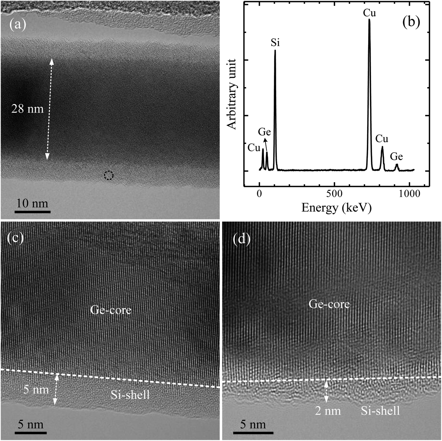
Fig. 1(a) shows a transmission electron microscope (TEM) image of a Ge-core/a-Si-shell nanowire. The elemental composition of the shell was examined by EDS analysis and the corresponding spectrum is given in Fig. 1(b). The Si peak in the EDS spectrum confirms that a-Si was successfully deposited on the Ge nanowire surface. We observe that the thickness of a-Si can be easily controlled by the deposition time. The a-Si thicknesses are 5 and 2 nm for deposition times of 15 and 7 minutes, respectively (Fig. 1(c) and (d)).
 |
| | Fig. 1 (a) TEM image of a Ge-core/a-Si shell nanowire. (b) EDS spectrum of a Si shell at the location denoted by a small circle in (a) showing a strong peak corresponding to Si. The Cu peaks correspond to the TEM grid. (c and d) High-resolution TEM images of a 〈111〉-oriented Ge core with a single-crystalline structure and amorphous Si shell with thicknesses of 5 and 2 nm deposited for 15 and 7 minutes, respectively. | |
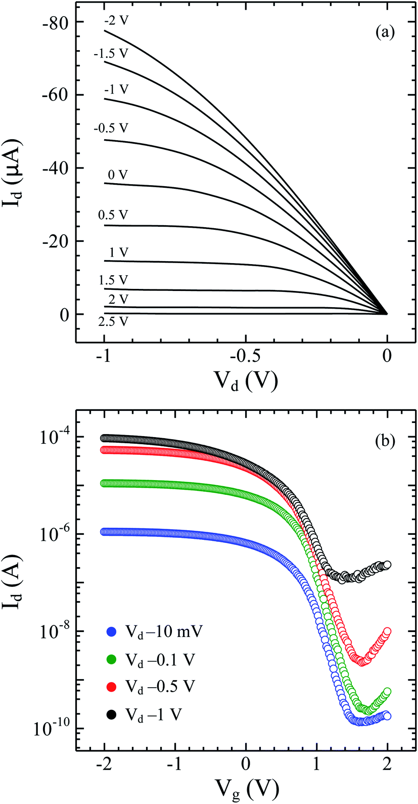
Fig. 2(a) and (b) show typical output (Idversus Vd) and transfer characteristics (Idversus Vg), respectively, at room temperature of top-gated FETs fabricated from a single Ge-core/a-Si-shell nanowire with a channel length of 800 nm. A well-defined transition from a linear to a nearly constant Id with an increasing |Vd| can be seen in the Idversus Vd family of curves. The transfer characteristics show that the drain current Id increases as the gate voltage Vg decreases from +2 to −2 V, and therefore the device is a p-channel depletion-mode FET.2 The ambipolar behavior of all devices measured in the present work is due to the similar transfer characteristics. The devices fabricated from Ge-core/crystalline Si-shell have also been observed to exhibit the p-channel depletion-mode (normally on) FET because the Fermi level lies below the Ge valence band edge in the absence of a gate.9 This result is distinct from that in our previous report on the devices fabricated from undoped Ge nanowires that show characteristics of a p-channel enhancement-mode FET (normally off).12 In the present study, the a-Si layer that coats the Ge nanowire surface causes the Fermi level to be pinned below the Ge valence band edge. As a result, the free holes will accumulate in the Ge channel at zero gate voltage. The valence band offset in the Ge-core/a-Si-shell structure was calculated to be ∼0.87 eV, which is larger than that in the Ge-core/crystalline Si-shell structure (∼0.51 eV) (see Fig. S1 in the ESI†). Amorphous Si is known to have a high defect density due to its disordered structure. The surface states of a-Si contribute significantly to the Fermi level pinning at the Ge-core/a-Si interface. A larger valence band offset and more pronounced Fermi level pinning create a deeper quantum well of holes at the Ge-core/a-Si-shell interface. We also mentioned above that the transfer characteristics show ambipolar behavior. At large positive gate voltages, the Id currents are observed to increase from Vg +1.4 to +2 V due to electron conduction.13 One may believe that the ambipolar behavior is linked to the gold catalyst etching process that introduces nominal impurities into the Ge nanowires. However, we argue that the ambipolar behavior is due to the sole effect of gate voltage application. In the on-state, electron conduction does not occur in the channel because the electrons are located at the conduction band and the Fermi level is way below the valence band of the Ge-core/a-Si-shell system; however at large positive Vg in the symmetrical gate configuration in our device, the electron carriers could be injected via tunneling from the drain due to large conduction band bending. This injection of electrons or minority carriers is indeed a disadvantage during the operation of FETs and can be fully resolved by using asymmetric gate configuration.9 More investigations are needed to know the nature of this minority carrier, such as lifetime and diffusion lengths.
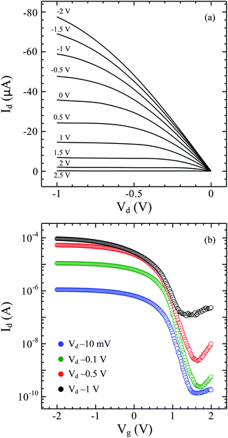 |
| | Fig. 2 (a). Output characteristics (Idversus Vd curve) of the device fabricated from the Ge-core/a-Si shell nanowire with Vg = 2 to −2.5 V in steps of 0.5 V from the top to the bottom. (b) Transfer characteristics (Idversus Vg curve) of the device at Vd = −0.01, −0.1, −0.5 and −1 V. The gate voltage (Vg) was swept from −2 to 2 V. The channel length is 800 nm. | |
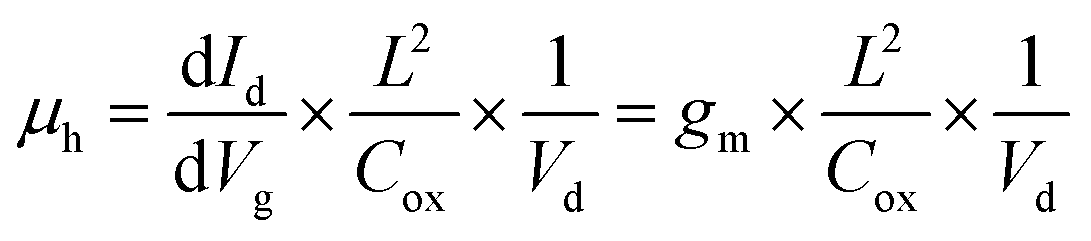
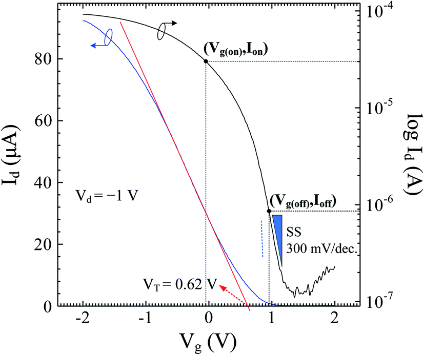
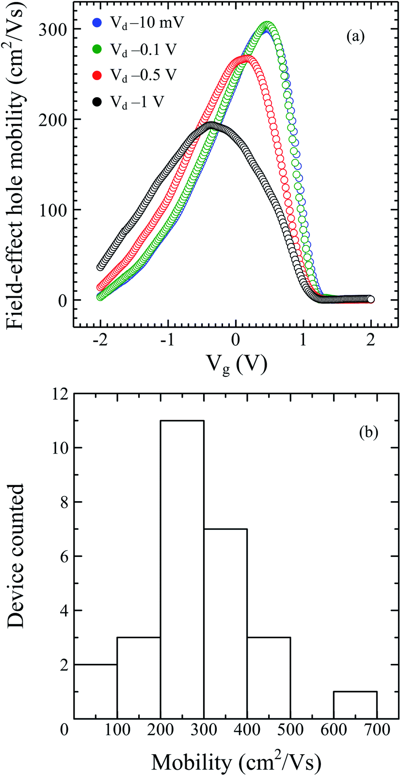
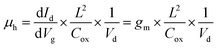
The Idversus Vg transfer characteristics recorded for Vd = −1 V reveal that the Ge-core/a-Si-shell nanowire FET has a maximum transconductance of 46.6 μS and subthreshold slope (SS) of 300 mV dec−1. To obtain the on and off current (Ion and Ioff), the values at Vg(on) = VT − (2/3)Vdd and Vg(off) = VT + (1/3)Vdd were first calculated using the metrics defined in ref. 14, where VT is the threshold voltage and is determined from the intersection of the tangent to the maximum slope and the x-axis of the Id–Vg curve and Vdd is the supply voltage, equal to Vd = 1 V in this case. VT, Vg(on), and Vg(off) were calculated to be 0.62, −0.047, and 0.953 V, respectively (Fig. 3). The values of VT > 0 and Vg(off) > VT are consistent with the characteristics of a p-channel depletion mode FET. From the Id–Vg curve in Fig. 3, the on current is 30.2 μA with a maximum drain current of 92.2 μA. The off current is 0.87 μA with a minimum drain current of 0.12 μA. The on/off ratio is ∼35 calculated from the on and off current. We also estimated the field-effect hole mobility (μh) of this device at different bias voltages using the analytical expression15
| |  | (1) |
where
gm is the transconductance,
L is the channel length underneath the gate electrode, and
Cox is the gate capacitance, and the values are obtained by simulating the Ge-core/a-Si-shell nanowire FET with an omega-shaped gate using COMSOL Multiphysics.
16Fig. 4(a) shows the extracted
μh as a function of
Vg at
Vd = −0.01, −0.1, −0.5, and −1 V. From the
Idversus Vd curve in
Fig. 2(a),
Vd = −0.01 to −0.1 V lie in the linear region whereas
Vd = −0.5 to −1 V lie in the saturation region. In the linear region (lower bias voltages), the field-effect hole mobility
versus Vg curves have a very similar shape with a peak mobility of 304 cm
2 V
−1 s
−1. The peak mobilities at
Vd = −0.5 and −1 V are 267 and 193 cm
2 V
−1 s
−1, respectively (
Fig. 4(a)). The field-effect hole mobility in the saturation region tends to decline because of the increased scattering effects at higher bias voltages. For the 38 Ge-core/a-Si shell nanowire FETs measured in this study, the total yield was 71%, with an average peak mobility of 290 cm
2 V
−1 s
−1 and a highest peak mobility of 664 cm
2 V
−1 s
−1 measured at |
Vd| = 0.1 V (
Fig. 4(b)).
 |
| | Fig. 3 Transfer characteristics for Vd = −1 V on the linear scale (blue curve) and logarithmic scale (black curve). The red line is the tangent to the maximum slope on the linear scale where the intersection of this line and the x-axis denotes the threshold voltage. The on-off currents were calculated using the metrics defined in ref. 14. The subthreshold slope (SS) is 300 mV per decade. The dashed blue line indicates the physical limit of SS (60 mV per decade at room temperature). | |
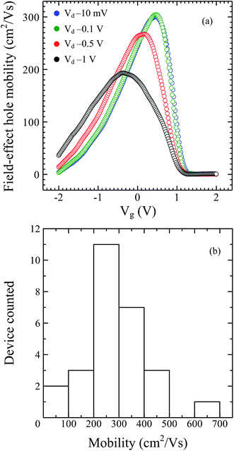 |
| | Fig. 4 (a) Field-effect hole mobility versus gate voltage (Vg) at Vd = −0.01, −0.1, −0.5 and −1 V. (b) Histogram of Ge-core/a-Si shell nanowire FET mobility. | |
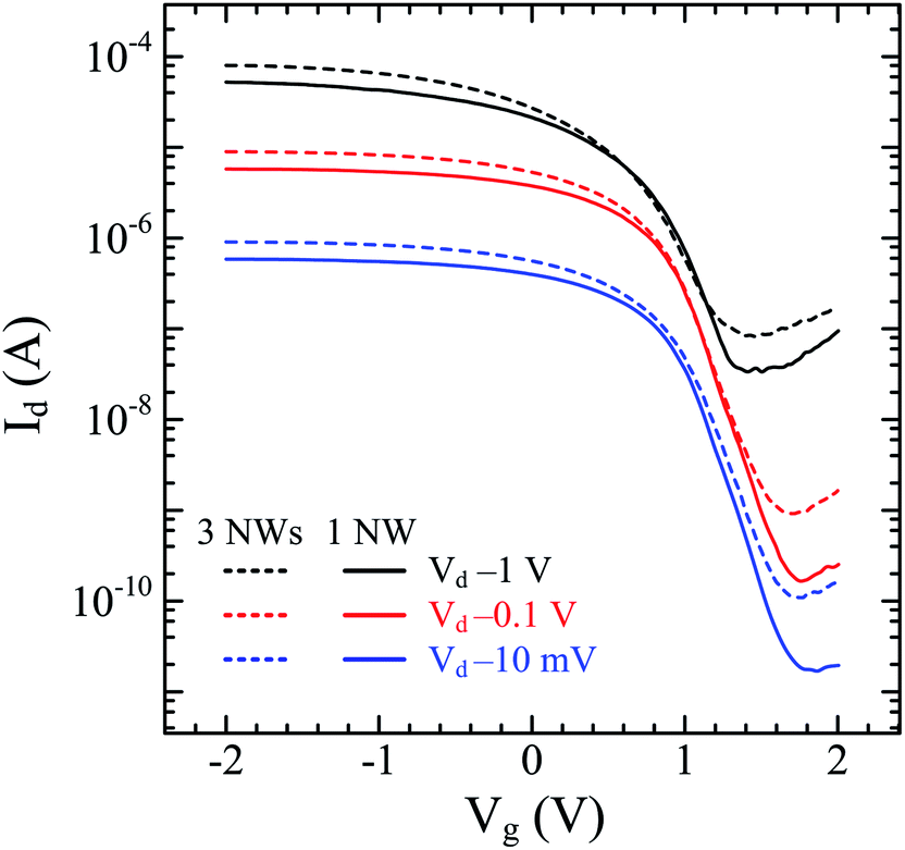
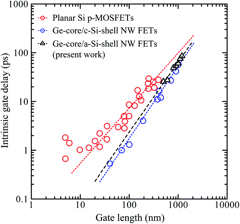
To study the effect of the number of nanowires in our device, we fabricated top-gated FETs consisting of a single nanowire and three nanowires with the same channel length (1 μm). This length is chosen for comparison with the 800 nm channel length device discussed above. The Idversus Vg characteristics of these devices are given in Fig. 5. For the device with a single nanowire, the calculated gm, Ion, Ioff, and on/off ratio are 27.1 μS, 17.3 μA, 0.17 μA, and 100, respectively, and for the device with three nanowires, the calculated gm, Ion, Ioff, and on/off ratio are 44.1 μS, 28.3 μA, 0.71 μA, and 40, respectively. These results show that the devices with shorter channel lengths or multiple nanowire channels exhibit improved gm and Ion but the on/off ratio is compromised. The on current is an important parameter to determine the intrinsic device speed or gate delay (τ), which represents the frequency limit of transistor operation. The intrinsic device speed is calculated using the relationship τ = CoxVdd/Ion.13Fig. 6 shows the intrinsic device speed of seven representative FETs fabricated from a single Ge-core/a-Si nanowire in this work versus the gate length for gate lengths of 500–1200 nm. Planar Si p-MOSFETs14 and Ge-core/crystalline Si-shell nanowire FETs17 are also shown for comparison. The Ge-core/a-Si and Ge-core/crystalline Si-shell nanowire FETs have a quite similar intrinsic device speed although the latter exhibits a steeper slope. Further research is needed to study the intrinsic device speed of the Ge-core/a-Si nanowire FETs as the gate length is further scaled down. Both device types, however, exhibit a much steeper slope (faster intrinsic device speed) than planar Si p-MOSFETs.
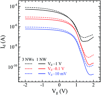 |
| | Fig. 5 Transfer characteristics (Idversus Vg curve) of the devices consisting of a single nanowire (solid curves) and three nanowires (dashed curves) at a Vd of −0.01 V, −0.1 V and −1 V. The gate voltage (Vg) was swept from −2 to 2 V. The channel length is 1 μm. | |
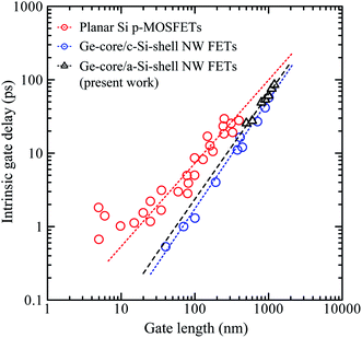 |
| | Fig. 6 Intrinsic device speed or gate delay of Ge-core/a-Si shell nanowire FETs versus gate length. Planar Si p-MOSFETs from ref. 14 and Ge-core/crystalline Si-shell nanowire FETs from ref. 17 are included for comparison. | |
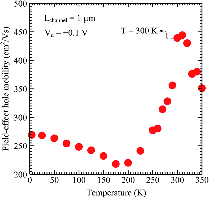
We also carried out temperature-dependent electrical transport measurements to further characterize the Ge-core/a-Si-shell nanowire. To examine the temperature dependence of the field-effect mobility, Vg was first swept from −2 to 2 V (|Vd| was kept constant at 0.1 V). The transconductance was then derived using eqn (1) and the field-effect hole mobility value was selected at a Vg of 0.88 V for each temperature condition (the field-effect mobility at room temperature reaches its peak value at a Vg of 0.88 V). Fig. 7 shows the relationship between the field-effect hole mobility measured at |Vd| = 0.1 V and temperature for a 1 μm channel length device fabricated from a single nanowire. The temperature range in Fig. 7 can be divided into three regions: I (4.2 to 175 K), II (175 to 310 K), and III (310 to 350 K). Region III will be discussed first. In region III, as temperature further increases from 310 to 350 K, the peak mobility decreases due to increased hole-phonon scattering. In region II, as temperature increases from 175 to 310 K, sufficient thermal energy is available to accelerate the hole velocity (the peak mobility increases and reaches its highest value at 310 K) overcoming the surface state scattering. In region I, the peak mobility decreases as temperature increases and reaches its lowest value at 175 K. This can be explained by the dependency of the surface state scattering rate at the boundary between Ge-core/Si-shell on temperature. The surface state is dependent on temperature; as the temperature increases from 4.2 K to 175 K, the ionization of the surface state will increase and the hole carrier will occupy higher radial sub-bands resulting in more hole fractions near the boundary. This increases the scattering rate between hole carriers and the surface state leading to decreasing mobility.18 The temperature-dependent mobility in one-dimensional Ge-core/a-Si-shell systems is distinct from that in two-dimensional hole gas (2DHG) mobility systems studied using planar heterostructures where the mobility decreases monotonically with increasing temperatures due to increased phonon scattering,19–22 whereas in 1D heterostructure systems, the surface state plays an important role at low temperature due to the surface to volume ratio being greatly enhanced compared to that of 2D systems. To the best of our knowledge, temperature-dependent mobility in one-dimensional Ge-core/a-Si-shell has never been reported before. Our result demonstrates a unique feature of one-dimensional hole gas.
 |
| | Fig. 7 Field-effect hole mobility versus temperature calculated at Vd = −0.1 V. The field-effect hole mobility value was selected at Vg 0.88 V for each temperature condition. | |
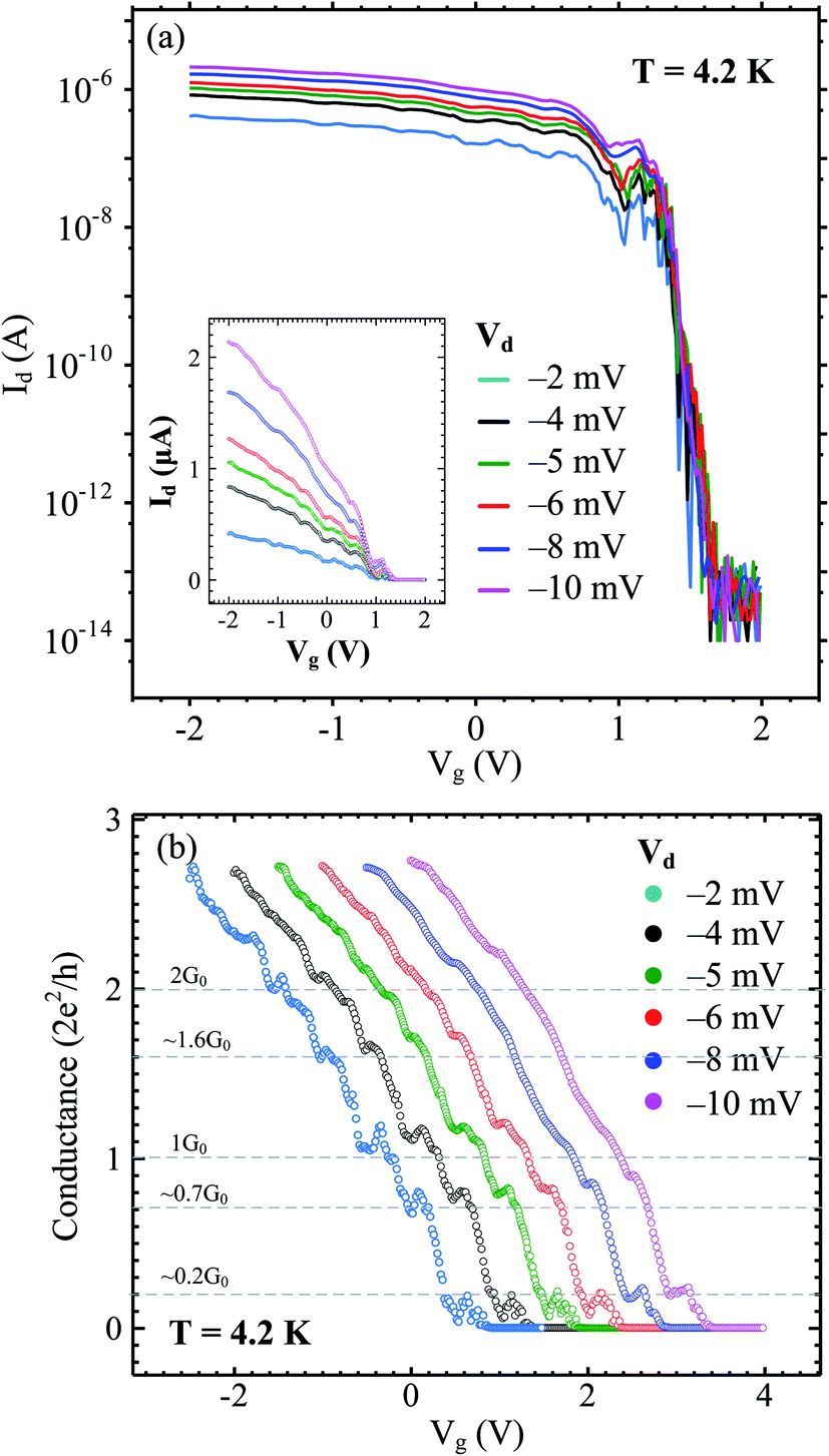
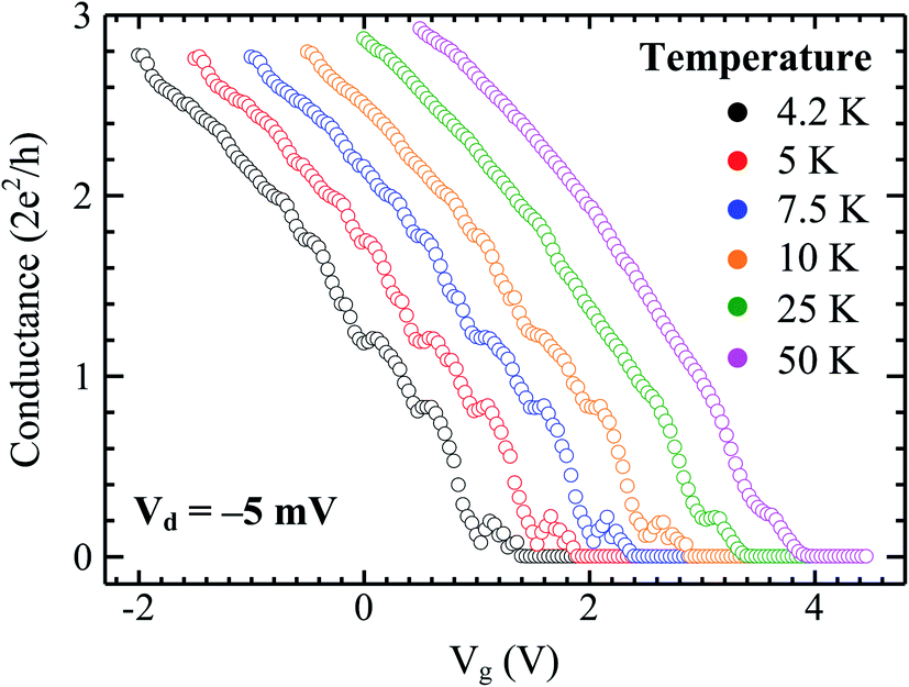
We also fabricated a 500 nm channel length device and studied its temperature-dependent electrical transport. The low-field transfer characteristics of this device with various bias voltages (Vd = −2, −4, −5, −6, −8, and −10 mV) at 4.2 K are shown in Fig. 8(a). Current oscillations are observed at each given Vd, probably corresponding to the quantum transport behaviors of holes in confined one-dimensional structures. To further explore this phenomenon, we calculated the conductance by dividing the measured drain currents by the applied drain voltages and plotted it against the gate voltages in units of G0 (Fig. 8(b)). The stepwise features are observed in each conductance plot and they correspond to the quantization of the channel density of states. The stepwise features become negligible at Vd = −10 mV which can be attributed to carrier-heating effects.
 |
| | Fig. 8 (a) Transfer characteristics on the logarithmic scale of the devices fabricated from the Ge-core/a-Si shell nanowire with a channel length of 500 nm at low Vd (−2, −4, −5, −6, −8 and −10 mV) at T = 4.2 K. Inset: transfer characteristics on the linear scale. (b) Extracted conductances from (a) showing stepwise features at several G0 values including the quantization at ∼0.7G0 (“0.7 structure”). The x-axis has been shifted to the right for clarity of comparison. | |
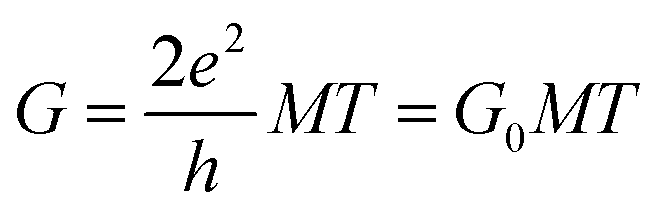
The mean free path of Ge-core/crystalline Si-shell is calculated to be 540 nm.8 Ballistic conduction is expected to be observable when the channel length is comparable to or shorter than the mean free path. Low-temperature measurements are desirable to suppress scattering due to thermal vibrations. We could expect that the transport in our Ge-core/a-Si shell nanowire approaches ballistic conduction at low temperature. Our claim is supported by the conductance values near the zero source-drain voltage that show stepwise features at 1G0 and 2G0 (Fig. 8(b)). This suggests that the mean-free-path in our Ge-core/a-Si nanowires is equivalent to the channel length which is up to 500 nm. These steps agree with the Landauer formula of multi-modes of ballistic conductors23
| |  | (2) |
where
G is the conductance,
G0 is the value of the quantum conductance and is equal to 7.748 × 10
−5 S,
e is the electron charge,
M is the number of transverse modes and
T is the transmission probability. The transmission probability is related to the contact quality between the electrodes and the hole carrier in the Ge-core/a-Si shell nanowire. We also observed steps at ∼0.7
G0 and ∼0.2
G0 which are not integers. The observation of quantization at ∼0.7
G0 agrees with the work carried out by Lu
et al.8 The quantization at ∼0.7
G0, usually called the “0.7 structure”, corresponds to the spin polarization in low-dimensional conductors.
8,24–26 The quantization at ∼0.2
G0 has been shown to originate from the split of the plateau at 0.5
G0 which usually appears at a very small |
Vd| ≪ 1 mV. However, in our case, this 0.5
G0 plateau does not appear because our
Vd is not close enough to 0 V.
25 At higher
Vd > 1 mV, the 0.5
G0 plateau is expected to split and result in two plateaus observed at ∼0.7
G0 and ∼0.2
G0. Therefore, the ∼0.2
G0 plateau can also be ascribed to the spin polarization. We also observed another non-integer quantization at ∼1.6
G0. Odd plateaus at greater than 1
G0 are usually visible in the regime of high
Vd > 1 mV. It seems that the quantization at ∼1.6
G0 is related to a high
Vd in our experiment.
27 Another possibility is that since the device channel length is close to the theoretical mean free path of 540 nm, defects can also introduce non-discrete conductance above 1
G0 in multi-mode ballistic conductors.
28 We observe that the conduction steps appear at discrete values of 1
G0 and 2
G0. If we eliminate the non-integer quantization plateaus caused by spin polarization and defects, our contact is transparent with
T = 1. The conduction step very close to ∼0.7
G0 also shows the transparency of the contacts because this can only be achieved if the contact is transparent to the hole carrier.
8 Therefore, our Ni contacts provide a transparent contact to the hole gas without the need for annealing the devices.
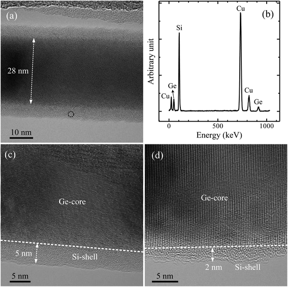
Although we do not measure the plateau of conductance at higher values of G0 due to our data limitation with −2 V ≤ Vg ≤ 2 V (higher values of G0 are useful to determine the maximum transverse mode value), we conclude that our Ge-core/a-Si nanowires are a multi-mode ballistic conductor at low temperatures. This result is distinct from that obtained in the Ge-core/crystalline Si-shell study in which the characteristics of a single-mode ballistic conductor with a maximum conductance plateau at 1G0 are observed.8 In Fig. 8(b), as Vd varies further from 0 V (−2 mV to −6 mV), the plateaus of 1G0 and 2G0 are slightly shifted upward. The effect of the source-drain voltage on the upward shift of the curves was also observed by other researchers in 1-D quantum wires as well as in quantum point contacts (QPCs).24,25,29 The deviation from the discrete value of G0 at high |Vd| is attributed to the sub-band energy separation at the Fermi level approximately close to the value of |Vd|.29 In our experiment, the conductance plateaus at 1G0 and 2G0 start to deviate upward after |Vd| = 2 mV. This suggests that the sub-band energy separation in our Ge-core/a-Si nanowires is between 2 and 4 meV. The finite (non-zero) Vd also contributes to the evolution of the “0.7 structure” approaching a value of ∼0.9G0 at |Vd| = 10 mV.30 The quantization plateaus also become broadened as we increase the temperature from 4.2 K to 50 K (the Vd is kept constant at 5 mV) as shown in Fig. 9. This broadening is also known as thermal smearing. Thermal smearing has been extensively studied theoretically and experimentally in QPCs. The underlying mechanism of this phenomenon is that at high temperatures, the electron states at the lower sub-band are no longer fully occupied because some electrons occupy the electron states in the next sub-band with higher energy. This mechanism leads to energy-averaging of the conductance with an effective energy-averaging parameter ΔE = 4kBT where T is the absolute temperature at which the plateaus almost disappear and kB is the Boltzmann constant.31,32 From Fig. 9, energy-averaging becomes significant above 7.5 K and the stepwise features almost disappear at 10 K. These absolute temperatures correspond to energy-averaging parameters between ∼2.6 meV and ∼3.5 meV, close to the value of the estimated sub-band energy separation mentioned above.
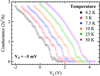 |
| | Fig. 9 Conductance versus gate voltage at Vd = −5 mV measured at various temperatures. The x-axis has been shifted to the right for clarity of comparison. | |
Conclusions
We have demonstrated a facile method for the synthesis of Ge-core/a-Si shell nanowires with precise control over the shell thickness. Field effect transistors with a top gate structure fabricated from Ge-core/a-Si shell exhibit p-channel depletion mode characteristics as a result of the hole confinement in the quantum well formed between the Ge core and Si shell valence band. The devices also exhibit excellent electrical properties such as high transconductance, on-current and field-effect hole mobility. The gate delay or intrinsic device speed of Ge-core/a-Si shell nanowire FETs is expected to be remarkably faster in the short gate-length regime. Conductance quantization is observed at discrete values of G0 at low temperatures showing that the Ge-core/a-Si nanowires are multi-mode ballistic conductors with a mean free path up to 500 nm in our experiment. The “0.7 structure” suggests the occurrence of spin polarization which can be observed if the contacts to the hole carrier are transparent. Finally, the synthesis method presented here can be used to produce high-quality Ge-core/Si-shell nanowires for high-mobility devices. We expect that our method can be applied to synthesize other nanowire heterostructure systems.
Conflicts of interest
There are no conflicts of interest to declare.
Acknowledgements
The authors would like to thank Dr Wei Cao and Professor Kaustav Banerjee of UC Santa Barbara for their help with the coupling capacitance simulation and calculation. This work was supported in part by JSPS KAKENHI Grant Number 26249048.
Notes and references
- Y. Li, F. Qian, J. Xiang and C. M. Lieber, Mater. Today, 2006, 9, 18–27 CrossRef CAS.
-
S. M. Sze, Physics of Semiconductor Devices, Wiley, New York, 1981 Search PubMed.
- R. Pillarisetty, Nature, 2011, 479, 324–328 CrossRef CAS PubMed.
- D. Wang and H. Dai, Appl. Phys. A, 2006, 85, 217–225 CrossRef CAS.
- H. Jagannathan, J. Kim, M. Deal, M. Kelly and Y. Nishi, ECS Trans., 2006, 3, 1175–1180 CAS.
- M. Simanullang, K. Usami, T. Noguchi, A. Surawijaya, T. Kodera, Y. Kawano and S. Oda, Jpn. J. Appl. Phys., 2014, 53, 06JG04 CrossRef.
- L. J. Lauhon, M. S. Gudiksen, D. Wang and C. M. Lieber, Nature, 2002, 420, 57–61 CrossRef CAS PubMed.
- W. Lu, J. Xiang, B. P. Timko, Y. Wu and C. M. Lieber, Proc. Natl. Acad. Sci. U. S. A., 2005, 102, 10046–10051 CrossRef CAS PubMed.
- J. Xiang, W. Lu, Y. Hu, Y. Wu, H. Yan and C. M. Lieber, Nature, 2006, 441, 489–493 CrossRef CAS PubMed.
- When the germane (GeH4) flow was stopped and the temperature was ramped up from the growth temperature of the Ge nanowire to the deposition temperature of a-Si, the catalyst melted, spread from the tip to the surface, and formed gold dots along the surface. When Si2H6 was introduced, these gold dots served as catalysts for Si nanowire growth. See Fig. S2 in the ESI† for a scanning electron microscope (SEM) image of a Ge nanowire covered by narrow Si nanowires.
- I. A. Goldthorpe, A. F. Marshall and P. C. McIntyre, Nano Lett., 2008, 8, 4081–4086 CrossRef CAS PubMed.
- M. Simanullang, G. B. M. Wisna, K. Usami, W. Cao, Y. Kawano, K. Banerjee and S. Oda, J. Mater. Chem. C, 2016, 4, 5102–5108 RSC.
- B. M. Nguyen, Y. Taur, S. T. Picraux and S. A. Dayeh, Nano Lett., 2014, 14(2), 585–591 CrossRef CAS PubMed.
- R. Chau, S. Datta, M. Doczy, B. Doyle, B. Jin, J. Kavalieros, A. Majumdar, M. Metz and M. Radosavljevic, IEEE Trans. Nanotechnol., 2005, 4, 153–158 CrossRef.
- A. C. Ford, J. C. Ho, Y. L. Chueh, Y. C. Tseng, Z. Fan, J. Guo, J. Bokor and A. Javey, Nano Lett., 2009, 9, 360–365 CrossRef CAS PubMed.
- To estimate field-effect hole mobility, the coupling capacitance between the gate electrode and the nanowire was first computed self-consistently using COMSOL Multiphysics®.
- Y. Hu, J. Xiang, G. Liang, H. Yan and C. M. Lieber, Nano Lett., 2008, 8, 925–930 CrossRef CAS PubMed.
- G. W. Holloway, Y. Song, C. M. Haapamaki, R. R. LaPierre and J. Baugh, Appl. Phys. Lett., 2013, 102, 043115 CrossRef.
- Y. H. Xie, D. Monroe, E. A. Fitzgerald, P. J. Silverman, F. A. Thiel and G. P. Watson, Appl. Phys. Lett., 1993, 66, 2263–2264 CrossRef.
- T. Baba, T. Uemura and M. Mizuta, J. Cryst. Growth, 1993, 127, 887–891 CrossRef CAS.
- D. J. Paul, N. Griffin, D. D. Arnone, M. Pepper, C. J. Emeleus, P. J. Phillips and T. E. Whall, Appl. Phys. Lett., 1996, 69, 2704–2706 CrossRef CAS.
- A. Agrawal, M. Barth, H. Madan, Y. Lee, Y. Lin, C. Wu, C. Ko, C. H. Wann, D. Loubychev, A. Liu, J. Fastenau, J. Lindemuth and S. Datta, Appl. Phys. Lett., 2014, 105, 052102 CrossRef.
-
S. Datta, Electronic Transport in Mesoscopic System, Cambridge University Press, Cambridge, 1995 Search PubMed.
- K. J. Thomas, J. T. Nicholls, M. Y. Simmons, M. Pepper, D. R. Mace and D. A. Ritchie, Phys. Rev. Lett., 1996, 77, 135–138 CrossRef CAS PubMed.
- R. Crook, J. Prance, K. J. Thomas, S. J. Chorley, I. Farrer, D. A. Ritchie, M. Pepper and C. G. Smith, Science, 2006, 312, 1359–1362 CrossRef CAS PubMed.
- S. M. Cronenwett, H. J. Lynch, D. Goldhaber-Gordon, L. P. Kouwenhoven, C. M. Marcus, K. Hirose, N. S. Wingreen and V. Umansky, Phys. Rev. Lett., 2002, 88, 226805 CrossRef CAS PubMed.
- N. K. Patel, J. T. Nicholls, L. Martin-Moreno, M. Pepper, J. E. F. Frost, D. A. Ritchie and G. A. C. Jones, Phys. Rev. B: Condens. Matter Mater. Phys., 1991, 44, 13549–13555 CrossRef CAS PubMed.
- S. Frank, P. Poncharal, Z. L. Wang and W. A. de Heer, Science, 2006, 280, 1744–1746 CrossRef PubMed.
- L. P. Kouwenhoven, B. J. van Wees and C. J. P. M. Harmans, Phys. Rev. B: Condens. Matter Mater. Phys., 1989, 39, 8040–8043 CrossRef PubMed.
- A. Kristensen, H. Bruus, A. E. Hansen, J. B. Jensen, P. E. Lindelof, C. J. Markmann, J. Nygard and C. B. Sørensen, Phys. Rev. B: Condens. Matter Mater. Phys., 2000, 62, 10950–10957 CrossRef CAS.
- P. F. Bagwell and T. P. Orlando, Phys. Rev. B: Condens. Matter Mater. Phys., 1989, 40, 1456–1464 CrossRef PubMed.
- B. J. van Wees, L. P. Kouwenhoven, E. M. M. Willems, C. J. P. M. Harmans, J. E. Mooij, H. van Houten, C. W. J. Beenakker, J. G. Williamson and C. T. Foxon, Phys. Rev. B: Condens. Matter Mater. Phys., 1991, 43, 12431–12453 CrossRef PubMed.
Footnote |
| † Electronic supplementary information (ESI) available. See DOI: 10.1039/d0na00023j |
|
| This journal is © The Royal Society of Chemistry 2020 |
Click here to see how this site uses Cookies. View our privacy policy here. 
 Open Access Article
 This Open Access Article is licensed under a Creative Commons Attribution-Non Commercial 3.0 Unported Licence
 *b,
Koichi
Usami
a and
Shunri
Oda
*a
*b,
Koichi
Usami
a and
Shunri
Oda
*a