
 Open Access Article
 This Open Access Article is licensed under a Creative Commons Attribution-Non Commercial 3.0 Unported Licence
In situ fabrication of Al surface plasmon nanoparticles by metal–organic chemical vapor deposition for enhanced performance of AlGaN deep ultraviolet detectors
You
Wu
ab,
Xiaojuan
Sun
 *ab,
Zhiming
Shi
ab,
Yuping
Jia
ab,
Ke
Jiang
ab,
Jianwei
Ben
c,
Cuihong
Kai
ab,
Yong
Wang
ab,
Wei
Lü
ad and
Dabing
Li
*ab
*ab,
Zhiming
Shi
ab,
Yuping
Jia
ab,
Ke
Jiang
ab,
Jianwei
Ben
c,
Cuihong
Kai
ab,
Yong
Wang
ab,
Wei
Lü
ad and
Dabing
Li
*ab
aState Key Laboratory of Luminescence and Applications, Changchun Institute of Optics, Fine Mechanics and Physics, Chinese Academy of Sciences, Changchun 130033, People's Republic of China. E-mail: sunxj@ciomp.ac.cn; lidb@ciomp.ac.cn
bCenter of Materials Science and Optoelectronics Engineering, University of Chinese Academy of Sciences, Beijing 100049, People's Republic of China
cCollege of Materials Science and Engineering, Shenzhen University, Shenzhen 518071, People's Republic of China
dKey Laboratory of Advanced Structural Materials, Ministry of Education, Changchun University of Technology, Changchun 130012, People's Republic of China
First published on 17th March 2020
Abstract
Al nanoparticles (NPs) have been proven to be the efficient choice for plasmon enhanced AlGaN-based ultraviolet (UV) photodetectors. Previous studies have mainly been focused on the ex situ preparation of Al NPs, but the in situ growth of Al NPs is more desired. In this work, we predict the feasibility for in situ growth of Al surface plasmon NPs on AlGaN-based UV photodetectors by first-principles calculations, and realized it experimentally by metal–organic chemical vapor deposition. For metal–semiconductor–metal type AlGaN-based photodetectors with in situ grown Al surface plasmons, the peak of responsivity was at 288 nm, enhanced 9 times more than that without Al NPs at 10 V bias. The in situ growth method of Al NPs in the present work provides an efficient method for improving the performance of AlGaN-based UV photoelectric devices.
Introduction
AlN and AlGaN-based materials are typical representatives of third-generation semiconductor materials with direct transition energy bands and wide band gap, as well as excellent thermal and chemical stability, which are extensively applied to high-performance ultraviolet (UV) and deep-ultraviolet (DUV) photoelectric devices, such as photodetectors (PDs), light emitting diodes (LEDs) and laser diodes (LDs).1–6 Among them, AlGaN-based UV emitters and detectors show potential application in biomedical, sterilization, flame detection and missile warning,7,8 and they have received extensive attention. Different types of AlGaN-based UV photodetectors with promising performance have been demonstrated, such as Schottky type, metal–semiconductor–metal (MSM) type, p–n/p–i–n type and avalanche detectors. However, due to the constraints of material quality and doping difficulties, the device performance is currently far below expectations. Recently, surface plasmon (SP) enhancement by metal nanoparticles (NPs) has provided a new approach to obtain high performance UV optoelectronic devices.Surface plasmon resonance would occur when the frequency of the incident light wave coincides with the oscillation frequency of the electrons. The energy of the electromagnetic field is then effectively converted into the collective vibration energy of the free electrons of metal nanostructures, resulting in an enhanced electromagnetic field. Surface plasmon enhancement has extensive applications in optoelectronic devices,9,10 biological sensors,11,12 and photocatalytic and13 and high resolution imaging.14,15
In theory, the metal nanoparticles surface plasmon effect is related to its quality factor, Qm = −Reεm(ω)/Imεm(ω), where Reεm(ω) and Imεm(ω) is the real and imaginary part of the permittivity.16,17 A larger Qm indicates a stronger plasmon effect in this wavelength. According to their quality factors, Au18,19 and Ag20,21 can be used for visible and near-UV optoelectronic device enhancement, but Al is a good choice to enhance the performance of UV and DUV optoelectronic devices.22–24 In addition, Al SPs have the advantages of low price and a wide range of natural sources. However, the fabrication of Al SPs is difficult due to the high viscosity of the Al material. For Au and Ag NPs, they are easily achieved by rapid thermal annealing after vacuum evaporation. But Al films are usually formed at the beginning instead of Al NPs, when using vacuum evaporation. Even though the Al films are treated by a rapid thermal annealing method, Al NPs cannot be obtained.
Currently major methods for preparing Al NPs as SPs are an ex situ preparation strategy including optimized vacuum evaporation,23 electron beam lithography (EBL),25 nanosphere lithography (NSL),24,26 and nanoimprinting,27 which would cause pollution at the interface between Al NPs and AlGaN, affecting the transfer of energy and carriers from metal plasmons to semiconductor epi-layers. Moreover, Al NPs by ex situ preparation can only be fabricated on the surface of the oriented samples. Since the SP enhancement effect decays exponentially in the direction perpendicular to the interface, it is difficult for ex situ fabricated Al SPs to penetrate the active region and thus limits the applications of the plasmon enhancement effect. To narrow the distance between the NPs and the active layer, M. Razeghi et al.28 used a selective etching process to form holes near the multiple quantum wells (MQWs) and deposited Al in the resulting holes to obtain plasmon enhanced UV-LEDs. However, this method is complicated, time consuming and costly, and will induce additional defects. Therefore, an effective in situ growth method of Al SPs on AlGaN-based materials is highly desired.
In this study, we report a method of in situ growth of Al nanostructures on AlGaN epi-layers by metal–organic chemical vapor deposition (MOCVD), and confirm its excellent plasmon enhancement effect for AlGaN-based MSM type UV PDs. We proposed the novel idea of the in situ growth of Al NPs on AlGaN epi-layers by MOCVD according to the growth kinetics process. Both theoretical calculations and experiments have been studied to confirm the feasibility. Furthermore, the significant enhancement in responsivity for AlGaN-based UV photodetectors with in situ grown Al NPs was verified.
Experimental section
1. Growth details of materials
The 1 μm thick unintentional doping Al0.4Ga0.6N epi-layer was grown on a (0001) sapphire substrate by high-temperature MOCVD at 1180 °C. Before the AlGaN layer was deposited, the substrate was first heated to 1230 °C under a H2 atmosphere to remove surface contamination and then a 1 μm AlN template layer was grown by a two-step growth method. Trimethylgallium (TMGa), trimethylaluminum (TMAl) and ammonia (NH3) were used as Ga, Al and N precursors, respectively. After AlGaN layer growth, all precursors were stopped and only the carrier gas (H2) was used to evacuate the gas chamber. Then, the temperature was decreased to 950 °C, and the Al precursor was separately introduced to fabricate Al NPs. This process is termed as “in situ NP growth” and the schematic diagram of the growth process is illuminated in Fig. 1(a and b). Four samples were grown by varying the growth time of Al (0 s, 15 s, 30 s, and 60 s) and named Sample A, B, C, and D, respectively.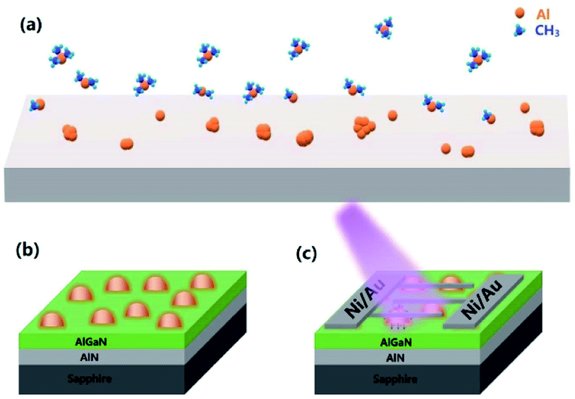 | ||
| Fig. 1 The schematic diagram of the growth process (a), result (b) and device structure (c). | ||
2. Device fabrication
The Ni/Au (50 nm/20 nm) Schottky contacts were fabricated by vacuum evaporation for the interdigitated contacts of the AlGaN MSM type detector and then the samples were treated by rapid thermal annealing at 450 °C for 180 s. The fingers of the interdigitated contacts were 100 μm in length and 10 μm in width with a spacing of 10 μm. These devices were fabricated by standard photolithography and lift-off process. The device structure diagram is shown in Fig. 1(c).3. Characterization
The surface topography of the AlGaN layer with in situ Al NPs was characterized by using the tapping mode of an atomic force microscope (AFM) (Bruker multimode 8). X-ray photoelectron spectroscopy (XPS) measurements were carried out on a spectrometer (VG ESCALAB MKII) with Al Kα X-ray radiation as the excitation source. To study the optical spectral response of the devices, a UV-enhanced Xe arc lamp was used as the light source and a UV-enhanced Si detector was used for calibrating. The incident light was modulated by using a mechanical chopper while the lock-in amplifier was used to record the photocurrent. The current–voltage (I–V) performance of the AlGaN-based detectors was measured by using a Keithley 6487 electrometer.4. First-principles calculations
First-principles calculations were performed by employing the generalized gradient approximation (Perdew–Burke–Ernzerhof parametrization, PBE) and a projector-augmented wave method as implemented in the Vienna Ab initio Simulation Package.29 The vdW interaction30,31 was included in the calculations. A plane-wave basis setting with a kinetic energy of 500 eV was used. We used gamma-only k-points in the calculations. The force and total energy convergence thresholds were set to 0.015 eV Å−1 and 10−5 eV, respectively. Here, a four-layer rectangle Al0.5Ga0.5N supercell containing 240 atoms was used in our calculations. The in-plane lattice parameters of the supercell were larger than 16 Å and the vacuum slabs were thicker than 15 Å to avoid artificial interaction of the periodic images. The N-surface was passivated by hydrogen, and the dangling metal-surface was fully optimized.Results and discussion
According to previous reports on the kinetics of AlGaN-based material growth by MOCVD,32 the metal organic source is decomposed by the heated substrate in a reaction chamber. The decomposition reaction of TMAl could be expressed as follows:| TMAl—Al* + 3CH3 | (1) |
| TMAl—MMAl + 2CH3 | (2) |
| MMAl—Al* + CH3 | (3) |
To demonstrate the clustering behavior of Al atoms on the AlGaN surface, we calculated the total energy of Al atoms adsorbed one by one on the Al0.5Ga0.5N surface. The Al atom adsorption was an exothermic process indicating the stability of the structures. In Fig. 2, we find that the single Al atom preferred binding on the top of N atoms due to the Coulomb interaction. Next, we put one more Al atom close or far from the first one to form an Al dimer or isolated Al atoms respectively. The dimer adsorbed structure exhibited lower energy by 0.65 eV than that of the isolated adsorbed structure. When we further added the third Al atom, the additional Al atom adsorbed structure also preferred clustering rather than separate distribution by 0.38 eV. Therefore, the Al cluster was easily formed and can be stably adsorbed on the Al0.5Ga0.5N surface.
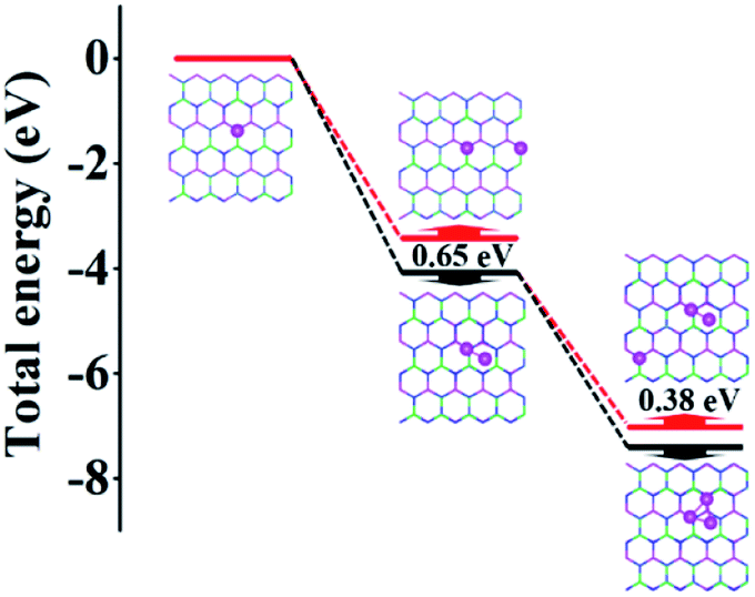 | ||
| Fig. 2 The total energy of Al atoms adsorbed one by one on the Al0.5Ga0.5N surface. | ||
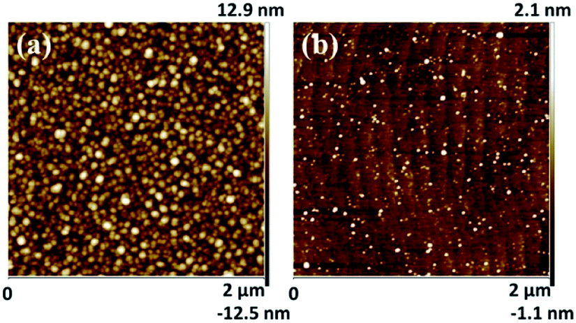
The experiment obtained a similar phenomenon consistent with the calculation results. In this study, four “in situ NP growth” samples were prepared by varying the growth times of 0 s, 15 s, 30 s, and 60 s, named Sample A, B, C, and D, respectively, i.e., Sample A is an AlGaN epi-layer without in situ NPs. Fig. 3 shows the surface morphology of these four samples in an area of 1 μm × 1 μm by using a tapping-mode AFM. A typical stepped surface topography of the AlGaN epi-layer (Sample A) is shown in Fig. 3(a), while nano-islands are shown on the AlGaN layers with in situ grown NP (Sample B, C, and D) as shown in Fig. 3(b–d). Fig. 3(e–h) show the 3D morphologies of Sample A, B, C, and D respectively. The average diameters of NPs on Sample B, C, and D are 20 nm, 40 nm, and 60 nm, respectively. The results show that the diameters of the nano-islands and the thickness of the NP layer increase with the increasing growth time. During the in situ growth process, the Al precursor decomposed and nucleated on the heated substrate. The subsequent Al precursors decomposed and expanded based on these nucleation sites, which is consistent with the evolution of growth kinetics in MOCVD growth by previous studies.33 When the size is enlarged and merged, a quasi-continuous layer would also be formed.
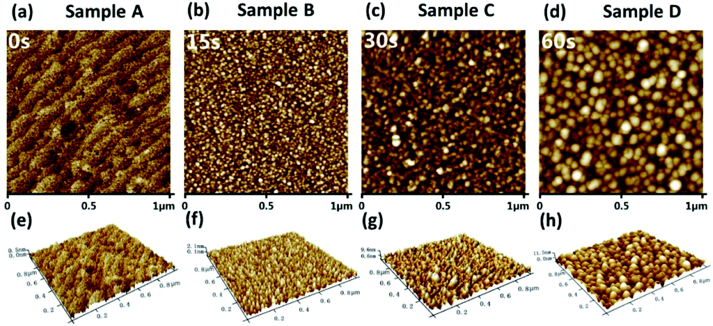 | ||
| Fig. 3 AFM images of the four samples with different in situ NP growth times. (a–d) are the planar views, and (e–h) are the 3D views of the four samples, respectively. | ||
To determine the composition of the surface nano-islands, an XPS test was performed. Fig. 4(a) shows the XPS survey scan spectrum of the sample without NPs, that is, the AlGaN epi-layer, while Fig. 4(b) shows that of the sample with NPs with 30 s in situ growth. Compared with those of the AlGaN epi-layer without NPs, the peaks of N 1s, Ga 3d and Ga 2p core-levels are significantly reduced while O 1s is increased in Fig. 4(b). However, the intensity of the Al 2p core-level peak does not change obviously, which means that there is almost no Ga and N in these NPs, but Al is present. The XPS narrow region scan results of the Al 2p and O 1s core-levels are shown in Fig. 4(c and d). The chemical shift of the Al 2p peak position is distinct, and the binding energy (BE) shifts from 73.3 eV to 74.1 eV correspond to the Al–N bond34 and Al–O bond35 respectively. Moreover, a shoulder located at the left side of the major peak could be observed and might be due to metallic Al (Al–Al bond, at ∼72.9 eV (ref. 36)), indicating that Al-clusters were formed on the AlGaN epi-layers. Fig. 4(d) also indicates the existence of an O–Al bond (∼531.6 eV).37 The XPS spectra demonstrate that the composition of nano-islands could be Al with an oxide film, Al2O3 (usually ∼3 nm).
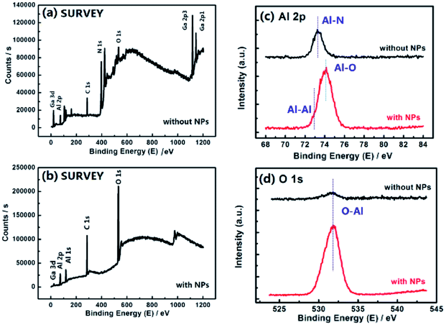 | ||
| Fig. 4 (a and b) are XPS survey scan spectra of the samples with and without surface NPs. (c) is Al 2p core-level XPS spectra, and (d) is O 1s core-level XPS spectra of the samples with and without NPs. | ||
To further verify the existence of Al NPs, the samples with NPs were etched with H3PO4 solution at 65 °C for 10 minutes. Fig. 5(a and b) show the tapping-AFM surface topography of a typical sample with in situ grown NPs for 60 s before and after H3PO4 etching, respectively. The etched sample in Fig. 5(b) shows a significant step shape surface topography, like Sample A in Fig. 3(a), which proves the reaction between the nano-islands and the H3PO4 solution. Considering the growth process in MOCVD, the NPs can be confirmed to be Al nanoparticles again.
 | ||
| Fig. 5 The AFM surface morphology of in situ NP growth samples before (a) and after (b) H3PO4 etching. | ||
Here we use MSM-type AlGaN-based UV PDs to verify the enhancement of in situ grown Al NPs. The schematic of the device structure is shown in the inset of Fig. 6(b). Four PDs (PD A, PD B, PD C and PD D) were fabricated, corresponding to the different in situ Al NP growth times (0 s, 15 s, 30 s, and 60 s). Fig. 6 illustrates the dark current (Idark) and the spectral responsivity under 10 V bias of these detectors. For PD B, with 15 s in situ NP growth, the Idark is slightly lower than that without NPs, which could be attributed to the passivation effect of Al2O3,38 while for PD C (30 s) and PD D (60 s), the Idark is slightly increased due to the lower Schottky contact height between the Ni/Au electrons and the AlGaN epilayer because of the Al NP increase.
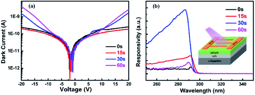 | ||
| Fig. 6 (a) Dark current–voltage (I–V) curves of AlGaN MSM detectors with and without Al NPs. (b) Responsivity of MSM photodetectors with and without Al NPs under 10 V bias. A schematic of the device structure is shown in the inset of (b). | ||
The spectral response of the AlGaN PDs with and without in situ grown Al NPs was also studied. For samples with 0 s and 15 s growth time, the responsivity peaks at approximately 290 nm. And for samples with 30 s and 60 s growth time, the peaks are slightly blue shifted, at 288 nm, which could be related to the plasmon effect of Al on the surface, consistent with the results reported previously.23,39 For the 15 s sample, no significant blue shift occurs in the cut-off wavelength due to the small diameter of the NPs (less than 20 nm).23 As shown in Fig. 6(b), all PDs with in situ grown Al NPs have higher responsivity compared with PDs without NPs. The peak responsivity of PD C (30 s) is enhanced over 9 times that of PD A. Compared with our previous work, in which the responsivity of the AlGaN PD with ex situ Al NPs was enhanced nearly 2 times more than that without Al NPs,23 the in situ preparation of Al NPs is superior. Further deposition of Al induces deterioration in photoresponsivity (PD D). As shown in Fig. 3, the average size of Al NPs increases with the increasing deposition time, indicating the size of Al NPs affects the performance improvement, and the optimized deposition time in the present work is 30 s.
The enhancement of photoresponsivity might have resulted from these possible mechanisms: (i) the in situ Al NP surface plasmon resonance induces local electric field enhancement,21 and thus generates more carriers as well as accelerates the separation of the carriers, leading to the enhancement of the responsivity. (ii) Al NPs generate hot carriers, which are emitted across the Schottky barrier and injected into the conduction band of the AlGaN layer, leading to the photocurrent increase. The hot carrier effect is especially noticeable when the size of the NPs is small.40,41 Therefore, in PD B, the main enhancement mechanism is the hot carrier phenomenon. (iii) The in situ grown NPs and the AlGaN interface have less pollution, which could improve the transfer of energy and carriers from metal NPs to the semiconductor. This might be the main reason for the better improvement of photoresponsivity in this work than in the ex situ prepared Al NPs.
Conclusion
In conclusion, we have verified the feasibility of the in situ growth of Al NPs by MOCVD from both theoretical calculations and experiments, and achieved photoresponsivity enhanced AlGaN-based UV PDs by in situ grown Al NP surface plasmons. The peak photoresponsivity of PDs was enhanced by 9 times more than that of the device without Al NPs at 288 nm under 10 V bias, which is better than the enhancement of AlGaN-based UV PDs by ex situ prepared Al NPs previously. In situ growth of Al NPs not only causes surface plasmon resonance, but also reduces energy and carrier loss at the interface because of less contamination. Our work broadens the application of Al surface plasmon enhanced AlGaN-based UV and DUV photoelectric devices.Conflict of interest
The authors declare no competing financial interest.Acknowledgements
This work was supported by the National Key R&D Program of China [2016YFB0400101], the National Science Fund for Distinguished Young Scholars [61725403], the National Natural Science Foundation of China [61574142, 61874118, 61827813, and 61704171], the Key Program of the International Partnership Program of CAS [181722KYSB20160015], the Jilin Provincial Science & Technology Department [20180201026GX], and the Youth Innovation Promotion Association of CAS.References
- M. Sajjad, W. M. Jadwisienczak and P. Feng, Nanoscale, 2014, 6, 4577–4582 RSC.
- H. Durmaz, D. Nothern, G. Brummer, T. D. Moustakas and R. Paiella, Appl. Phys. Lett., 2016, 108, 201102 CrossRef.
- D. Y. Kim, J. H. Park, J. W. Lee, S. Hwang, S. J. Oh, J. Kim, C. Sone, E. F. Schubert and J. K. Kim, Light: Sci. Appl., 2015, 4, e263 CrossRef CAS.
- T. A. Growden, W. Zhang, E. R. Brown, D. F. Storm, D. J. Meyer and P. R. Berger, Light: Sci. Appl., 2018, 7, 17150 CrossRef CAS PubMed.
- Z. Bryan, I. Bryan, S. Mita, J. Tweedie, Z. Sitar and R. Collazo, Appl. Phys. Lett., 2015, 106, 232101 CrossRef.
- H. Yoshida, Y. T. Akagi, M. Kuwabara, H. Amano and H. Kan, Jpn. J. Appl. Phys., 2007, 46, 5782–5784 CrossRef CAS.
- D. Li, K. Jiang, X. Sun and C. Guo, Adv. Opt. Photonics, 2018, 10, 43–110 CrossRef.
- E. Muñoz, Phys. Status Solidi B, 2007, 244, 2859–2877 CrossRef.
- C.-Y. Cho, Y. Zhang, E. Cicek, B. Rahnema, Y. Bai, R. McClintock and M. Razegh, Appl. Phys. Lett., 2013, 102, 211110 CrossRef.
- S. Butun, N. A. Cinel and E. Ozbay, Nanotechnology, 2012, 23, 444010 CrossRef PubMed.
- V. A. Briand, V. Thilakarathne, R. M. Kasi and C. V. Kumar, Talanta, 2012, 99, 113–118 CrossRef CAS PubMed.
- J. Homola, Chem. Rev., 2008, 108, 462–493 CrossRef CAS PubMed.
- C. Clavero, Nat. Photonics, 2014, 8, 95 CrossRef CAS.
- J. S. Clausen, E. Højlund-Nielsen, A. B. Christiansen, S. Yazdi, M. Grajower, H. Taha, U. Levy, A. Kristensen and N. A. Mortensen, Nano Lett., 2014, 14, 4499–4504 CrossRef CAS PubMed.
- S. J. Tan, L. Zhang, D. Zhu, X. M. Goh, Y. M. Wang, K. Kumar, C.-W. Qiu and J. K. W. Yang, Nano Lett., 2014, 14, 4023–4029 CrossRef CAS PubMed.
- Y. Wu, X. Sun, Y. Jia and D. Li, Chin. Phys. B, 2018, 27, 26101 CrossRef.
- X. Jiao and S. Blair, Opt. Express, 2012, 20, 29909–29922 CrossRef CAS PubMed.
- Y.-H. Su, Y.-F. Ke, S.-L. Cai and Q.-Y. Yao, Light: Sci. Appl., 2012, 1, e14 CrossRef.
- M.-K. Kwon, J.-Y. Kim and S.-J. Park, J. Cryst. Growth, 2013, 370, 124–127 CrossRef CAS.
- D. Li, X. Sun, H. Song, Z. Li, Y. Chen, H. Jiang and G. Miao, Adv. Mater., 2012, 24, 845–849 CrossRef CAS PubMed.
- D. Li, X. Sun, Y. Jia, M. I. Stockman, H. P. Paudel, H. Song, H. Jiang and Z. Li, Light: Sci. Appl., 2017, 6, e17038 CrossRef CAS PubMed.
- N. Gao, K. Huang, J. Li, S. Li, X. Yang and J. Kang, Sci. Rep., 2012, 2, 816 CrossRef PubMed.
- G. Bao, D. Li, X. Sun, M. Jiang, Z. Li, H. Song, H. Jiang, Y. Chen, G. Miao and Z. Zhang, Opt. Express, 2014, 22, 24286 CrossRef CAS PubMed.
- W. Zhang, J. Xu, W. Ye, Y. Li, Z. Qi, J. Dai, Z. Wu, C. Chen, J. Yin, J. Li, H. Jiang and Y. Fang, Appl. Phys. Lett., 2015, 106, 021112 CrossRef.
- O. Lecarme, Q. Sun, K. Ueno and H. Misawa, ACS Photonics, 2014, 1, 538–546 CrossRef CAS.
- G. H. Chan, J. Zhao, G. C. Schatz and R. P. V. Duyne, J. Phys. Chem. C, 2008, 112, 13958–13963 CrossRef CAS.
- A. Boltasseva, J. Opt. A: Pure Appl. Opt., 2009, 11, 114001 CrossRef.
- C.-Y. Cho, Y. Zhang, E. Cicek, B. Rahnema, Y. Bai, R. McClintock and M. Razeghi, Appl. Phys. Lett., 2013, 102, 211110 CrossRef.
- D. L. Winn, M. J. Hale, T. J. Grassman, J. Z. Sexton and A. C. Kummel, J. Chem. Phys., 2007, 127, 134705 CrossRef PubMed.
- V. Barone, M. Casarin, D. Forrer, M. Pavone, M. Sambi and A. Vittadini, J. Comput. Chem., 2009, 30, 934–939 CrossRef CAS PubMed.
- S. Grimme, J. Comput. Chem., 2006, 27, 1787–1799 CrossRef CAS PubMed.
- T. G. Mihopoulos, V. Gupta and K. F. Jensen, J. Cryst. Growth, 1998, 195, 733–739 CrossRef CAS.
- J. Ma, Q. Zhuang, G. Chen, C. Huang, S. Li, H. Wang and J. Kang, J. Phys. Chem. A, 2010, 114, 9028–9033 CrossRef CAS PubMed.
- T. Hagio, A. Takase and S. Umebayashi, J. Mater. Sci. Lett., 1992, 11, 878–880 CrossRef CAS.
- H. He, K. Alberti, T. L. Barr and J. Klinowski, J. Phys. Chem., 1993, 97, 13703–13707 CrossRef CAS.
- C. Hinnen, D. Imbert, J. M. Siffre and P. Marcus, Appl. Surf. Sci., 1994, 78, 219–231 CrossRef CAS.
- B. R. Strohmeier, Surf. Sci. Spectra, 1994, 3, 135–140 CrossRef CAS.
- X. Sun, D. Li, H. Jiang, Z. Li, H. Song, Y. Chen and G. Miao, Appl. Phys. Lett., 2011, 98, 121117 CrossRef.
- J. Yin, Y. Li, S. Chen, J. Li, J. Kang, W. Li, P. Jin, Y. Chen, Z. Wu, J. Dai, Y. Fang and C. Chen, Adv. Opt. Mater., 2014, 2, 451–458 CrossRef CAS.
- P. Christopher and M. Moskovits, Annu. Rev. Phys. Chem., 2017, 68, 17 CrossRef PubMed.
- F. Wang and N. A. Melosh, Nano Lett., 2011, 11, 5426–5430 CrossRef CAS PubMed.
| This journal is © The Royal Society of Chemistry 2020 |