
 Open Access Article
 This Open Access Article is licensed under a
 Creative Commons Attribution 3.0 Unported Licence
Few-layer hexagonal bismuth telluride (Bi2Te3) nanoplates with high-performance UV-Vis photodetection†
Ye
Zhang‡
 a,
Qi
You‡
a,
Weichun
Huang
*b,
Lanping
Hu
b,
Jianfeng
Ju
b,
Yanqi
Ge
*a and
Han
Zhang
*a
a,
Qi
You‡
a,
Weichun
Huang
*b,
Lanping
Hu
b,
Jianfeng
Ju
b,
Yanqi
Ge
*a and
Han
Zhang
*a
aSZU-NUS Collaborative Innovation Centre for Optoelectronic Science & Technology, International Collaborative Laboratory of 2D Materials for Optoelectronics Science and Technology of Ministry of Education, Institute of Microscale Optoelectronics, Shenzhen University, Shenzhen 518060, China. E-mail: hzhang@szu.edu.cn
bNantong Key Lab of Intelligent and New Energy Materials, College of Chemistry and Chemical Engineering, Nantong University, Nantong 226019, Jiangsu, P. R. China
First published on 10th February 2020
Abstract
It is widely known that the excellent intrinsic electronic and optoelectronic advantages of bismuthene and tellurene make them attractive for applications in transistors and logic and optoelectronic devices. However, their poor optoelectronic performances, such as photocurrent density and photoresponsivity, under ambient conditions severely hinder their practical application. To satisfy the demand of high-performance optoelectronic devices and topological insulators, bismuth telluride nanoplates (Bi2Te3 NPs) with different sizes, successfully synthesized by a solvothermal approach have been, for the first time, employed to fabricate a working electrode for photoelectrochemical (PEC)-type photodetection. It is demonstrated that the as-prepared Bi2Te3 NP-based photodetectors exhibit remarkably improved photocurrent density, enhanced photoresponsivity, and faster response time and recovery time in the UV-Vis region, compared to bismuthene and tellurene-based photodetectors. Additionally, the PEC stability measurements show that Bi2Te3 NPs have a comparable long-term stability for on/off switching behaviour for the bismuthene and tellurene-based photodetectors. Therefore, it is anticipated that the present work can provide fundamental acknowledgement of the optoelectronic performance of a PEC-type Bi2Te3 NP-based photodetector, shedding light on new designs of high-performance topological insulator-based optoelectronic devices.
Introduction
The individual elements tellurium (Te) and bismuth (Bi) have been widely applied to the fabrication and applications of photodetectors over the past decade due to their simple composition, excellent nonlinear photonic performance,1–4 and intriguing thermoelectric5–7 and photoelectric properties.8–10 Similar to the famous black phosphorus (BP), both Te and Bi have a layer-dependent energy band gap (Eg)1,3,8 that can be easily tuned (Te: 0.35–1.0 eV;1 Bi: 0–0.55 eV (ref. 3)) when the thickness of Te or Bi decreases from bulk to monolayer. Recently, Ye et al. reported that ultrathin 2D nonlayered Te nanosheets synthesized by a substrate-free solution process, displayed high on/off ratios (106), remarkable field-effect mobility (700 cm2 V−1 s−1) and comparable air-stable performance.8 Besides, the ultrathin Te nanosheets fabricated by a simple liquid phase exfoliation (LPE) method, showed excellent photoresponse behaviors from the UV to the visible region in association with strong time and cycle stability for the on/off switching behaviors.10 In 2017, Zhang et al. reported that ultrasmall Bi quantum dots fabricated by a LPE approach, exhibited good photoresponse performance from the UV to visible region as well as long-term photoresponse stability.11 Nevertheless, the poor photoresponse performances of Te or Bi nanomaterials, especially photoelectrochemical (PEC) photocurrent density and photoreponsivity, still severely limit their device development for practical applications. Therefore, it is still a challenge to explore a new method to improve their photoresponse performance under ambient conditions.However, bismuth telluride (Bi2Te3), basically known as a compound of the post-transition metal element Bi and the non-metal element Te, also exhibits a thickness-dependent Eg (from 0.16 eV to 1.36 eV),12,13 and a high structural stability.14,15 Versatile strategies have already been employed to synthesize Bi2Te3 nanomaterials, including template synthesis,16 evaporation,17 electrochemical deposition,18 chemical solution process,19,20 solvothermal approaches21,22 and microwave-assisted methods.23 Bi2Te3 as one of the common topological insulators, features an unconventional phase of quantum matter possessing an insulating bulk state as well as a metallic surface state.17 Such metallic surface states were experimentally evidenced to be protected by time-reversal symmetry and demonstrated to be robust against non-magnetic perturbation.24,25 In addition, topological insulator Bi2Te3 exhibits an excellent surface mobility26 and good optoelectronic performance.27 This, combined with the relatively narrow Eg of Bi2Te3 and low cost and facile synthesis of Bi2Te3 nanomaterials, has drawn great interest in photodetection,28–30 field effect transistors,26,31 spintronics,32,33 thermoelectrics,22,34 and lasers.35–37 These advantages of Bi2Te3 merit it to be qualified for the practical application in high-performance optoelectronic devices.
In this work, Bi2Te3 nanoplates (NPs) with a rhombohedral phase in the space group D53d(R3m), have been successfully synthesized by a solvothermal approach. To determine the size-dependent PEC performances of Bi2Te3 NPs, different sizes of Bi2Te3 NPs were readily obtained by simply tuning the reaction time. The as-synthesized Bi2Te3 NPs were, for the first time, developed as working materials to fabricate a PEC-type photodetector in various electrolytes. The PEC results demonstrate that the Bi2Te3 NP-based photodetectors exhibit not only a largely improved photocurrent density and photoresponsivity, but also a comparable photoresponse stability compared to that of Bi or Te nanomaterial-based photodetectors. It is anticipated that this work can provide fundamental guidance for constructing high-performance Bi2Te3 NP-based photodetectors, paving the way to new designs of topological insulator-based optoelectronic devices with excellent properties.
Methods
Materials
Poly(vinyl pyrrolidone) (PVP, K30), poly(vinylidene fluoride) (PVDF, Mw = 534![[thin space (1/6-em)]](https://www.rsc.org/images/entities/char_2009.gif) 000 g mol−1), Bi(NO3)3·5H2O, dimethyl formamide (DMF, 99.9%), acetone, and ethanol were purchased from Sigma-Aldrich. Sodium tellurite (Na2TeO3, 99.9%) and indium tin oxide (ITO) were purchased from Aladdin Co., Inc. All chemical reagents were used without further purification. Double-distilled deionized (DI) water was used for synthesis.
000 g mol−1), Bi(NO3)3·5H2O, dimethyl formamide (DMF, 99.9%), acetone, and ethanol were purchased from Sigma-Aldrich. Sodium tellurite (Na2TeO3, 99.9%) and indium tin oxide (ITO) were purchased from Aladdin Co., Inc. All chemical reagents were used without further purification. Double-distilled deionized (DI) water was used for synthesis.
Synthesis of Bi2Te3 hexagonal NPs
In a typical procedure, 20 mmol Bi(NO3)3·5H2O and 40 mmol Na2TeO3 were first dissolved in 30 mL DI water. Then 0.03 mmol PVP was added into the solution and it was kept stirring for 30 min to form a homogeneous mixture. The mixture was transferred into a 50 mL Teflon-lined autoclave and placed in an oven at 180 °C. After a predetermined reaction time (2 h or 12 h), the reaction was stopped by quenching the system to room temperature. The Bi2Te3 hexagonal NPs were obtained by centrifugation at 4000 rpm for 20 min and washed with deionized water, ethanol and acetone, each. The product was finally dried in a vacuum oven at 80 °C overnight for the next use.Characterization
The morphologies and dimensions of Bi2Te3 NPs were determined by both scanning electron microscopy (SEM, Hitachi-SU8010) and transmission electron microscopy (TEM, FEI Tecnai G2 F30). High-resolution TEM (HRTEM) was performed to determine the atomic arrangements of the as-synthesized Bi2Te3 NPs. Energy-dispersive X-ray spectroscopy (EDS) was carried out using an FEI Tecnai G2 F30 TEM equipped with an Oxford EDAX EDS system. Atomic force microscopy (AFM, Bruker, with 512 pixels per line) was performed after depositing a drop of dispersion onto a silicon substrate. The X-ray diffraction (XRD) analysis was performed on an X'Pert-Pro MPD diffractometer with a Cu K-α radiation source at room temperature. Ultraviolet-visible (UV-Vis) absorption spectroscopy was performed with a spectral range of 200–1500 nm by using a UV-Vis absorbance spectrometer (Cary 60, Agilent) at room temperature.Photoresponse activity
The PEC measurement system in Scheme S1† was used to characterize the photoresponse behaviour of Bi2Te3 NPs. A standard three-electrode system, that is, a working electrode (for example, Bi2Te3 NPs deposited on ITO-coated glass, photoanode), a counter electrode (platinum wire, photocathode), and a reference electrode (Ag/AgCl electrode), was assembled in various aqueous electrolytes, including KOH (0.1 M, 0.5 M, and 1.0 M), KCl (0.5 M), and HCl (0.5 M). To ensure good adhesion between ITO-coated glass and the sample, the as-synthesized samples were first re-dispersed in a 0.2 mg mL−1 PVDF/DMF solution, and then the dispersion was deposited onto ITO-coated glass and dried under vacuum at 80 °C overnight. Electrochemical impedance spectra (EIS) were obtained in the frequency range from 1 to 105 Hz with an amplitude of 0.005 V. Amperometric current–time (I–t) curves were recorded at bias voltages of 0 V, 0.3 V, and 0.6 V with increasing power densities at a sampling interval of 5 s. Simulated light (300–800 nm) and lasers with different λ (λ = 365 nm, 400 nm, 475 nm, 550 nm, 600 nm and 700 nm) were employed to irradiate the Bi2Te3 NP-based photodetectors. Light power densities (Pλ) of these irradiations with labels of Dark, I, II, III, IV, and VI levels gradually increased (Table S1†). As a control experiment, a piece of naked ITO-coated glass was also irradiated by using a SL under the same conditions.Results and discussion
The Bi2Te3 NPs with a well-defined hexagonal shape were synthesized by the solvothermal method. In order to investigate the influence of the size of Bi2Te3 NPs on photoresponse performances, two kinds of Bi2Te3 NPs with different sizes have been facilely synthesized by tuning the reaction time. For convenience, the Bi2Te3 NPs reacted after 2 h and 12 h are abbreviated as Bi2Te3 NPs-1 and Bi2Te3 NPs-2, respectively. Fig. 1a and b give the SEM images of the as-prepared Bi2Te3 NPs-1 and Bi2Te3 NPs-2, both of which exhibit a well-defined hexagonal shape, while the average lateral dimensions of Bi2Te3 NPs-1 and Bi2Te3 NPs-2 are 620 ± 150 nm and 730 ± 210 nm, respectively. The TEM characterization (Fig. 1c and d) reveals that the as-prepared Bi2Te3 NPs also represent a well-defined hexagonal shape. Besides, Bi2Te3 NPs-2 have darker hexagons (Fig. 1d), compared to Bi2Te3 NPs-1 (Fig. 1c), indicating that the longer the reaction time the thicker the Bi2Te3 NPs are, which is in good agreement with the “oriented attachment” mechanism of Bi2Te3 NPs.38,39 The HRTEM image (Fig. 1e) shows a clear lattice spacing of 0.22 nm, consistent with the (1120) plane of layered Bi2Te3.27 Sharp diffraction spots are observed in the selected area electron diffraction (SAED) pattern (Fig. 1f), and the EDS line scan analysis (Fig. 1g) reveals compositional variation in a single Bi2Te3 NP, suggesting that Bi and Te are evenly distributed (Fig. 1h and j).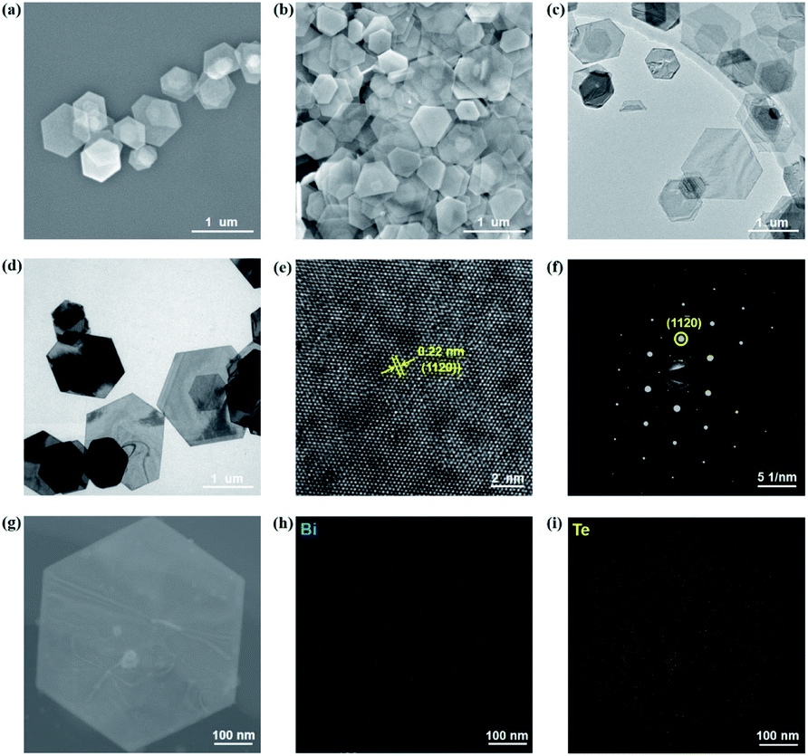 | ||
| Fig. 1 Structural characterization of the as-prepared Bi2Te3 NPs. SEM images of (a) Bi2Te3 NPs-1 and (b) Bi2Te3 NPs-2. TEM images of (c) Bi2Te3 NPs-1 and (d) Bi2Te3 NPs-2. (e) HRTEM image of Bi2Te3 NPs-1. (f) SAED pattern of Bi2Te3 NPs-1. (g) TEM image of one single hexagonal Bi2Te3 NP and results of its EDS elemental mapping of (h) Bi and (i) Te shown in (g). | ||
The thicknesses of the as-synthesized Bi2Te3 NPs-1 and Bi2Te3 NPs-2 were characterized by AFM, as shown in Fig. 2a and b, respectively. It can be clearly seen in Fig. 2c and d that with the increase in the reaction time, the measured thickness of Bi2Te3 NPs obviously increases from 11.1 nm to 17.2 nm, which correspond to 11 and 17 layers, respectively, given that one layer is regarded as an average quintuple layer of Te–Bi–Te–Bi–Te with a thickness of 1.0 nm.17 XRD patterns of the as-synthesized Bi2Te3 NPs, as shown in Fig. 2e, can be indexed to a rhombohedral Bi2Te3 structure (JCPDS Card Number 15-0863). UV-Vis absorption spectroscopy was employed to characterize the optical response of differently sized Bi2Te3 NPs (Fig. 2f). Broadband absorption from 260 nm to 1500 nm, is observed for Bi2Te3 NPs-1 and Bi2Te3 NPs-2, which is in good agreement with previously reported results,40,41 implying great potential for application in broadband optoelectronic devices. Besides, Tauc plots of Bi2Te3 NPs-1 and Bi2Te3 NPs-2 (Fig. 1g) were calculated based on the results in Fig. 1f, and size-dependent Eg values of 0.83 eV (Bi2Te3 NPs-1) and 1.0 eV (Bi2Te3 NPs-2) were obtained, close to that of the previously reported Bi2Te3 nanoparticles,42 suggesting that the Eg of Bi2Te3 NPs could be easily controlled by simply tuning the reaction conditions.
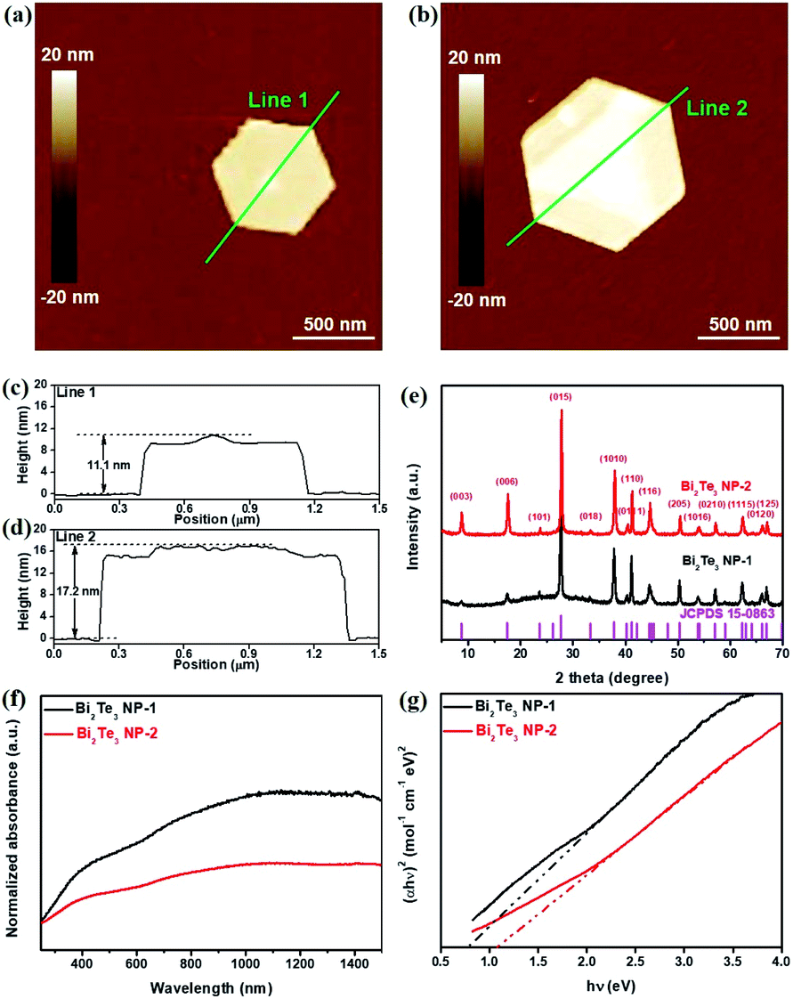 | ||
| Fig. 2 AFM images of (a) Bi2Te3 NPs-1 and (b) Bi2Te3 NPs-2. (c, d) Height profiles along the green lines in (a) and (b), respectively. (e) XRD patterns of Bi2Te3 NPs-1 and Bi2Te3 NPs-2. (f) UV-Vis spectra of the as-prepared Bi2Te3 NPs-1 and Bi2Te3 NPs-2 and (g) their Tauc plots for the calculations of Eg. | ||
The typical photoresponse behaviour of the Bi2Te3 NP-based photodetector was evaluated using a PEC system equipped with a standard three-electrode configuration, as shown in Scheme S1.†Fig. 3a gives the patterns of the as-fabricated Bi2Te3 NPs cast onto ITO-coated glass, exhibiting strong on/off switching photoresponse behaviours at an applied bias voltage of 0.6 V. For clarity, the profile of the naked ITO-coated glass was added in Fig. 3a, which displays a negligible signal as compared to Bi2Te3 NPs under the same conditions, revealing that the photoresponse signal indeed comes from the Bi2Te3 NPs rather than ITO. In addition, it should be noted that the type of electrolytes plays an important role in the PEC performance. As is shown in Fig. 3b, c and e, Bi2Te3 NPs-2 irradiated by using several single-wavelength lasers, exhibit an excellent on/off switching photoresponse behaviour in 0.5 M KCl (Fig. 3c) and 0.5 M KOH (Fig. 3e) while they show poor performance in 0.5 M HCl (Fig. 3b) at 0.6 V, suggesting that KCl and KOH are preferred electrolytes for Bi2Te3 NPs in this PEC system but HCl is not. Besides, the influences of lasers with different λ and Pλ on the PEC performance were investigated (Fig. 3c–f). Six lasers with specific λ (λ = 365, 400, 475, 550, 650, and 700 nm) and Pλ were employed to demonstrate the laser wavelength-dependent PEC performance of Bi2Te3 NPs. Similarly, the profiles of naked ITO-coated glass irradiated by using a SL are also added for comparison in Fig. 3c–f. It can be observed that when the λ value is less than 550, Bi2Te3 NPs show a strong PEC signal in KCl and KOH and the signal gradually increases with the decrease of the λ value (Fig. 3c–f), which can be attributed to the relatively highe laser energy and Pλ (Table S1†). However, when λ ≥ 550 nm, a negligible photoresponse signal of Bi2Te3 NPs can be observed, different from the results in absorption spectra, which is attributed to the very weak laser energy employed for PEC measurements in this work. In addition, it should be pointed out that the signal of naked ITO-coated glass irradiated by using a SL with much higher Pλ is obviously lower than that of Bi2Te3 NPs (Fig. 3c–f) irradiated by using single-wavelength lasers with shorter λ, e.g., 365 nm, while higher than that irradiated by using single-wavelength lasers with longer λ, e.g., 650 nm and 700 nm, reconfirming the truth of the PEC signal of Bi2Te3 NPs. Furthermore, it shows the same trend when the Pλ gradually increases from dark to VI in both KCl and KOH, that is, the PEC signal of Bi2Te3 NPs increases with the Pλ (Fig. 3c–f). To quantitatively evaluate the photoresponse performance of Bi2Te3 NPs, the photocurrent density (Pph) and photoresponsivity (Rph) can be obtained by:43,44
| Pph = (Ilight − Idark)/S | (1) |
| Rph = Pph/Pλ | (2) |
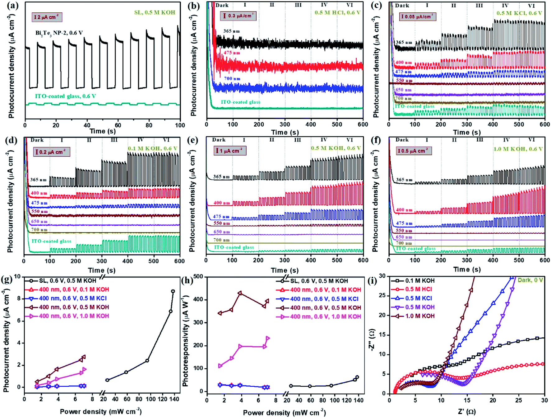 | ||
| Fig. 3 The photoresponse behaviours of Bi2Te3 NP-2-based photodetectors in various electrolytes under a SL and light with various wavelengths. (a) The on/off switching behaviours triggered by a SL in 0.5 M KOH at 0.6 V at 134 mW cm−2. (b–f) The on/off switching behaviours in various electrolytes under light with wavelengths of 365, 400, 475, 550, 650, and 700 nm at 0.6 V in (b) 0.5 M HCl, (c) 0.5 M KCl, (d) 0.1 M KOH, (e) 0.5 M KOH, and (f) 1.0 M KOH. For clarity, the photoresponse profile of naked ITO-coated glass irradiated by using a SL was added. (g) Pph as a function of light power density under a SL and light with various wavelengths. (h) Rph as a function of light power density under a SL and irradiation with various wavelengths. (i) EIS patterns of Bi2Te3 NPs-2 in various electrolytes under dark environments at 0.6 V. | ||
Due to the size-dependent Eg of Bi2Te3 NPs (Fig. 2g), the photoresponse behaviours of the Bi2Te3 NPs-1 and Bi2Te3 NPs-2 irradiated by using a SL and three kinds of lasers (365, 400, and 475 nm) were studied to understand the influence of the size of Bi2Te3 NPs on the PEC performance, as shown in Fig. 4. It can be seen that the PEC signals of both Bi2Te3 NPs-1 and Bi2Te3 NPs-2 increase with the Pλ (Fig. 4a) and show the same trend as those of the Bi2Te3 NPs-2, i.e., the PEC signal declines as the λ value increases (Fig. 4b). In addition, it is noted that the PEC signal of Bi2Te3 NPs-2 is obviously stronger than that of Bi2Te3 NPs-1, no matter which laser was employed (Fig. 4a and b), e.g., the Pph of Bi2Te3 NPs-2 irradiated by using a 400 nm laser at 4.65 mW cm−2 is 2.52 μA cm−2 while that of Bi2Te3 NPs-1 is only 0.729 μA cm−2. This could be attributed to the synergistic effect of the suitable Eg and the number of accessible active sites on the Bi2Te3 NPs-2. Since the Eg of Bi2Te3 NPs inversely correlates with size, the larger Bi2Te3 NPs-1 have stronger absorption under incident light. However, with the size decrease of Bi2Te3 NPs, the specific surface area becomes higher and accessible active sites on the PEC performance of Bi2Te3 NP-based photodetectors, similar to previously reported results.10,44,50 Therefore, the size of nanomaterials has a great influence on the PEC performance; Bi2Te3 NPs tend to be larger, resulting in higher efficiency, which provides fundamental acknowledgement of the design and optimization of PEC-type devices.
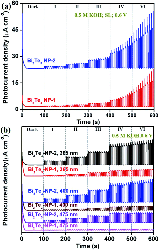 | ||
| Fig. 4 Size effect of Bi2Te3 NPs on the photoresponse performance in 0.5 M KOH under (a) a SL and (b) three different lasers (365, 400, and 475 nm). | ||
In addition, the response time (tres) and recovery time (trec) of the Bi2Te3 NP-based photodetector were ascribed to the time interval for the rise and decay from 10% to 90% and from 90% to 10% of its peak value, respectively.48,51 It can be observed that regardless of the size of Bi2Te3 NPs and the type of electrolytes, the Bi2Te3 NP-based photodetector always shows fast tres (0.001–0.09 s) as well as trec (0.001–0.07 s) (Fig. 5), both of which are superior to those of the bismuthene-based photodetector (tres = 0.2 s, trec = 0.2 s),11 tellurene-based photodetector (tres = 0.2 s, trec = 0.2 s),10 ZnO homojunction nanowires (tres = ∼50 s, trec = ∼200 s)46 and GaN nanowires (tres = 0.003 s, trec = 0.003 s).47 This could be attributed to the unconventional phase of Bi2Te3 quantum matter. This indicates that the Bi2Te3 NP-based photodetector has appealing potential in the field of PEC-type devices.
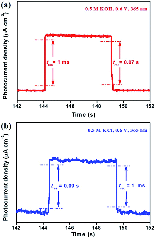 | ||
| Fig. 5 The tres and trec of (a) Bi2Te3 NPs-1 in 0.5 M KOH and (b) Bi2Te3 NPs-2 in 0.5 M KCl, irradiated by using a 365 nm laser. | ||
Long-term stability measurements of the photoresponse of Bi2Te3 NP-based photodetectors are of great importance for practical application. Fig. 6 gives the stability profiles of the Bi2Te3 NP-1-based photodetector irradiated by using a SL in 0.1 M KOH at a bias voltage of 0.6 V. The 600 cycles with 5 s intervals of on/off switching were traced (Fig. 6a), and the 481–500th cycles were chosen to evaluate the PEC stability of the Bi2Te3 NP-1-based photodetector (Fig. 6b). It should be pointed out that no obvious change is observed by visual inspection of Bi2Te3 NPs-1 specimens after PEC stability measurements in 0.1 M KOH (Fig. S3†), indicating the excellent PEC stability of the as-fabricated Bi2Te3 NP-1-based photodetector. A notable on/off switching behaviour can be observed even after one month, suggesting the long-term PEC stability of Bi2Te3 NPs under ambient conditions. Furthermore, it is calculated from Fig. 6b that the Pphs of the fresh Bi2Te3 NPs-1 in the 481–500th cycles is 879 nA cm−2 in 0.1 M KOH, declining to 439 nA cm−2 after one month. An approximate reduction of 50.1% of Pph was obtained, comparable to that of the bismuthene-based photodetector11 and tellurene-based photodetector.10 The decline of Pph could be ascribed to the weak electrochemical reaction at high bias voltage (0.6 V) under a SL with high Pλ (134 mW cm−2) and slight peel-off during long-running measurements, which can be efficiently solved by coating conductive polymers, such as polyaniline and polypyrrole, onto the surface of Bi2Te3 NPs to remarkably lower the electrochemical reaction of Bi2Te3 NPs and employ stronger binders to make Bi2Te3 NPs more strongly fixed on the surface of ITO-coated glass to avoid the slight peel-off during long-running measurements.
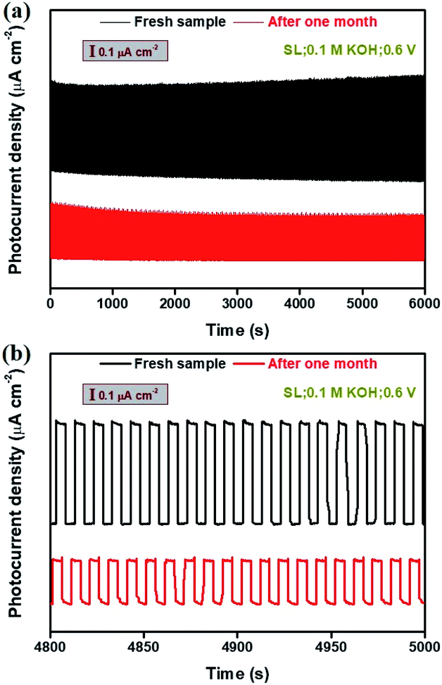 | ||
| Fig. 6 Long-term stability of the photoresponse performance of the Bi2Te3 NPs-1 under a SL in 0.1 M KOH (a) before and (b) after one month. | ||
Conclusions
In summary, topological insulator Bi2Te3 NPs were successfully synthesized by a solvothermal approach and the size of Bi2Te3 NPs can be readily controlled by simply tuning the reaction time. The hexagonal structure of Bi2Te3 NPs was well-characterized, and UV-Vis spectra revealed a broadband absorption range from 260 nm to 1500 nm. The as-synthesized Bi2Te3 NPs were, for the first time, employed as a working material in a PEC-type photodetector. The PEC result not only shows that the Pph and Rph significantly improve but also exhibits faster tres and trec, compared to those of bismuthene-based or tellurene-based photodetectors. It was also shown that Bi2Te3 NPs-2 displayed better PEC performance, attributed to the synergistic effect of optical absorbance and the number of accessible active sites on a Bi2Te3 NP. In addition, good PEC stability of the Bi2Te3 NP-based photodetector was obtained in 0.1 M KOH after one month without any protection, comparable to the bismuthene-based or tellurene-based photodetector. Because of the facile synthesis, easy size control of Bi2Te3 NPs, excellent photoresponse performance, and good long-term stability of the Bi2Te3 NP-based photodetector, we believe that Bi2Te3 can pave a new way for the design of bismuthene or tellurene nanomaterial-based high-performance PEC-type devices with practical applicability.Conflicts of interest
There are no conflicts to declare.Acknowledgements
This research was supported by the National Natural Science Foundation of China (Grant Nos 61805147, 61435010, and 61675135), and the Science and Technology Innovation Commission of Shenzhen (Grant No. JCYJ20180305125141661, and KQTD2015032416270385).References
- L. Wu, W. Huang, Y. Wang, J. Zhao, D. Ma, Y. Xiang, J. Li, J. S. Ponraj, S. C. Dhanabalan and H. Zhang, Adv. Funct. Mater., 2019, 29, 1806346 CrossRef.
- L. Lu, Z. Liang, L. Wu, Y. Chen, Y. Song, S. C. Dhanabalan, J. S. Ponraj, B. Dong, Y. Xiang, F. Xing, D. Fan and H. Zhang, Laser Photonics Rev., 2018, 12, 1700221 CrossRef.
- L. Lu, W. Wang, L. Wu, X. Jiang, Y. Xiang, J. Li, D. Fan and H. Zhang, ACS Photonics, 2017, 4, 2852–2861 CrossRef CAS.
- L. Lu, X. Tang, R. Cao, L. Wu, Z. Li, G. Jing, B. Dong, S. Lu, Y. Li, Y. Xiang, J. Li, D. Fan and H. Zhang, Adv. Optical Mater., 2017, 5, 1700301 CrossRef.
- S. Lin, W. Li, Z. Chen, J. Shen, B. Ge and Y. Pei, Nat. Commun., 2016, 7, 10287 CrossRef CAS PubMed.
- L. Yang, Z.-G. Chen, M. S. Dargusch and J. Zou, Adv. Energy Mater., 2018, 8, 1701797 CrossRef.
- A. Boukai, K. Xu and J. R. Heath, Adv. Mater., 2006, 18, 864–869 CrossRef CAS.
- Y. Wang, G. Qiu, R. Wang, S. Huang, Q. Wang, Y. Liu, Y. Du, W. A. Goddard III, M. J. Kim, X. Xu, P. D. Ye and W. Wu, Nat. Electron., 2018, 1, 228–236 CrossRef.
- W. Wu, G. Qiu, Y. Wang, R. Wang and P. Ye, Chem. Soc. Rev., 2018, 47, 7203–7212 RSC.
- Z. Xie, C. Xing, W. Huang, T. Fan, Z. Li, J. Zhao, Y. Xiang, Z. Guo, J. Li, Z. Yang, B. Dong, J. Qu, D. Fan and H. Zhang, Adv. Funct. Mater., 2018, 28, 1705833 CrossRef.
- C. Xing, W. Huang, Z. Xie, J. Zhao, D. Ma, T. Fan, W. Liang, Y. Ge, B. Dong, J. Li and H. Zhang, ACS Photonics, 2018, 5, 621–629 CrossRef CAS.
- Y. L. Chen, J. G. Analytis, J.-H. Chu, Z. K. Liu, S.-K. Mo, X. L. Qi, H. J. Zhang, D. H. Lu, X. Dai, Z. Fang, S. C. Zhang, I. R. Fisher, Z. Hussain and Z.-X. Shen, Science, 2009, 325, 178–181 CrossRef CAS PubMed.
- Z. Rashid, A. S. Nissimagoudar and W. Li, Phys. Chem. Chem. Phys., 2019, 21, 5679–5688 RSC.
- R. Singh, M. D. Anoop, R. K. Rathore, A. S. Verma, K. Awasthi, V. K. Saraswat and M. Kumar, Appl. Phys. A, 2018, 124, 558 CrossRef.
- J. L. Zhang, S. J. Zhang, J. L. Zhu, Q. Q. Liu, X. C. Wang, C. Q. Jin and J. C. Yu, Phys. B, 2017, 521, 13–16 CrossRef CAS.
- S. A. Sapp, B. B. Lakshmi and C. R. Martin, Adv. Mater., 1999, 11, 402–404 CrossRef CAS.
- D. Kong, W. Dang, J. J. Cha, H. Li, S. Meister, H. Peng, Z. Liu and Y. Cui, Nano Lett., 2010, 10, 2245–2250 CrossRef CAS PubMed.
- A. L. Prieto, M. S. Sander, M. S. Martín-González, R. Gronsky, T. Sands and A. M. Stacy, J. Am. Chem. Soc., 2001, 123, 7160–7161 CrossRef CAS PubMed.
- T. Sun, X. B. Zhao, T. J. Zhu and J. P. Tu, Mater. Lett., 2006, 60, 2534–2537 CrossRef CAS.
- H. Mamur, O. F. Dilmac, H. Korucu and M. R. A. Bhuiyan, Micro Nano Lett., 2018, 13, 1117–1120 CrossRef CAS.
- Y. Liu, Q. Wang, J. Pan, Y. Sun, L. Zhang and S. Song, Chem.–Eur. J., 2018, 24, 9765–9768 CrossRef CAS PubMed.
- G. Zhang, B. Kirk, L. A. Jauregui, H. Yang, X. Xu, Y. P. Chen and Y. Wu, Nano Lett., 2012, 12, 56–60 CrossRef CAS PubMed.
- B. Zhou, Y. Zhao, L. Pu and J.-J. Zhu, Mater. Chem. Phys., 2006, 96, 192–196 CrossRef CAS.
- Z. Alpichshev, J. G. Analytis, J.-H. Chu, I. R. Fisher, Y. L. Chen, Z. X. Shen, A. Fang and A. Kapitulnik, Phys. Rev. Lett., 2010, 104, 016401 CrossRef PubMed.
- T. Zhang, P. Cheng, X. Chen, J.-F. Jia, X. Ma, K. He, L. Wang, H. Zhang, X. Dai, Z. Fang, X. Xie and Q.-K. Xue, Phys. Rev. Lett., 2009, 103, 266803 CrossRef PubMed.
- J. Gooth, B. Hamdou, A. Dorn, R. Zierold and K. Nielsch, Appl. Phys. Lett., 2014, 104, 243115 CrossRef.
- H. Qiao, J. Yuan, Z. Xu, C. Chen, S. Lin, Y. Wang, J. Song, Y. Liu, Q. Khan, H. Y. Hoh, C.-X. Pan, S. Li and Q. Bao, ACS Nano, 2015, 9, 1886–1894 CrossRef CAS PubMed.
- A. Parbatani, E. S. Song, J. Claypoole and B. Yu, Nanotechnology, 2019, 30, 165201 CrossRef CAS PubMed.
- A. Sharma, A. K. Srivastava, T. D. Senguttuvan and S. Husale, Sci. Rep., 2017, 7, 17911 CrossRef PubMed.
- J. Liu, Y. Li, Y. Song, Y. Ma, Q. Chen, Z. Zhu, P. Lu and S. Wang, Appl. Phys. Lett., 2017, 110, 141109 CrossRef.
- H. Liu and P. D. Ye, Appl. Phys. Lett., 2011, 99, 052108 CrossRef.
- G. Xiao, C. Zhu, Y. Ma, B. Liu, G. Zou and B. Zou, Angew. Chem., Int. Ed., 2014, 53, 729–733 CrossRef CAS PubMed.
- R. Dey, T. Pramanik, A. Roy, A. Rai, S. Guchhait, S. Sonde, H. C. P. Movva, L. Colombo, L. F. Register and S. K. Banerjee, Appl. Phys. Lett., 2014, 104, 223111 CrossRef.
- L. Yang, Z.-G. Chen, M. Hong, G. Han and J. Zou, ACS Appl. Mater. Interfaces, 2015, 7, 23694–23699 CrossRef CAS PubMed.
- P. Yan, R. Lin, H. Chen, H. Zhang, A. Liu, H. Yang and S. Ruan, IEEE Photonics Technol. Lett., 2015, 27, 264 CAS.
- H. Mu, Z. Wang, J. Yuan, S. Xiao, C. Chen, Y. Chen, Y. Chen, J. Song, Y. Wang, Y. Xue, H. Zhang and Q. Bao, ACS Photonics, 2015, 2, 832–841 CrossRef CAS.
- Y. Chen, M. Wu, P. Tang, S. Chen, J. Du, G. Jiang, Y. Li, C. Zhao, H. Zhang and S. Wen, Laser Phys. Lett., 2014, 11, 055101 CrossRef.
- J. Song, F. Xia, M. Zhao, Y. L. Zhong, W. Li, K. P. Loh, R. A. Caruso and Q. Bao, Chem. Mater., 2015, 27, 3471–3482 CrossRef CAS.
- G. Zhang, W. Wang, X. Lu and X. Li, Cryst. Growth Des., 2009, 9, 145–150 CrossRef CAS.
- B. K. Gupta, R. Sultana, S. Singh, V. Singh, G. Awana, A. Gupta, B. Singh, A. K. Srivastava, O. N. Srivastava, S. Auluck and V. P. S. Awana, Sci. Rep., 2018, 8, 9205 CrossRef PubMed.
- M. Zhao, J. Zhang, N. Gao, P. Song, M. Bosman, B. Peng, B. Sun, C.-W. Qiu, Q.-H. Xu, Q. Bao and K. P. Loh, Adv. Mater., 2016, 28, 3138–3144 CrossRef CAS PubMed.
- P. Srivastava and K. Singh, J. Exp. Nano., 2014, 9, 1064–1074 CrossRef CAS.
- W. Huang, X. Jiang, Y. Wang, F. Zhang, Y. Ge, Y. Zhang, L. Wu, D. Ma, Z. Li, R. Wang, Z. N. Huang, X. Dai, Y. Xiang, J. Li and H. Zhang, Nanoscale, 2018, 10, 20540–20547 RSC.
- W. Huang, Z. Xie, T. Fan, J. Li, Y. Wang, L. Wu, D. Ma, Z. Li, Y. Ge, Z. N. Huang, X. Dai, Y. Xiang, J. Li, X. Zhu and H. Zhang, J. Mater. Chem. C, 2018, 6, 9582–9593 RSC.
- W. Huang, C. Xing, Y. Wang, Z. Li, L. Wu, D. Ma, X. Dai, Y. Xiang, J. Li, D. Fan and H. Zhang, Nanoscale, 2018, 10, 2404–2412 RSC.
- C.-L. Hsu, Y.-D. Gao, Y.-S. Chen and T.-J. Hsueh, ACS Appl. Mater. Interfaces, 2014, 6, 4277–4285 CrossRef CAS PubMed.
- X. Wang, Y. Zhang, X. Chen, M. He, C. Liu, Y. Yin, X. Zou and S. Li, Nanoscale, 2014, 6, 12009–12017 RSC.
- W. Huang, Y. Zhang, Q. You, P. Huang, Y. Wang, Z. N. Huang, Y. Ge, L. Wu, Z. Dong, X. Dai, Y. Xiang, J. Li, X. Zhang and H. Zhang, Small, 2019, 15, 1900902 CrossRef PubMed.
- X. Ren, Z. Li, Z. Huang, D. Sang, H. Qiao, X. Qi, J. Li, J. Zhong and H. Zhang, Adv. Funct. Mater., 2017, 27, 1606834 CrossRef.
- C. Backes, B. M. Szydłowska, A. Harvey, S. Yuan, V. Vega-Mayoral, B. R. Davies, P.-L. Zhao, D. Hanlon, E. J. G. Santos, M. I. Katsnelson, W. J. Blau, C. Gadermaier and J. N. Coleman, ACS Nano, 2016, 10, 1589–1601 CrossRef CAS PubMed.
- Z. Li, H. Qiao, Z. Guo, X. Ren, Z. Huang, X. Qi, S. C. Dhanabalan, J. S. Ponraj, D. Zhang, J. Li, J. Zhao, J. Zhong and H. Zhang, Adv. Funct. Mater., 2018, 28, 1705237 CrossRef.
Footnotes |
| † Electronic supplementary information (ESI) available. See DOI: 10.1039/d0na00006j |
| ‡ Equal first-author contributions. |
| This journal is © The Royal Society of Chemistry 2020 |