
 Open Access Article
 This Open Access Article is licensed under a Creative Commons Attribution-Non Commercial 3.0 Unported Licence
A carbon nanotube–graphene nanoribbon seamless junction transistor†
Abhay A.
Sagade
 * and
Ameya
Nyayadhish
* and
Ameya
Nyayadhish
Laboratory for Advanced Nanoelectronic Devices, Department of Physics & Nanotechnology, SRM Institute of Science and Technology, Sir C. V. Raman Research Park, Kattankulathur 603 203, India. E-mail: abhaysagade03@gmail.com
First published on 30th January 2020
Abstract
The nature and type of intramolecular junctions are very important for nanoelectronics. Here, a new way of fabricating seamless junctions between carbon nanotubes and graphene nanoribbons (GNRs) is demonstrated. Dielectrophoretically aligned multi-walled carbon nanotubes (CNTs) across metal electrodes are etched with an Ar ion beam at low pressure. We show that grounding of metal electrodes plays an important role in the etching of CNTs in contact with the metal electrodes. If electrodes are grounded, that portion of the CNT doesn't get etched due to the discharge of ions through the ground, and CNT to GNR conversion occurs in the gap region between the metal electrodes. Thus produced GNRs have a large aspect ratio of ∼90, and Raman spectroscopy analysis shows that the distance between the defects is ∼65 nm. The CNT–GNR–CNT seamless junctions are ohmic in nature and the transistor shows a current on/off ratio of 27 with a hole mobility of 350 cm2 V−1 s−1.
Introduction
Carbon nanotubes (CNTs) and graphene are two most important carbon allotropes that have been explored extensively in the field of nanoscience and nanotechnology. Theorists have predicted innovative properties of CNT–graphene intramolecular junctions and proposed new devices for magnetic memory, spintronics, diodes and transistors.1,2 These junctions are also known to host a few quantum phenomena.3 By using DFT calculations Leem et al. have predicted that a CNT–GNR junction based tunnel transistor can show sub-threshold swings of ∼20 mV dec−1.4 However, experimentally there are only a few attempts to fabricate these types of junction devices on the molecular scale.5To best understand such junctions, fabrication of clean devices with individual entities is needed. Starting from monolayer graphene and using shadow mask exposure to O2 plasma have produced high quality graphene nanoribbons (GNRs) with widths down to 4 nm.5 High pressure sputter etching with Zn1 and Ar6,7 ions has been utilized to unzip CNTs to form GNRs. Wei et al. have reported only single seamless CNT–GNR junction formation from single-walled CNTs and explored gate voltage tuneable diodes and logic devices.1 To date, these types of devices have been realized at channel lengths of few hundreds of nanometers only and hence charge transport at extended length scales is not known. Despite all these efforts, the experimental realization of CNT–GNR–CNT junctions is yet to be reported. Also, there are seldom reports on the formation of GNRs using multi-walled CNT ion etching at low pressures.
Ion beam etching (IBE) is a low pressure, anisotropic and neutralized dry plasma technique which is capable of defining surface features from tens of microns to the nanometer scale with figures of merit such as controlled etch rate, selectivity, uniformity, aspect ratio, and low substrate damage.8 Particularly in industrial processing for carbon-based materials, it is known to have low electrostatic damage risk. Hence, for the first time, here a CNT–GNR–CNT seamless junctions are fabricated using multi-walled CNTs and Ar IBE. If metal electrodes are grounded during ion exposure, it is observed that the CNTs do not get etched in the region overlapping the metal contacts. The formed GNRs have a length/width (L/W) ratio of ∼90. Metallic CNTs form ohmic contacts with GNRs and show good current modulation in field effect transistors.
Experimental methods
Dielectrophoresis of CNTs
Multi-walled CNTs were obtained from Sigma Aldrich (>90%) and used as is. CNTs were then arranged by dielectrophoresis (DEP) across gold metal (30 nm thin) electrodes of gap length ∼7 μm on a 300 nm SiO2/Si++ substrate (Fig. 1).9 A homemade set-up was used for DEP. CNTs were dispersed in isopropyl alcohol (IPA) by sonication for 1 hour to form a very dilute solution (1 μg mL−1). The deposition parameters such as voltage and frequency were varied from 2–3 V and 1–10 kHz, respectively. The chosen electric field was ∼106 V m−1 such that the DEP force was dominant over the Brownian motion of the MWNTs.10 A 1 μL drop of solution was introduced between the electrodes and the assembling time was up to 1 min. The motion of CNTs was monitored using an optical microscope. After alignment, 100 μL of fresh IPA was used to wash out extra CNTs. Further, the substrate was heated at 70 °C for 15 min to remove the solvent completely.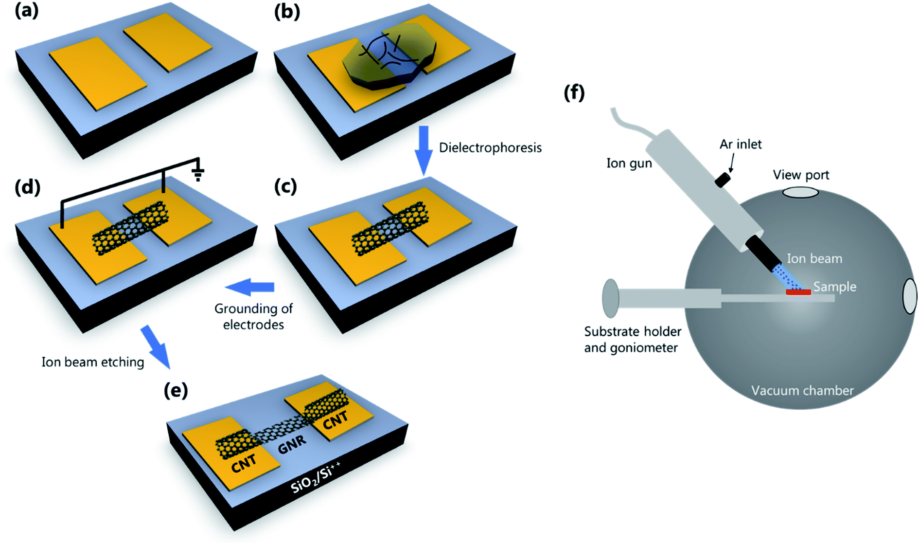 | ||
| Fig. 1 Steps involved in CNT alignment and ion beam processing. (a) Empty gold metal gap electrodes on a SiO2/Si substrate, (b) a drop of IPA containing CNTs is placed across the electrodes, (c) aligned CNTs by dielectrophoresis, (d) grounding of metal electrodes, (e) formation of the CNT–GNR–CNT junctions after ion beam exposure, and (f) the set-up for IBE. | ||
Ion beam etching
The device substrate containing aligned CNTs was loaded in a vacuum chamber having a goniometer with a substrate holder, an electrical feedthrough, and an Ar ion gun (Omicron FDG 150). The base vacuum created was 5 × 10⁻⁷ Torr. Ion gun parameters were tuned to produce a beam of 0.5 cm diameter. The electrical connections from gold electrodes were carefully taken out for grounding (Vground ≈ 0.01 V). For etching, the ion energy was tuned from 3 to 4 keV in a vacuum of 5 × 10⁻⁵ Torr with a beam current of 1–3 mA. After exposure, the sample was kept in a high vacuum for 30 min to cool down.Characterization
CNT and GNR formation was probed at various stages using a Nova NanoSEM 600 instrument (FEI Co., The Netherlands). Scanning probe microscopy was carried out on an Innova Bruker instrument with a 30 nm Si tip in tapping mode. Raman spectra were recorded by using a Horiba LABRAM HR Evolution with 633 nm. The image colour processing was performed on Mipar© software. Electrical measurements were acquired using a Keithley 4200 SCS in the ambient environment at room temperature.Results and discussion
Here, multi-walled carbon nanotubes (CNTs) are used due to their well-known metallic nature, long length and bendable properties. They were aligned across gold metal electrodes using dielectrophoresis (Fig. 1a–e).10 Multiple devices were fabricated with a single CNT and a few CNTs across metal electrodes. After alignment, the substrate was exposed to a 3–4 keV Ar ion beam under 5 × 10⁻⁵ Torr to etch the CNTs (Fig. 1f). It should be noted that the CNT ends are in contact with the thin metal while the middle portion is touching the insulating oxide. It is well known that during sputter etching there is charging of the material as well as the substrate due to the formation of charged species such as ions and electrons. Hence, if any bias or grounding is applied, it is possible to guide these charges, which may affect the etching. To date, insufficient attention has been paid to these kinds of effects in nanoscale materials like CNTs. Usually, ion beams etch CNTs everywhere along their length independent of whether they are lying on a metallic or insulating substrate (see ESI Fig. S1†). We observed that during ion exposure the etching of CNTs overlapping the metal region depends on whether the metal contacts are connected to the ground or not (see ESI Fig. S2†). If they are not grounded, then charged ions etch CNTs in equal proportion along their whole length. In other case, if metal electrodes are grounded, then the portion of the CNTs away from the metal contact which is touching the insulating background is etched. This is because positively charged Ar ions are neutralized on the metal region and get removed immediately through the ground, but they do get reflected from the insulating area and remove carbon atoms in the CNTs. Note that the metal gap is sufficiently long (7 μm) compared to the diameter of CNTs (120 ± 20 nm) and the Ar ion diameter so that the formation of this kind of gradient is feasible. We found neither formation or change in potential nor currents at the ground electrode during this neutralization process (on a time scale of seconds), which eliminates the possibility of crowding of positive or negative charges which may affect the etching rate. Thus, CNT–GNR–CNT dual junctions are obtained (vide infra). At shorter channel lengths in the sub-micron region, this effect will be feeble due to the highly conducting nature of CNTs. Hence, this method is more suitable for making such molecular junctions of extended dimensions.Structural analysis of GNR formation was carried out by scanning electron microscopy (SEM), atomic force microscopy (AFM) and Raman spectroscopy (Fig. 2). The etch time was varied from 0 s to 10 min. With an increase in exposure time, etched regions of the CNTs increase (Fig. 2a–c). In the false coloured SEM images the etched region appears bluish (similar to the substrate) and the reactive edges are brighter and yellowish. Surprisingly, the etching rate is found to be similar for both with and without metal electrode grounding (see ESI Fig. S2†). The observed etching yield of 1 atom/ion matches well with Ar ion usage for carbon films.8 The intermediate steps of etching are probed by SEM (see ESI Fig. S3†), which shows that after 3 min of exposure, there are formation of whiskers and opening of CNTs. With time, the opened side walls diminished and then there is a vertical etching of ribbons. For an etching time of 10 min, the minimum width and thickness are observed to be ∼80 nm and ∼0.8 nm, respectively (Fig. 2d). The formation of GNRs is further confirmed by Raman spectroscopy (Fig. 2e). The spectra show standard D, G, and 2D peaks for CNT and graphene.11 The intensity ratio of 2D to G indicates the presence of 2 or 3 layers of graphene.12 The ratio of the D to G peak area (A) for our GNRs is AD/AG ∼ 1–2, which is comparable to that of the GNRs obtained from CVD (∼1–5) and exfoliated (∼2–8) graphene etching with O2 plasma.13 Further, the crystallite size (La) is obtained from these Raman peaks using,
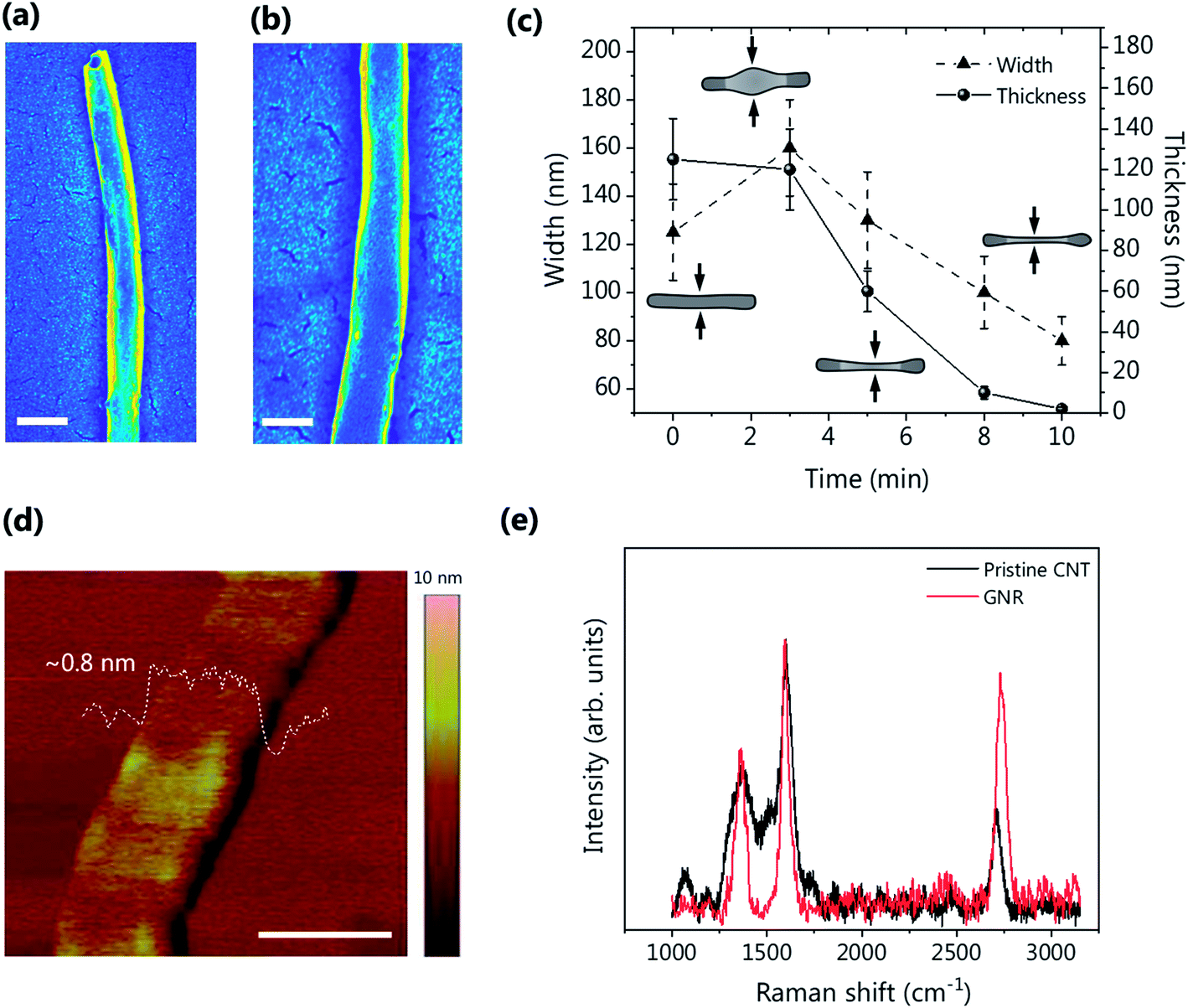 | ||
| Fig. 2 (a and b) False colour SEM images of CNTs after Ar ion exposure for 1 and 3 min, respectively. The etched regions of the CNTs are blue in colour which matches with the background. (c) Variation of CNT width and GNR thickness as a function of Ar ion exposure time. The arrows indicate the tentative positions where width is measured. The error bars correspond to measurements of several CNTs. (d) AFM image and (e) Raman spectra of GNRs are obtained for an ion exposure time of 10 min. Scale bars: (a) 200 nm, (b) 100 nm, and (d) 100 nm. | ||
To characterize the transport properties of the CNT–GNR–CNT seamless junction, field effect transistor (FET) measurements were performed in air at room temperature. For a device with a single pristine CNT (Fig. 3a), the output current–voltage (IV) characteristics (Fig. 3b) are linear, indicating the metallic nature of CNT with a resistance of 5.85 KΩ. After etching for 10 min with grounding the electrodes, the formed GNR IV curve showed 103 times reduction in current but maintained its linearity. From the transfer IV curves it is evident that, as expected, the pristine CNT does not show a change in current with the application of the gate voltage (Fig. 3c). For an etching time of 10 min, good current modulation is observed with ambipolar conduction. The current on/off ratio is noted to be 27 for VDS = 0.1 V. To date, diverse experimental values have been obtained for current on/off ratios in GNR FETs, which are quite different from the theoretical predictions.16–18 This is due to the variations in several experimental parameters such as contact resistance, interface contamination during fabrication, dielectrics used, measurement conditions, etc. Field effect mobility for hole and electron is obtained to be 350 and 130 cm2 V−1 s−1, respectively. These values are very good considering the large L/W ratio and the fact that the crystallite size is similar to the width.13
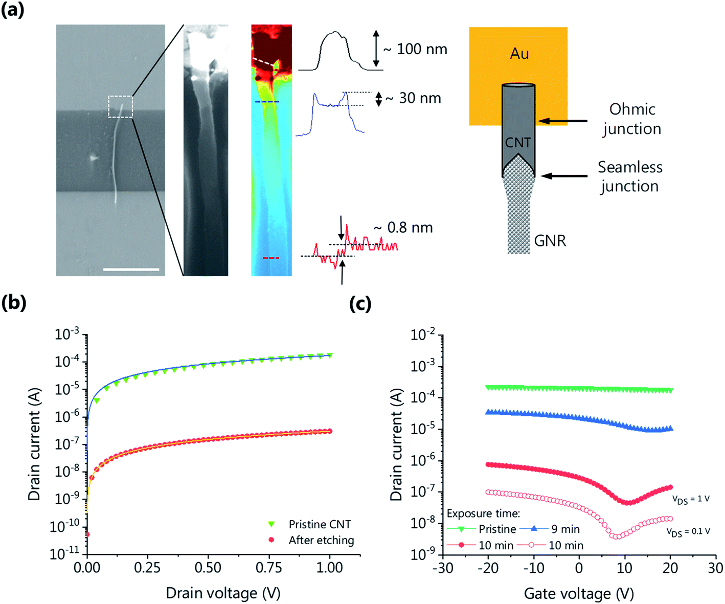 | ||
| Fig. 3 (a) The grey colour SEM images of a single CNT aligned across metal electrodes before (left) and after etching (right, zoom-in) when metal electrodes were grounded. The false colour image is obtained by software processing of the right side SEM image which indicates variation of thickness along the length of the CNT from the metal edge. The line profiles are obtained from the dotted lines. The schematic depicts the formation of ohmic and seamless junctions between the metal, CNT and GNR. (b) Current–voltage characteristics of CNT and CNT–GNR–CNT devices are shown on the semi-log scale with a linear fit. (c) Transistor transfer characteristics of CNT and GNR at different ion exposure times. | ||
Identification of a suitable inorganic metal contact for the GNRs is an important task. Metallic CNTs themselves could be the best choice, which can maintain similar bonding and form a seamless junction.3 This seamless junction has its own advantages for charge transport. We identified a unique way to fabricate it efficiently. In general, for IBE, grounding of active materials (target) has not been paid sufficient attention and its effects on the process outcome are largely unknown. It is important on the nano scale since formation of local charged or neutral zones may affect the shapes of materials. By using the simple concept of grounding and ion beam etching, we have successfully developed a process which produces a double seamless junctions of CNT–GNR–CNT. The fabricated device works as a FET with good charge carrier mobility over large distances. The Raman analysis of AD/AG and ID/IG showed that the distance between the defects is La ∼ 65 nm which is quite large and indicates that ion bombardment has not created large defects in the ribbon plane. Without grounding of electrodes, we observed uniform etching of CNTs to form GNRs even over metal overlapping regions (see ESI Fig. S2 and S4†). To enhance the understanding and working of this kind of device, we need additional experimental studies as well as theoretical analysis. Further, the nature of edges and their effect on transport can be investigated. The developed method has strong potential to obtain high throughput in fabricating these kinds of devices since dielectrophoresis of CNTs is possible at the industrial scale. As theoretically predicted by Santos et al.2 for a CNT–GNR–CNT junction, tubes act as completely transparent contacts and such systems are by themselves magnetoresistive devices with a large value of magnetoresistance. Hence, these seamless intramolecular junctions can act as efficient filters in valleytronics.19
Conclusions
In summary, we have shown experimentally that the formation of CNT–GNR–CNT seamless junctions is possible with good reproducibility for transistor applications. Multi-walled CNTs are used as the source material and etched with an Ar ion beam to form GNRs. During exposure to the ion beam, if electrodes are grounded, the positive ions sputter etch the CNTs away from the CNT–metal junction, and without grounding, etching occurs uniformly over the whole length. Thus, a 2 or 3 layers GNR transistor with high aspect ratio shows good performance at room temperature. This work will pave the way to test experimentally novel phenomena for quantum computers and various applications of CNT–GNR junctions.Conflicts of interest
There are no conflicts to declare.Acknowledgements
The authors thank Prof. G. U. Kulkarni for support and encouragement. We also thank Thripuranthaka M. Nagaleekar for technical assistance. The work is financially supported by DST-SERB Early Career Award SERB/2017/1562 and SRM IST.References
- D. Wei, L. Xie, K. K. Lee, Z. Hu, S. Tan, W. Chen, C. H. Sow, K. Chen, Y. Liu and A. T. S. Wee, Nat. Commun., 2013, 4, 1374 CrossRef PubMed.
- H. Santos, L. Chico and L. Brey, Phys. Rev. Lett., 2009, 103, 086801 CrossRef CAS PubMed.
- Y. Ouyang and J. Guo, Appl. Phys. Lett., 2010, 97, 263115 CrossRef.
- L. Leem, A. Srivastava, S. Li, B. Magyari-Kope, G. Iannaccone, J. S. Harris and G. Fiori, in 2010 International Electron Devices Meeting, IEEE, 2010, pp. 32.5.1–32.5.4 Search PubMed.
- W. Xu and T.-W. Lee, Mater. Horiz., 2016, 3, 186–207 RSC.
- L. Jiao, L. Zhang, X. Wang, G. Diankov and H. Dai, Nature, 2009, 458, 877–880 CrossRef CAS PubMed.
- L. Jiao, L. Zhang, L. Ding, J. Liu and H. Dai, Nano Res., 2010, 3, 387–394 CrossRef CAS.
- K. Karahashi, H. Li, K. Yamada, T. Ito, S. Numazawa, K. Machida, K. Ishikawa and S. Hamaguchi, Jpn. J. Appl. Phys., 2017, 56, 06HB09 CrossRef.
- R. Krupke, F. Hennrich, H. v. Löhneysen and M. M. Kappes, Science, 2003, 301, 344–347 CrossRef CAS PubMed.
- L. An, D. D. Cheam and C. R. Friedrich, J. Phys. Chem. C, 2009, 113, 37–39 CrossRef CAS.
- U. K. Parashar, S. Bhandari, R. K. Srivastava, D. Jariwala and A. Srivastava, Nanoscale, 2011, 3, 3876 RSC.
- A. A. Sagade, A. I. Aria, S. Edge, P. Melgari, B. Gieseking, B. C. Bayer, J. C. Meyer, D. Bird, P. Brewer and S. Hofmann, npj 2D Mater. Appl., 2017, 1, 35 CrossRef.
- A. Behnam, A. S. Lyons, M.-H. Bae, E. K. Chow, S. Islam, C. M. Neumann and E. Pop, Nano Lett., 2012, 12, 4424–4430 CrossRef CAS PubMed.
- L. G. Cançado, K. Takai, T. Enoki, M. Endo, Y. A. Kim, H. Mizusaki, A. Jorio, L. N. Coelho, R. Magalhães-Paniago and M. A. Pimenta, Appl. Phys. Lett., 2006, 88, 163106 CrossRef.
- A. Jorio, E. H. M. Ferreira, M. V. O. Moutinho, F. Stavale, C. A. Achete and R. B. Capaz, Phys. Status Solidi, 2010, 247, 2980–2982 CrossRef CAS.
- R. M. Jacobberger, B. Kiraly, M. Fortin-Deschenes, P. L. Levesque, K. M. McElhinny, G. J. Brady, R. Rojas Delgado, S. Singha Roy, A. Mannix, M. G. Lagally, P. G. Evans, P. Desjardins, R. Martel, M. C. Hersam, N. P. Guisinger and M. S. Arnold, Nat. Commun., 2015, 6, 8006 CrossRef CAS PubMed.
- W. J. Yu and X. Duan, Sci. Rep., 2013, 3, 1248 CrossRef PubMed.
- U. Zschieschang, H. Klauk, I. B. Müeller, A. J. Strudwick, T. Hintermann, M. G. Schwab, A. Narita, X. Feng, K. Müellen and R. T. Weitz, Adv. Electron. Mater., 2015, 1, 1400010 CrossRef.
- A. Rycerz, J. Tworzydło and C. W. J. Beenakker, Nat. Phys., 2007, 3, 172–175 Search PubMed.
Footnote |
| † Electronic supplementary information (ESI) available. See DOI: 10.1039/c9na00797k |
| This journal is © The Royal Society of Chemistry 2020 |