
 Open Access Article
 This Open Access Article is licensed under a Creative Commons Attribution-Non Commercial 3.0 Unported Licence
Design of a dual-band terahertz metamaterial absorber using two identical square patches for sensing application
Ben-Xin
Wang
 *,
Yuanhao
He
,
Pengcheng
Lou
and
Wenhui
Xing
*,
Yuanhao
He
,
Pengcheng
Lou
and
Wenhui
Xing
School of Science, Jiangnan University, Wuxi, 214122, China. E-mail: wangbenxin@jiangnan.edu.cn
First published on 3rd January 2020
Abstract
A dual-band terahertz metamaterial absorber composed of two identical square metallic patches and an insulating medium layer on top of a continuous metallic ground is demonstrated. Two resonance peaks (labeled A and B) with near 100% absorbance are obtained, of which peak A derived from the localized resonance of the two square patches has a line-width of 0.2571 THz and quality factor of 6.9156, while peak B which resulted from the hybrid coupling of the localized resonance of the two square patches and surface lattice resonance of the device has a very narrow line-width of 0.0083 THz and large quality factor of 296.2771. Narrow line-width and large quality factor have important prospects in sensing application. Based on this, the sensing performance of the device is explored; it is revealed that peak B exhibits highly sensitive sensing ability (including a sensing sensitivity of 1.9010 THz per RIU and figure of merit of 229.04) in terms of the surrounding index. In addition, the influence of structural parameters on the absorption performance is discussed to further verify the formation mechanism of these two absorption peaks.
Introduction
Metamaterials using periodic or aperiodic artificial sub-wavelength or deep-sub-wavelength structural designs have attracted the interest of many researchers due to their novel and peculiar physical properties (such as negative refraction, perfect lensing and cloaking) that are extremely difficult to realize in nature.1 The main reason for these novel physical properties is the lattice design of the metamaterials rather than the materials that make them. As a result, instead of only focusing on novel physical properties, researchers are gradually turning to how to use the resonance characteristics of metamaterials to design some resonant devices with specific functions. This is why in recent years we have witnessed a wide range of reports and presentations based on metamaterial resonant devices,2–5 including filters, modulators, sensors, polarization conversion devices, absorbers, etc. Among these resonant devices, metamaterial absorbers have attracted extensive attention because of their excellent performance and wide application potential.6–8The first type of metamaterial absorber made up of three layers including a metallic electric-ring resonator, an ultra-thin FR4 dielectric layer and a metallic cut-wire was demonstrated in 2008.6 The metamaterial could achieve near-perfect absorption at 11.25 GHz. More importantly, the thickness of the FR4 dielectric material is only 1/35 of the resonant wavelength.6 Such an ultra-thin dielectric thickness not only ensures the light weight of the device, but can also be easily constructed. In view of these excellent features (near-perfect absorption, ultra-thin dielectric layer thickness, light weight etc.), the metamaterial absorber can have great application prospects in terms of selective thermal emitters, spectral imaging, sensing and detection etc.7,8 However, limited to the single frequency point absorption and microwave frequency domain,6 the presented metamaterial absorber has some limitations in applications.
To expand the application prospects and field of metamaterial absorbers, the number of absorption frequency points (or absorption peaks) and working frequency bands of metamaterial absorbers need to be broadened. The working frequency of the metamaterial absorber can be easily controlled by appropriately scaling the structure size. For example, reducing the structure size of the first type of metamaterial absorber can cause the working frequency of the device to be located at the terahertz frequency range of the high frequency band.9 Similar scaling of the other structures can also control the working frequency of the metamaterial absorbers.10,11 However, it is difficult to control the number of absorption frequency points (or absorption peaks) by only scaling the metamaterial structure.
The most effective way to increase the number of absorption peaks is to introduce several different-sized metallic resonators into the lattice structure. Resonators with different sizes possess the ability to produce absorption peaks of different specific frequencies, and their superposition effect will produce perfect absorption in multiple frequency bands.12–40 Based on this strategy, there are usually two ways of structural design to achieve the perfect absorption of the incident beam in multiple frequency points. The first one is to place these sub-resonators in a coplanar manner on a large-scale lattice structure, and the other one is to vertically stack these metallic elements to form a thick lattice structure. Based on the two methods, metamaterial absorbers with multiple frequency bands (i.e., multiple-band absorbers) using various structures (or elements) have been widely studied and presented.12–39
Among these multiple-band absorption devices, dual-band absorbers are the simplest and most frequently mentioned multiple-band absorption devices, and therefore they have been widely investigated and reported. For example, coplanar structural design methods consisting of multiple sub-resonators were given to show two distinct absorption peaks in the specific resonance frequency region.18–26 Dual-band metamaterial absorbers were also demonstrated using the stacked structural design methods.27–34 Other structural designs were also suggested to achieve the dual-band absorption performance, including cuboid ferrite particle,35 circular sector resonator,36 graphene–SiC hybrid system,37 cylinder MoS2-dielectric array,38 and asymmetric double-split ring resonators.39
Although various kinds of structures have been proposed to achieve dual-band absorption, there are still many similar shortcomings in these designs, which limit their practical application to a certain extent. For example, their surface structures are relatively complex, which will increase the design complexity and manufacturing process of the device, consume too much structure optimization time, and reduce the absorption strength of the device due to the strong interaction of the sub-units or sub-sections.18–39 More importantly, the line-width of these absorption devices is usually large, which is about one tenth to one fifth of the absorption frequency.12–39 The absorption peak with such a large line-width is not conducive to the practical applications of sensing and detection. It is a well-known fact that the sensing performance based on metamaterial absorbers has great advantages over the traditional metallic-dielectric-based metamaterial structures.40–42 However, to obtain better sensing performance, it is necessary to significantly narrow the resonance line-width of the existing absorption devices because this is a very important index in evaluating the sensor application potential. The above results show that it is quite reasonable to design dual-band metamaterial absorbers with a simple surface structure and ultra-narrow resonance line-width suitable for sensing applications. However, metamaterial absorbers with these specific functions are rarely reported.
In this paper, a new type of dual-band metamaterial absorber operating at terahertz frequency is presented. Different from the complex surface structures of the existing dual-band metamaterial absorbers, the device suggested here is designed by combining the simple surface structures of two identical square metallic patches, which are placed on an ultra-thin dielectric slab and a continuous metallic board. Two discrete absorption peaks with near 100% absorbance are obtained. The first absorption peak mainly comes from the localized resonance response of square metallic patches, while the second one is from the superposition effect of the localized resonance response of the square patches and the surface lattice resonance of the device, and therefore this mode has a narrower absorption line-width and higher quality factor than the first absorption peak. Based on this, the sensing performance of the absorption device is discussed. The second absorption peak is very sensitive to the change in the refractive index of the surroundings. A sensing sensitivity of 1.9010 THz per RIU and figure of merit of up to 229.04 can be obtained, which are significantly higher than the sensing performance of many existing metamaterial absorbers and other reported technologies operating at terahertz frequency, see below, Table 1.
Structural design and model
Fig. 1(a) and (b) show the basic cell of the designed dual-band terahertz metamaterial absorber. As revealed in Fig. 1(a), it is formed by two identical square metallic patches with a thickness of 0.4 μm and an ultra-thin insulator dielectric layer of t = 4.1 μm on top of a continuous metallic ground. The detailed parameters of the dual-band absorber are shown in the top-view of Fig. 1(b). The two square patches have the same length and width of l = w = 44 μm, and the gap between them is g = 6 μm. The two patches are placed on a dielectric-metallic-based layer with a period of Px = 120 μm and Py = 70 μm. The middle insulator layer is a kind of dielectric material having the dielectric constant of 3(1 + i0.06). The top metallic pattern structures and the bottom metallic board are both made of Au having a conductivity of 4.09 × 10⁷ S m−1. A finite-difference time-domain based algorithm is utilized to obtain accurate preset results. In the specific calculation process, a plane electromagnetic beam polarized along the x axis is employed to irradiate the designed device. Periodic boundary conditions used to demonstrate the periodic arrangement of the absorption device are applied to the x and y axes, while the perfectly matched layers for absorbing unnecessary scattered light are applied to the z axis.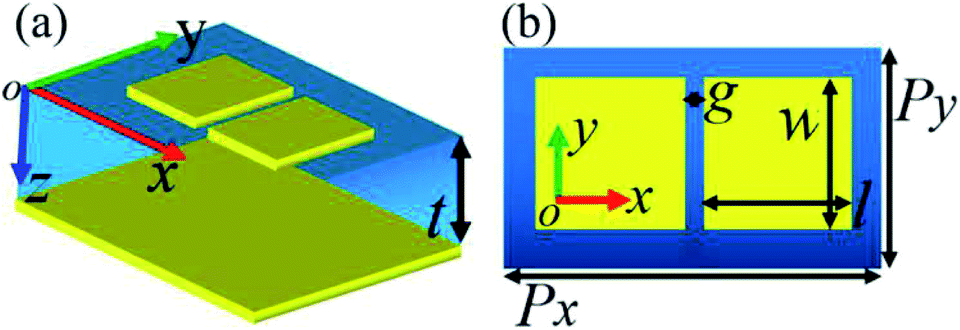 | ||
| Fig. 1 (a) Three-dimensional diagram of the basic cell of the dual-band terahertz metamaterial absorber; (b) plane (top view) diagram of the basic cell of the dual-band terahertz metamaterial absorber. | ||
Results and discussion
The absorption of the device can be written as A = 1 − T − R, where A, T, and R are the coefficients of absorption, transmission, and reflection, respectively. T is equal to zero because the used metallic board can completely block the transmission of the incident beam. R can also be made zero by selecting an appropriate thickness of the dielectric layer so that the impedance of the metamaterial matches that of the air. Simultaneous zero transmission and reflection can ensure that the resonant device shows near-unity absorption. Fig. 2 shows the absorption spectrum under the optimal structural parameters. As revealed, two discrete resonance peaks (marked A and B) with nearly 100% perfect absorption are found. Peak A with resonance frequency at 1.7780 THz has an absorption line-width of 0.2571 THz, and its line-width is about one seventh of the resonance frequency, which is in line with the spectral characteristics of the existing metamaterial absorbers, which shows that peak A is a perfect absorption peak in the traditional sense, and the following theoretical explanations confirm this. It should be noted that the so-called absorption line-width refers to the full width at half maximum; in this case it refers to the span with 50% absorption (see the black dashed line in Fig. 2). Furthermore, according to the definition of quality factor (Q),40–42 the Q value of peak A is 6.9156.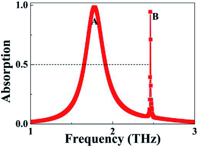 | ||
| Fig. 2 Absorption response of the dual-band metamaterial absorber. | ||
Different from the spectral characteristics of peak A, absorption peak B with resonance frequency at 2.4591 THz has a very narrow line-width of 0.0083 THz, and its corresponding Q value is as high as 296.2771. Compared with peak A, peak B not only has a narrower line-width, but also a higher quality factor. The absorption line-width and Q value of peak B are respectively about one thirtieth and 42.84 times that of peak A. The existing metamaterial absorbers6–35 do not possess the two features (ultra-narrow absorption line-width and ultra-high Q value) and the following results show that peak B is mainly derived from the surface lattice resonance of the basic cell. So the resonance mode has a narrow absorption line-width and large Q value. As we all know, a narrow line-width and a large Q value are the basic and necessary conditions for the sensitive sensing performance of resonant devices. The results given in Fig. 6 confirm this; it is revealed that the sensing sensitivity and figure of merit of peak B are respectively 1.9010 THz per RIU and 229.04, which are significantly larger than that of the sensing ability of many existing metamaterial absorption devices and other technologies operating at terahertz frequency, see below, Table 1.
Near-field distributions of the two absorption peaks (A and B) are given to reveal their formation mechanisms. Fig. 3(a), (b) and (c) are respectively the amplitude of the electric field (|E|), z component of the electric field (real Ez), and the amplitude of the magnetic field (|H|) of peak A at 1.7780 THz. The electric field (|E|), electric field (real Ez), and magnetic field (|H|) of peak B at 2.4591 THz are presented in Fig. 3(d), (e) and (f), respectively. For resonance peak A at 1.7780 THz, we found that its near-field patterns in Fig. 3(a) and (b) are both symmetrically distributed on the edges of the two identical square patches, which indicate that peak A should be derived from the localized resonance response of the two square patches. More specifically, for the electric fields in Fig. 3(a), it can be observed that they are mainly localized at the edges of two identical square patches, while it is difficult to see the field distributions in other areas, including the gap between the two patches and the non-metallic resonance areas. The z component of electric fields (real Ez) in Fig. 3(b) has similar distribution characteristics in that it is mostly concentrated at the sides of the square patches and almost no field patterns are gathered in the non-metallic areas. These electric fields (|E|, real Ez) show that the dipole resonance will be generated when the square patches on the left and right interact with the incident beam. The dipole resonance on the square patches can interact with the bottom metallic board, and generate an anti-parallel current, so that the induced magnetic field could be concentrated at the insulating dielectric layer under the metallic array. The magnetic fields in Fig. 3(c) indeed show such characteristics in that strong field aggregation can be found in the insulator dielectric layer under the square patches on the left and right.
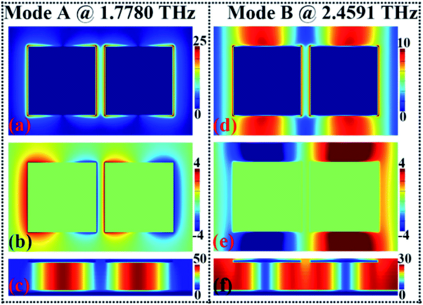 | ||
| Fig. 3 Near-field (amplitude of the electric field (|E|) in (a), z component of the electric field (real Ez) in (b), amplitude of the magnetic field (|H|) in (c)) distributions of resonance peak A at 1.7880 THz; near-field (amplitude of the electric field (|E|) in (d), z component of the electric field (real Ez) in (e), amplitude of the magnetic field (|H|) in (f)) distributions of resonance peak B at 2.4591 THz. | ||
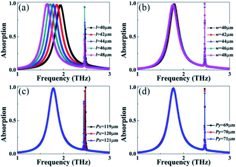
Different from the field distribution characteristics of resonance peak A in Fig. 3(a) and (b), the field patterns of peak B in Fig. 3(d) and (e) not only focus on the edges of the square patches, but also on the non-metallic areas, which reveals that peak B should be due to the combination effect of the localized resonance response of the metallic array and the surface lattice resonance of the whole metamaterial. Of course, the magnetic field patterns in Fig. 3(f) also give further evidence. It is observed that strong magnetic field gathering can be found in the insulating dielectric layer under the metallic array and the non-metallic array. Because the formation mechanism of peak B mainly contributes to the localized resonance mode of the metallic array and the surface lattice resonance of the whole metamaterial, the changes in the metallic array size and the lattice period could strongly affect the resonance frequency and even the absorption intensity of peak B. However, this is not the case. The results given below in Fig. 4 and 5 show that the resonance performance of peak B is mainly controlled by the lattice period P, while the size changes of the metallic array hardly affect its resonance frequency. This is mainly due to the difference of electric field distributions between the metallic array and the non-metallic areas. As observed in Fig. 3(d) and (e), the proportion of electric field patterns in the non-metallic areas is much larger than that of the edges of metallic sections or the field distributions in the non-metallic areas are much stronger than that of the edges of the metallic array.
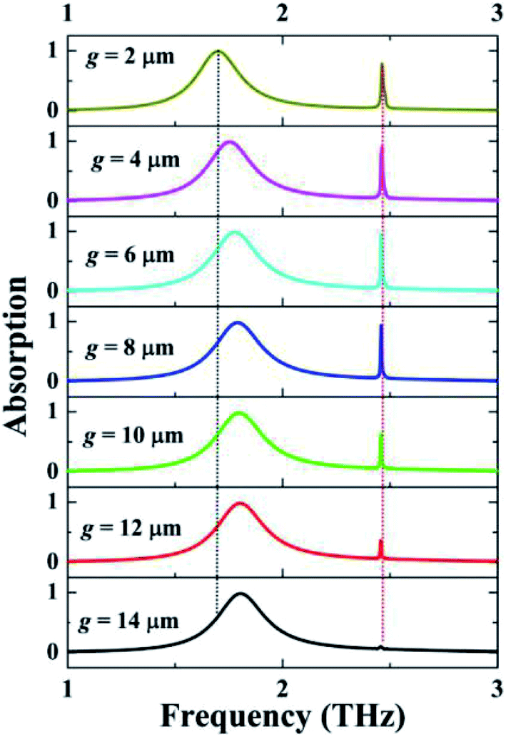 | ||
| Fig. 4 Dependence of the absorption spectrum on the changes of the gap (g) between the two identical square patches. | ||
 | ||
| Fig. 5 Dependence of the absorption spectrum on the changes of length (l) in (a); width (w) in (b); lattice period (Px) in (c); and lattice period (Py) in (d). | ||
The variation of structural parameters is discussed to further evaluate the resonance performance of the dual-band absorption device, and the dependence of the absorption spectrum on the structure size can further verify the formation mechanism of the two absorption peaks (A and B) and the correctness of the theoretical explanations demonstrated in the above two paragraphs. We first study the effect of the gap (g) between the two square patches on the absorption performance. It should be noted that we keep the sum of the original length (l = 44 μm) of the two patches and their original gap (g = 6 μm) as a fixed value (FV), and the FV = l + l + g = 44 + 44 + 6 = 94 μm. In view of this, the change in the gap (g) can indirectly adjust the length (l) of the square patches, namely, the larger the gap (g), the smaller the patch length (l). It is a known fact that the frequency of the localized resonance response of the metallic array is inversely proportional to its length, that is, a larger length (l) corresponds to a smaller frequency. It can be predicted that the frequency of the resonance peak A will gradually increase with the increase of the gap (g) or the decrease of length (l). As revealed in Fig. 4, the frequency of resonance peak A indeed shows an increasing trend when the gap (g) increases, which is consistent with the theoretical prediction.
Different from the change in the resonance peak A, the frequency of the resonance peak B is almost unchanged; the answer may be hidden in its field distributions. As observed in Fig. 3(d) and (e), negligible electric field patterns are found in the gap (g) of the square patches, and therefore the change in the gap (g) cannot regulate the resonance frequency of this mode. However, the variation of the gap (g) could change the impedance of the metamaterial, especially at the gap, so the absorption intensity of the resonance peak B is regulated. As a typical example, when the gap (g) is 14 μm, the absorption intensity of peak B can be almost completely suppressed, and thus the designed device has only a single absorption peak, which becomes the single-band metamaterial absorber. Other structural parameters, such as patch length (l), patch width (w), and lattice period (Px and Py), are further investigated to analyze the effect on the resonance performance. As presented in Fig. 5, the size variations of the metallic array can hardly affect the resonance frequency of the absorption peak B, while an extremely slight change of the lattice period can obviously affect the resonance frequency of the absorption peak B. These results indicate that the first absorption peak A is primarily due to the localized resonance response of the metallic array, and therefore its frequency is mostly controlled by the structural parameters of the metallic array (i.e., the square patches), and has nothing to do with the change of the lattice period. However, the frequency of the second absorption peak B is different from that of absorption peak A, the change of its frequency is mainly controlled by the lattice period, while its frequency hardly changes when the parameters of the metallic array are varied. It is confirmed that the absorption peak B is mainly derived from the surface lattice resonance of the whole metamaterial, which is due to the fact that the frequency of the surface lattice resonance is strongly dependent on the lattice period change and slightly subject to the parameter changes of the metallic array itself.43–45
Since the second resonance peak B has a narrow absorption line-width and large quality factor, the resonance frequency of this mode will strongly depend on the variation of the refractive index of the surrounding. For verification, the dependence of the absorption spectrum on the refractive index (n) change of the surrounding is presented in Fig. 6. The variation range of the refractive index studied here is n = 1.00–1.10, which increases with an interval of 0.02. As found in Fig. 6(a), the resonance frequency of the first absorption peak A is almost unchanged with the increase of the refractive index (n), while the frequency of the second absorption peak B shows a strong dependence on the refractive index (n). The higher the refractive index (n), the lower the resonance frequency. The relationship between the resonance frequency of the second absorption peak B and the refractive index (n) is shown in Fig. 6(b). It is revealed that an approximate inverse proportion relationship is obtained.
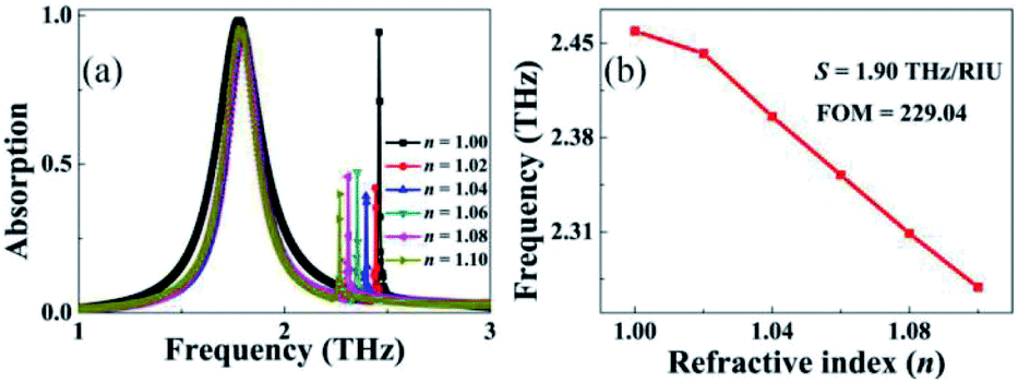 | ||
| Fig. 6 (a) Dependence of the absorption spectrum on the changes of the refractive index (n) of the surrounding; (b) relationship between the resonance frequency and refractive index. | ||
To evaluate the response of the absorption device to the refractive index (n) change of the surrounding, sensitivity (S) is usually calculated. S is defined as: S = Δf/Δn, where Δf and Δn are respectively the changes in the frequency and refractive index.40–42 Combined with the calculation data in Fig. 6, the S of the second absorption peak is 1.90 THz per RIU, this is a pretty good value. In fact, in addition to S, the figure of merit (FOM) is a more important index, which can be used to directly compare the sensing performances of different kinds of sensing devices. For its definition, please refer to ref. 40–42. The larger the FOM, the better the sensing performance. Using the data involved in the FOM definition and formula, the FOM of the second absorption peak B was found to be as high as 229.04, which is about two orders of magnitude higher than that of the metamaterial absorbers based on the localized resonance response of the metallic array(s).40–42 More importantly, the absorption device designed here with a large S and particularly a high value of FOM has better sensing performance than the existing reported technology operating at terahertz frequency, see Table 1.40–42,46–55
Conclusions
A fairly simple design of a dual-band terahertz metamaterial absorption device formed by two identical square patches and a continuous metallic mirror separated by an insulator medium is reported. Two resonance peaks with near perfect absorbance are realized, their physical mechanisms are discussed with the aid of their near-field patterns. The first absorption peak which resulted from the localized resonance response of the top metallic array has an absorption line-width of 0.2571 THz and a quality factor of 6.9156, while the second absorption peak, which mainly comes from the surface lattice resonance of the whole metamaterial structure, has an extremely narrow line-width of 0.0083 THz and ultra-high quality factor of 296.28. Because of the different formation mechanisms, the two absorption peaks have different changing tendencies to the variations of the structural parameters. Considering the characteristics (ultra-narrow absorption line-width, ultra-high quality factor) of the second absorption peak, the sensing performance of the suggested absorption device is discussed. It is revealed that the second absorption peak is rather sensitive to a minor change of the refractive index of the surrounding and exhibits highly sensitive sensing ability (including a sensing sensitivity of 1.9010 THz per RIU and figure of merit of 229.04).Conflicts of interest
There are no conflicts of interest to declare.Acknowledgements
This research was funded by the National Natural Science Foundation of China grant number 11647143, Natural Science Foundation of Jiangsu grant number BK20160189, China Postdoctoral Science Foundation grant number 2019M651692, Jiangsu Postdoctoral Science Foundation grant number 2018K113C, Fundamental Research Funds for Central Universities grant number JUSRP51721B.References
- D. Schurig, J. J. Mock, B. J. Justice, S. A. Cummer, J. B. Pendry, A. F. Starr and D. R. Smith, Metamaterial electromagnetic cloak at microwave frequencies, Science, 2006, 314, 977 CrossRef CAS PubMed.
- A. Ghobadi, H. Hajian, M. Gokbayrak, B. Butun and E. Ozbay, Bismuth-based metamaterials: from narrowband reflective color filter to extremely broadband near perfect absorber, Nanophotonics, 2019, 8, 823 CAS.
- A. Keshavarz and A. Zakery, A novel terahertz semiconductor metamaterial for slow light device and dual-band modulator applications, Plasmonics, 2018, 13, 459 CrossRef CAS.
- Y. Jiang, Z. Liu, N. Matsuhisa, D. Qi, W. R. Leow, H. Yang, J. Yu, G. Chen, Y. Liu, C. Wan, Z. Liu and X. Chen, Auxetic mechanical metamaterials to enhance sensitivity of stretchable strain sensors, Adv. Mater., 2018, 30, 1706589 CrossRef PubMed.
- J. Zi, Q. Xu, Q. Wang, C. Tian, Y. Li, X. Zhang, J. Han and W. Zhang, Antireflection-assisted all-dielectric terahertz metamaterial polarization converter, Appl. Phys. Lett., 2018, 113, 101104 CrossRef.
- N. I. Landy, S. Sajuyigbe, J. J. Mock, D. R. Smith and W. J. Padilla, Perfect metamaterial absorber, Phys. Rev. Lett., 2008, 100, 207402 CrossRef CAS PubMed.
- C. M. Watts, X. Liu and W. J. Padilla, Metamaterial electromagnetic wave absorbers, Adv. Mater., 2012, 24, OP98 CAS.
- Y. Cui, Y. He, Y. Jin, F. Ding, L. Yang, Y. Ye, S. Zhong, Y. Lin and S. He, Plasmonic and metamaterial structures as electromagnetic absorbers, Laser Photonics Rev., 2014, 8, 495 CrossRef CAS.
- H. Tao, N. I. Landy, C. M. Bingham, X. Zhang, R. D. Averitt and W. J. Padilla, A metamaterial absorber for the terahertz regime: Design, fabrication and characterization, Opt. Express, 2008, 16, 7181 CrossRef PubMed.
- X. Liu, T. Starr, A. F. Starr and W. J. Padilla, Infrared spatial and frequency selective metamaterial with near-unity absorbance, Phys. Rev. Lett., 2010, 104, 207403 CrossRef PubMed.
- D. Y. Shchegolkov, A. K. Azad, J. F. Ohara and E. I. Simakov, Perfect subwavelength fishnetlike metamaterial-based film terahertz absorbers, Phys. Rev. B: Condens. Matter Mater. Phys., 2010, 82, 205117 CrossRef.
- M. D. Astorino, F. Frezza and N. Tedeschi, Ultra-thin narrow-band, complementary narrow-band, and dual-band metamaterial absorbers for applications in the THz regime, J. Appl. Phys., 2017, 121, 063103 CrossRef.
- S. Liu, J. Zhuge, S. Ma, H. Chen, D. Bao, Q. He, L. Zhou and T. J. Cui, A bi-layered quad-band metamaterial absorber at terahertz frequencies, J. Appl. Phys., 2015, 118, 245304 CrossRef.
- Q. Mao, C. Feng and Y. Yang, Design of tunable multi-band metamaterial perfect absorbers based on magnetic polaritons, Plasmonics, 2019, 14, 389 CrossRef CAS.
- G. Kajtar, M. Kafesaki, E. N. Economou and C. M. Soukoulis, Theoretical model of homogeneous metal-insulator-metal perfect multi-band absorbers for the visible spectrum, J. Phys. D: Appl. Phys., 2016, 49, 055104 CrossRef.
- Y. He, Q. Wu and S. Yan, Multi-band terahertz absorber at 0.1-1 THz frequency based on ultra-thin metamaterial, Plasmonics, 2019, 14, 1303–1310 CrossRef CAS.
- J. Wu, F. Zhang, Q. Li, J. Chen, Q. Feng and L. Wu, Infrared five-band polarization insensitive absorber with high absorptivity based on single complex resonator, Opt. Commun., 2020, 456, 124575 CrossRef CAS.
- Y. Ma, Q. Chen, J. Grant, S. C. Saha, A. Khalid and D. R. D. Cumming, A terahertz polarization insensitive dual band metamaterial absorber, Opt. Lett., 2011, 36, 945 CrossRef PubMed.
- H. Tao, C. M. Bingham, D. Pilon, K. Fan, A. C. Strikwerda, D. Shrekenhamer, W. J. Padilla, X. Zhang and R. D. Averitt, A dual band terahertz metamaterial absorber, J. Phys. D: Appl. Phys., 2010, 43, 225102 CrossRef.
- H. Li, L. H. Yuan, B. Zhou, X. P. Shen, Q. Cheng and T. J. Cui, Ultrathin multiband gigahertz metamaterial absorbers, J. Appl. Phys., 2011, 110, 014909 CrossRef.
- Z. H. Jiang, S. Yun, F. Toor, D. H. Werner and T. S. Mayer, Conformal dual-band near-perfectly absorbing mid-infrared metamaterial coating, ACS Nano, 2011, 5, 4641 CrossRef CAS PubMed.
- G. Yao, F. Ling, J. Yue, C. Luo, J. Ji and J. Yao, Dual-band tunable perfect metamaterial absorber in the THz range, Opt. Express, 2016, 24, 1518 CrossRef CAS PubMed.
- Y. Bai, L. Zhao, D. Ju, Y. Jiang and L. Liu, Wide-angle, polarization-independent and dual-band infrared perfect absorber based on L-shaped metamaterial, Opt. Express, 2015, 23, 8670 CrossRef CAS PubMed.
- B. Zhang, J. Hendrickson and J. Guo, Multispectral near-perfect metamaterial absorbers using spatially multiplexed plasmon resonance metal square structures, J. Opt. Soc. Am. B, 2013, 30, 656 CrossRef CAS.
- J. Zhang, J. Tian and L. Li, A dual-band tunable metamaterial near-unity absorber composed of periodic cross and disk graphene arrays, IEEE Photonics J., 2018, 10, 4800512 Search PubMed.
- J. Song, L. Wang, M. Li and J. Dong, A dual-band metamaterial absorber with adjacent absorption peaks, J. Phys. D: Appl. Phys., 2018, 51, 385105 CrossRef.
- S. Bhattacharyya, S. Ghosh, D. Chaurasiya and K. V. Srivastava, Bandwidth-enhanced dual-band dual-layer polarization-independent ultra-thin metamaterial absorber, Appl. Phys. A, 2015, 118, 207 CrossRef CAS.
- Z. Su, J. Yin and X. Zhao, Terahertz dual-band metamaterial absorber based on graphene/MgF2 multilayer structures, Opt. Express, 2015, 23, 1679 CrossRef CAS PubMed.
- N. Zhang, P. Zhou, D. Cheng, X. Weng, J. Xie and L. Deng, Dual-band absorption of mid-infrared metamaterial absorber based on distinct dielectric spacing layers, Opt. Lett., 2013, 38, 1125 CrossRef CAS PubMed.
- B. X. Wang, C. Tang, Q. Niu, Y. He and T. Chen, Design of narrow discrete distances of dual-/triple-band terahertz metamaterial absorbers, Nanoscale Res. Lett., 2019, 14, 64 CrossRef PubMed.
- R. Xing and S. Jian, A dual-band THz absorber based on graphene sheet and ribbons, Opt. Laser Technol., 2018, 100, 129 CrossRef CAS.
- M. D. Astorino, F. Frezza and N. Tedeschi, Ultra-thin narrow-band, complementary narrow-band, and dual-band metamaterial absorbers for applications in the THz regime, J. Appl. Phys., 2017, 121, 063103 CrossRef.
- G. Dayal and S. A. Ramakrishna, Design of multi-band metamaterial perfect absorbers with stacked metal-dielectric disks, J. Opt., 2013, 15, 055106 CrossRef.
- B. X. Wang, G. Z. Wang, X. Zhai and L. L. Wang, Polarization tunable terahertz metamaterial absorber, IEEE Photonics J., 2015, 7, 4600507 Search PubMed.
- W. Wang, J. Wang, M. Yan, J. Wang, H. Ma, M. Feng and S. Qu, Dual band tunable metamaterial absorber based on cuboid ferrite particles, J. Phys. D: Appl. Phys., 2018, 51, 315001 CrossRef.
- H. Luo and Y. Z. Cheng, Ultra-thin dual-band polarization-insensitive and wide-angle perfect metamaterial absorber based on single circular sector resonator structure, J. Electron. Mater., 2018, 47, 323 CrossRef CAS.
- Y. M. Qing, H. F. Ma, S. Yu and T. J. Cui, Tunable dual-band perfect metamaterial absorber based on a graphene-SiC hybrid system by multiple resonance modes, J. Phys. D: Appl. Phys., 2019, 52, 015104 CrossRef.
- C. Qiu, J. Wu, R. Zhu, L. Shen and B. Zheng, Dual-band near-perfect metamaterial absorber based on cylinder MoS2-dielectric arrays for sensors, Opt. Commun., 2019, 451, 226 CrossRef CAS.
- T. Lu, D. Zhang, P. Qiu, J. Lian, M. Jing, B. Yu and J. Wen, Ultrathin terahertz dual-band perfect metamaterial absorber using asymmetric double-split rings resonator, Symmetry, 2018, 10, 293 CrossRef.
- L. Cong, S. Tan, R. Yahiaoui, F. Yan, W. Zhang and R. Singh, Experimental demonstration of ultrasensitive sensing with terahertz metamaterial absorbers: A comparison with the metasurfaces, Appl. Phys. Lett., 2015, 106, 031107 CrossRef.
- R. Yahiaoui, S. Tan, L. Cong, R. Singh, F. Yan and W. Zhang, Multispectral terahertz sensing with highly flexible ultrathin metamaterial absorber, J. Appl. Phys., 2015, 118, 083103 CrossRef.
- X. Hu, G. Xu, L. Wen, H. Wang, Y. Zhao, Y. Zhang, D. R. S. Cumming and Q. Chen, Metamaterial absorber integrated microfluidic terahertz sensors, Laser Photonics Rev., 2016, 10, 962 CrossRef CAS.
- Z. Li, S. Butun and K. Aydin, Ultranarrow band absorbers based on surface lattice resonances in nanostructured metal surfaces, ACS Nano, 2014, 8, 8242 CrossRef CAS PubMed.
- V. G. Kravets, A. V. Kabashin, W. L. Barnes and A. N. Grigorenko, Plasmonic surface lattice resonances: A review of properties and applications, Chem. Rev., 2018, 118, 5912 CrossRef CAS PubMed.
- M. Manjappa, Y. K. Srivastava and R. Singh, Lattice-induced transparency in planar metamaterials, Phys. Rev. B, 2016, 94, 161103 CrossRef.
- Y. Li, X. Chen, F. Hu, D. Li, H. Teng, Q. Rong, W. Zhang, J. Han and H. Liang, Four resonators based high sensitive terahertz metamaterial biosensor used for measuring concentration of protein, J. Phys. D: Appl. Phys., 2019, 52, 095105 CrossRef.
- J. A. Burrow, R. Yahiaoui, W. Sims, Z. Chase, V. Tran, A. Saramgan, J. Mathews, W. S. Rockward, I. Agha and T. A. Searles, Influence of symmetry breaking on Fano-like resonances in high figure of merit planar terahertz metafilms, https://arxiv.org/pdf/181202063.pdf Search PubMed.
- M. Islam, S. J. M. Rao, G. Kumar, B. P. Pal and D. R. Chowdhury, Role of resonance modes on terahertz metamaterials based thin film sensors, Sci. Rep., 2017, 7, 7355 CrossRef PubMed.
- F. Shen, J. Qin and Z. Han, Planar antenna array as a highly sensitive terahertz sensor, Appl. Opt., 2019, 58, 540 CrossRef CAS PubMed.
- I. AI-Naib, Thin-film sensing via fano resonance excitation in symmetric terahertz metamaterials, J. Infrared, Millimeter, Terahertz Waves, 2018, 39, 1 CrossRef.
- A. S. Saadeldin, M. F. O. Hameed, E. M. A. Elkaramany and S. S. A. Obayya, Highly sensitive terahertz metamaterial sensor, IEEE Sens. J., 2019, 19, 7993 Search PubMed.
- K. Meng, S. J. Park, A. D. Nurnett, T. Gill, C. D. Wood, M. Rosamond, L. H. Li, L. Chen, D. R. Bacon, J. R. Freeman, P. Dean, Y. H. Ahn, E. H. Linfield, A. G. Davies and J. E. Cunningham, Increasing the sensitivity of terahertz split ring resonator metamaterials for dielectric sensing by localized substrate etching, Opt. Express, 2019, 27, 23164 CrossRef CAS PubMed.
- I. AI-Naib, Biomedical Sensing with conductively coupled terahertz metamaterial resonators, IEEE J. Sel. Top. Quantum Electron., 2017, 23, 4700405 Search PubMed.
- Q. Xie, G. X. Dong, B. X. Wang and W. Q. Huang, High-Q fano resonance in terahertz frequency based on an asymmetric metamaterial resonator, Nanoscale Res. Lett., 2018, 13, 294 CrossRef PubMed.
- R. Yahiaoui, A. C. Strikwerda and P. U. Jepsen, Terahertz plasmonic structure with enhanced sensing capabilities, IEEE Sens. J., 2016, 16, 2484 Search PubMed.
| This journal is © The Royal Society of Chemistry 2020 |