
 Open Access Article
 This Open Access Article is licensed under a
 Creative Commons Attribution 3.0 Unported Licence
Acetonitrile-assisted exfoliation of layered grey and black arsenic: contrasting properties†
Nikolas
Antonatos
 a,
Vlastimil
Mazánek
a,
Petr
Lazar
b,
Jiri
Sturala
a and
Zdeněk
Sofer
*a
a,
Vlastimil
Mazánek
a,
Petr
Lazar
b,
Jiri
Sturala
a and
Zdeněk
Sofer
*a
aDepartment of Inorganic Chemistry, University of Chemistry and Technology Prague, Technická 5, 166 28 Prague 6, Czech Republic. E-mail: zdenek.sofer@vscht.cz
bRegional Centre of Advanced Technologies and Materials, Faculty of Science, Palacký University Olomouc, tř. 17. listopadu 12, 77 146 Olomouc, Czech Republic
First published on 3rd February 2020
Abstract
In recent years, two-dimensional monoelemental nanostructures beyond graphene have received great attention due to their outstanding properties. Out of these elements, only arsenic is known to form different allotropes with a layered structure in the bulk form. Orthorhombic arsenic, also termed “black arsenic”, is a metastable form of arsenic with a structure analogous to that of black phosphorus and rhombohedral arsenic is known as “grey arsenic”. Here, we compare the exfoliation of black and grey arsenic in acetonitrile in high yield forming stable colloidal solutions of exfoliated materials. Together with the exfoliation procedure, detailed structural and chemical analyses are provided and potential applications in gas sensing and photothermal absorption are demonstrated for potential future arsenic-based devices.
Introduction
In recent years, two-dimensional (2D) layered materials, such as graphene,1–3 hexagonal boron nitride (h-BN),4,5 transition metal dichalcogenides (TMDs)6–9 and monoelemental 2D materials like black phosphorus10–12 have attracted significant attention due to their unique properties and large application potential. There has been extensive research in the field of multi-elemental 2D materials, and currently monoelemental 2D materials beyond graphene have re-emerged in the vanguard of materials research.13 While graphene, silicene, germanene and phosphorene have been extensively studied in recent years,12,14 arsenene, antimonene and bismuthene have been mostly explored using theoretical calculations.14–20 Especially for arsenene and its experimentally synthetic methods, there have been a limited number of reports.The group V, also called pnictogens, elemental layered materials have been characterized as promising 2D materials with semiconducting properties.21,22 Black phosphorus (BP) holds an orthorhombic crystalline form and the P atoms are positioned into hexagonal puckered layers held together by van der Waals forces.23 This structural allotrope is the thermodynamically most stable form of phosphorus, however its kinetic barrier makes it synthesis difficult and challenging (Fig. 1a). On the other hand, heavier pnictogens, namely As, Sb and Bi, crystallize into a rhombohedral crystal structure which is their most thermodynamically stable allotropic form (Fig. 1b), despite the existence of other allotropes including the true van der Waals layer orthorhombic form.22
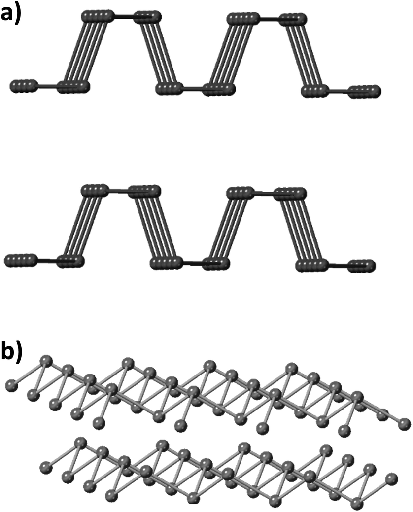 | ||
| Fig. 1 (a) Orthorhombic crystal structure and (b) rhombohedral crystal structure. The first crystal structure is the thermodynamically stable form of phosphorus at room temperature and normal pressure while the rhombohedral structure is the most common for antimony, bismuth and arsenic. | ||
Arsenic (As) has been widely known as a highly toxic material, but it is essential for human life requiring up to 25 μg per day.24 Furthermore, arsenic is mainly employed in the car industry for strengthening the lead components of car batteries25 and it is a common n-type dopant found in a wide range of semiconducting materials.26
At ambient pressures, arsenic is a covalently bonded compound existing in the rhombohedral (A7) phase called grey arsenic (g-As). In addition, arsenic can be found in two more allotropes: yellow arsenic (y-As) and black arsenic (b-As). y-As comprises of tetrahedral As4 molecules similar to white phosphorus (P4),27 while b-As crystallizes in an orthorhombic structure isostructural to black phosphorus (BP).28 A single layer of black arsenic, b-arsenene, has been theoretically calculated to possess a large bandgap,29 which in combination with its low thermal conductivity30 render it as a promising material for thermoelectric applications31 and vapor sensing.32 Thus, black arsenic has been termed as the “cousin” of black phosphorus.
The rhombohedral A7 structure is characteristic of heavy pnictogens which are referred to as grey arsenic, grey antimony and metallic bismuth. It is a low symmetry, three-fold coordinated, and layered structure. The layers are stacked in the (111) direction and consist of puckered, six-membered rings of coordinated atoms in a similar fashion to carbon atoms in graphene sheets.33 The differences between in-plane and out-of-plane interatomic distances are adequately high to provide the layered structure with an anisotropy of the physical properties. Subjected to sufficiently high pressures, arsenic undergoes a transition from a semi-metallic A7 to a metallic simple cubic structure.34 Despite the layered nature of A7, there are notable interlayer interactions of arsenic orbitals across layers leading to partially covalent bonds in the out-of-plane direction. This has a significant effect on the properties of the material especially in performance of the exfoliation procedure, where a lower degree of anisotropy can lead to a lateral size reduction of the exfoliated materials.11
On the other hand, the orthorhombic structure of b-As is composed of puckered layers held together by weak van der Waals forces similar to graphite and black phosphorus.35 This structure is unique for the structural anisotropy inside its layers, which is very rare among 2D materials. Hence, the anisotropy in the physical properties may lead to remarkable device applications which are not possible with isotropic materials.
Shear force exfoliation of grey arsenic has already been demonstrated through the use of kitchen blenders22 and in aqueous surfactant sodium cholate36 and more recently in various organic solvents.37 Herein, we report an effective acetonitrile-assisted exfoliation procedure for black and grey arsenic forming a stable dispersion in acetonitrile. Acetonitrile has been chosen as the exfoliating solvent because it has been used previously for the successful exfoliation of black phosphorus, it has a low boiling point, it can keep a stable dispersion of the exfoliated flakes, prevent the degradation of the exfoliated sheets due to oxidation and can be easily removed without leaving any impurities.38
Both exfoliated materials were characterized in detail showing the presence of single and few layer sheets. The exfoliated arsenene samples in both allotropic modifications were used for gas sensing applications and photothermal absorption experiments. These results will open up new horizons for the fabrication of arsenic-based nanodevices.
Experimental procedure
Materials
Grey (rhombohedral) arsenic was obtained from Alfa Aesar (99.9999%). Black (orthorhombic) arsenic was used in its natural form (Arsenolamprite; Copiapó, Atacama Desert, Chile) of sheet crystals with a 5–10 mm size. Both arsenic allotropes were ground in an agate mortar and sieved to separate particles below 0.5 mm. High-energy shear force exfoliation was performed in dry deoxygenated acetonitrile under an argon atmosphere using 100 mL of acetonitrile and 1 g of arsenic. Firstly, both arsenic samples were dispersed by ultrasonication (10 minutes, 400 W) and subsequently milled at 16![[thin space (1/6-em)]](https://www.rsc.org/images/entities/char_2009.gif) 000 rpm for 2 hours with continuous purging of argon. The prepared suspensions were stored in a glovebox under an argon atmosphere.
000 rpm for 2 hours with continuous purging of argon. The prepared suspensions were stored in a glovebox under an argon atmosphere.
Scanning electron microscopy and energy dispersive spectroscopy
The morphology of the material was investigated via a SEM with a field emission gun electron source (Tescan Lyra dual microscope) and elemental composition and maps of the materials were obtained using an EDS analyzer (X-MaxN) with a 20 mm2 SDD detector (Oxford Instruments) and AZtecEnergy software. The samples were dropcast on a gold plate after being mixed in an acetonitrile solution. SEM and EDS measurements were carried out using an electron beam in the range of 5–15 kV.Transmission electron microscopy
High-resolution TEM was performed with an EFTEM Jeol 2200 FS microscope (Jeol, Japan). A 200 keV acceleration voltage was used for measurement. Elemental maps were acquired with a SDD detector X-MaxN 80 TS (Oxford Instruments, England). All samples prior to the measurements were put on a TEM grid (Cu; 200 mesh; Formvar/carbon).X-ray photoelectron spectroscopy
XPS measurements were performed using an ESCAProbeP spectrometer (Omicron Nanotechnology Ltd, Germany) employing a monochromatic aluminum X-ray radiation source (1486.7 eV). Wide-scan surveys of all elements were performed with subsequent high-resolution scans of arsenic (As 3d). The samples were placed on a conductive carrier made from a high purity silver bar. For elimination of the sample charging during measurement an electron gun was utilized (1–5 V). All the XPS survey spectra were afterwards analyzed by CasaXPS software.Atomic force microscopy
The AFM measurements were carried out on an Ntegra Spectra from NT-MDT. The surface scans were performed in a tapping (semi-contact) mode. Cantilevers with a strain constant of 1.5 kN m−1 equipped with a standard silicon tip with a curvature radius lower than 10 nm were used for all measurements. For the measurements the sample suspension (1 mg mL−1) was drop-cast on a freshly cleaved mica substrate. The measurements were performed under ambient conditions with a scan rate of 1 Hz and a scan line of 512.X-ray diffraction
XRD patterns were acquired using a Bruker D8 Discoverer powder diffractometer (Bruker, Germany) in Bragg–Brentano parafocusing geometry and applying Cu Kα radiation (λ = 0.15418 nm and U = 40 kV, I = 40 mA). The diffraction patterns were collected between 5° and 90° of 2θ with a step size of 0.020° and the acquired data were evaluated using HighScore Plus 3.0e.Raman spectroscopy
The Raman spectra were taken using an inVia Raman microscope (Renishaw, England) in backscattering geometry with a CCD detector and a DPSS laser (532 nm, 50 mW) with an applied power of 5 mW and a 50× magnification objective. A small amount of each of the samples was placed on a piece of silicon wafer.Density functional theory (DFT)
DFT calculations were performed using the projector-augmented wave method as implemented in the Vienna ab initio simulation package (VASP).39,40 The energy cut-off for the plane-wave expansion was set to 300 eV. The optimized van der Waals optB86b-vdW functional41,42 was used because it provided accurate structural properties of various materials combining string intralayer interactions including BP.43–45 The calculated lattice parameters were a = 3.74, b = 4.46 and c = 11.02 Å, in excellent agreement with the available experimental data. A dense k-point sampling of 16 × 16 × 16 for the A7 structure of g-As and 12 × 10 × 6 mesh for orthorhombic b-As were employed. The elements of the force-constant matrix for the calculation of vibrational modes were determined using density functional perturbation theory. Each mode's off-resonance Raman activity was calculated by evaluating the derivative of the polarizability (or macroscopic dielectric tensor) with respect to the pertinent mode coordinate using the Raman-sc package. The symmetry analysis of an irreducible representation of active modes was performed using the Phonopy package.46Fourier transform-infrared spectroscopy
FT-IR measurements were performed on an iS50R FTIR spectrometer (Thermo Scientific, USA). The measurement was performed with a diamond ATR crystal, a DLaTGS detector and a KBr beamsplitter in the range 4000–400 cm−1 at a resolution of 4 cm−1. The measurement was performed in reflectance mode using a Smart SAGA reflectance accessory and a MCTD* detector and a KBr beamsplitter. The sample for measurement was prepared by drying the dispersion on a gold coated silicon substrate. The measurement of transmittance in the NIR region was performed with a CaF2 beamsplitter and with a liquid nitrogen cooled MCT-D* detector.Photothermic effect
From As nanoparticles, suspensions were prepared in water resulting in 0.1, 0.25 and 1 mg mL−1 concentrations of As. Additionally, 200 μL of Tween was added to suppress the sedimentation of nanoparticles. Before measurement, the tested suspension was sonicated for 5 min. Subsequently, the suspension was irradiated using a laser diode of 880 nm (0.8 W cm−2) as biological tissues are most transparent in the 800–900 nm spectral band47 and the temperature was recorded using a Pt-100 resistive sensor.Electrochemical impedance spectroscopy (EIS)
The characterization by EIS was performed using an Autolab PGSTAT 204 (Metroohm, Switzerland) equipped with a FRA 32M impedance module. Gold interdigitated electrodes (4 μm lines and spacing) were used for the impedimetric electrochemical detection of volatile organic compounds. A sinusoidal potential modulation with an amplitude of 10 mV at a potential of 0.0 V was used to achieve linearity conditions. Applied frequency ranged from 1 MHz to 1 Hz with 10 measured points per decade.The samples were dispersed in acetonitrile to obtain a 2 mg mL−1 suspension (Fig. 2a). The suspension was sonicated for 5 min at room temperature before the use. An interdigitated electrode was modified by drop-casting of a 50 μL aliquot of the suspension which was dried for 15 min in a vacuum oven at 55 °C to obtain a layer of randomly dispersed materials on the electrode surface. The electrodes were tested by cyclic voltammetry to verify conductivity of the modified electrodes and to achieve linearity conditions prior to the EIS measurements. The modified electrodes were left in a vacuum oven for 15 min before every single EIS measurement. A 50 mL flask was used as the electrochemical cell. The flask was filled with 50 μL of the investigated compound, sealed and left to equilibrate for 120 s to achieve steady state conditions.
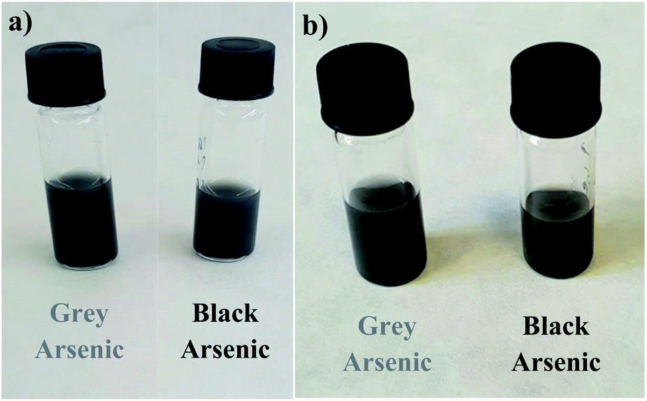 | ||
| Fig. 2 Suspensions of exfoliated grey (left) and black (right) arsenic in acetonitrile (a) after 1 hour and (b) after 8 days. | ||
Results and discussion
Characterization of materials
The phase purity of the starting materials was identified by X-ray diffraction confirming the rhombohedral and orthorhombic structures for grey and black arsenic, respectively (PDF 04-003-6953 and 03-065-2495) (Fig. S1†). These arsenic allotropes were exfoliated in acetonitrile by high-energy shear force milling and the prepared suspensions of single/few layer of each respective material were used for further characterization and application exploration. Both materials had a stable dispersion for 8 days as pure acetonitrile is capable of effectively stabilizing exfoliated arsenene37 (Fig. 2b). The process of the exposure of exfoliated arsenic materials to ambient conditions is shown in Fig. S2† where their stability after 8 days and degradation after 9 days are shown. The degradation of the suspensions after 9 days can be observed from the clear sedimentation of the material and the solution became more transparent.The morphology of bulk grey and black arsenic used for exfoliation is shown in Fig. S3.† On both materials a layered structure is clearly observed with small pieces due to the materials having been mechanically ground prior to the measurements.
After the exfoliation of both materials in acetonitrile, AFM images were acquired to observe the thickness. In Fig. S4,† the images accompanied by the measured height profile are depicted. It becomes evident that the exfoliation procedure for b-As is more efficient producing arsenic nanosheets with a thickness below 3 nm in comparison to the g-As nanosheets possessing a thickness between 20 and 30 nm. Despite the approximately similar bond lengths of arsenic atoms in both materials, the distance between layers is larger in b-As (Table S1†). This is caused by the orthorhombic nature of the b-As structure as the layers are held together by weak van der Waals forces in contrast to the rhombohedral structure of g-As, where the layers are held together more tightly.
Additional characterization was carried out through TEM combined with selected area electron diffraction (SAED) and EDS. TEM images revealed a sheet structure for both materials and the SAED patterns of sheets showed the rhombohedral and orthorhombic structures for grey and black arsenic, respectively (Fig. 3). The SEM/EDS and TEM/EDS images exposed the uniform presence of arsenic over the sheets including the presence of oxygen in both materials (Fig. S5 and S6†). Nevertheless, since the distribution does not resemble the As elemental maps, it was concluded that the presence of oxygen is due to atmospheric contamination and that possible oxide formation is local. Therefore, according to the EDS elemental maps from TEM we have confirmed the existence of few-layered arsenene and excluded the formation of arsenic oxide on the exfoliated sheets.
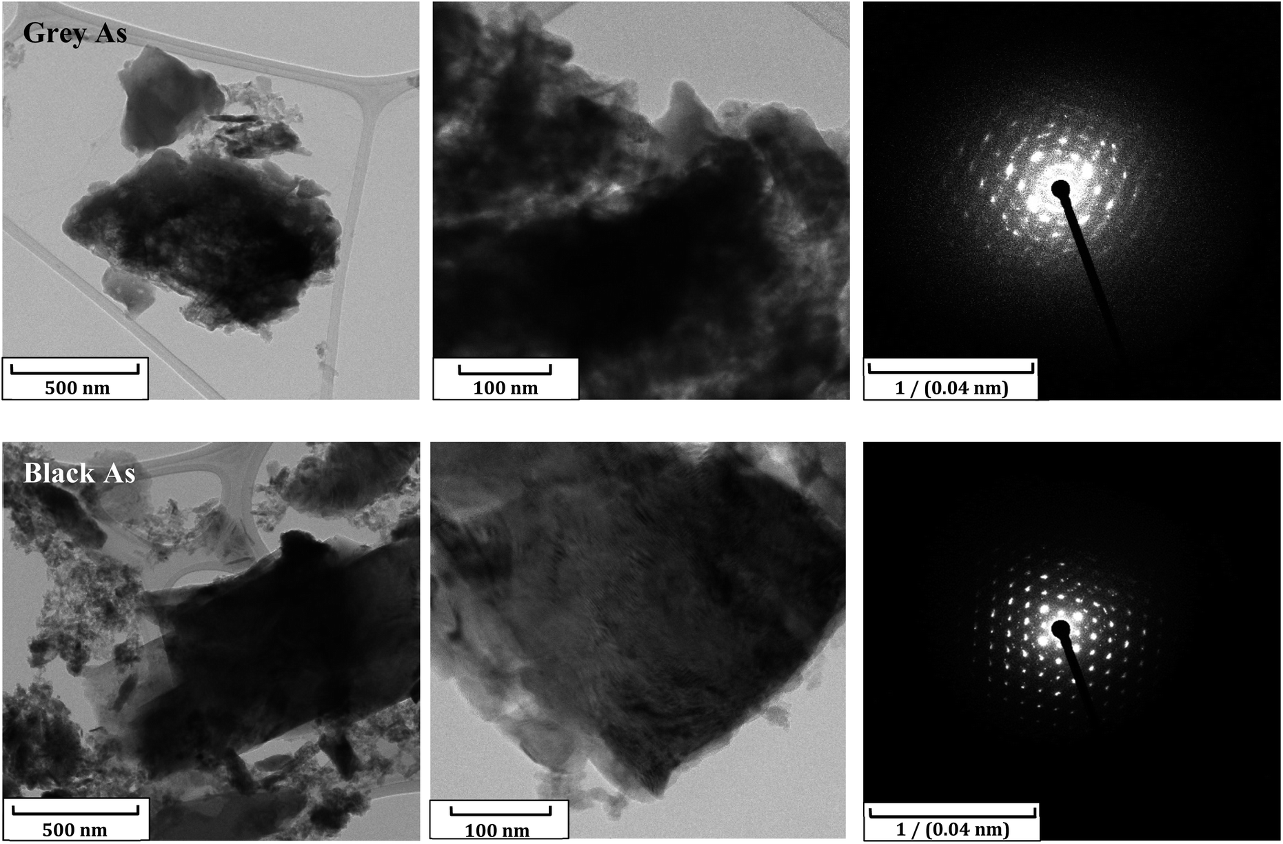 | ||
| Fig. 3 TEM/SAED of grey and black arsenic nanoparticles. | ||
The surface composition of exfoliated black and grey arsenic was examined by XPS, a useful technique to examine the oxidation state of arsenic within a material. The wide-survey spectra confirmed the presence of arsenic in both materials (Fig. S7†). Adventitious carbon is also present along with oxygen originating from either atmospheric contamination or arsenic oxide (As2O3) formation on the surface of the materials.
In addition, Fig. 4 shows the comparison of the high-resolution XPS spectrum of As 3d between exfoliated grey and black arsenic. Two distinguishable peaks clearly formed for both materials. The sharp peak at 42.2 eV corresponds to the As–As binding energy of elemental arsenic22,48 while the signal at 44.9 eV is due to the inevitable formation of As2O3 on the material surface caused by the atmospheric oxygen. According to the XPS results, it is likely that black arsenic is less susceptible to oxidation as evidenced by the calculated As:As2O3 ratio presented in Table 1. However, it is a well-known fact that arsenic trioxide sublimes in a vacuum49 and that the previous results demonstrate the high tendency of arsenic towards oxidation. This effect is also well known from the surface chemistry of black phosphorus, which undergoes rapid formation of phosphorus oxides on the surface.50
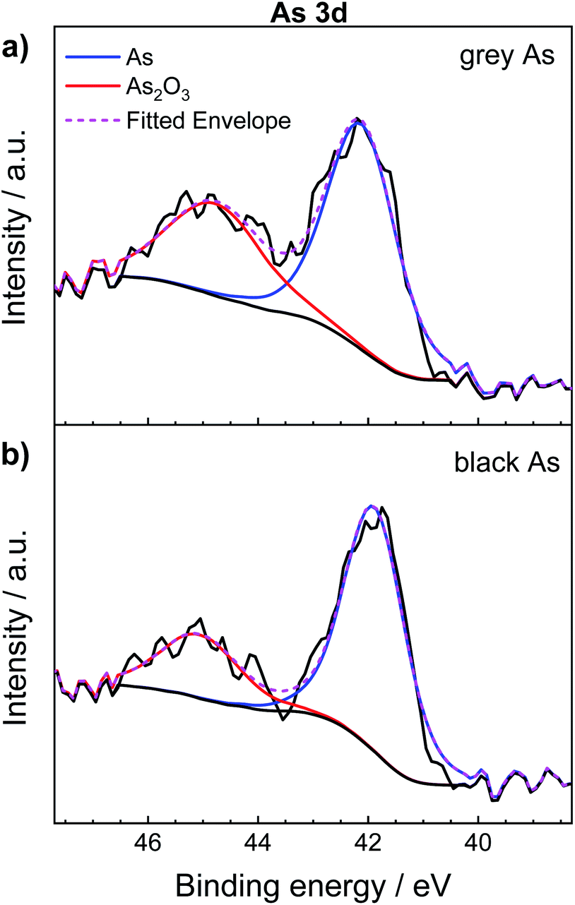 | ||
| Fig. 4 High-resolution As 3d XPS spectra of (a) grey arsenic and (b) black arsenic. | ||
| Material | %As | %As2O3 | As/As3+ ratio |
|---|---|---|---|
| Grey arsenic | 62.70 | 37.30 | 1.68 |
| Black arsenic | 73.59 | 26.41 | 2.78 |
Both exfoliated allotropes of arsenic were further explored by X-ray diffraction (Fig. 5). Firstly, the rhombohedral R![[3 with combining macron]](https://www.rsc.org/images/entities/char_0033_0304.gif) m crystal structure of grey arsenic (PDF 01-073-5919) was confirmed with the most intense diffraction pattern at 2θ = 32.2° corresponding to the (012) reflection. Some minor peak diffraction pattern noticeable in the XRD pattern had arisen due to the presence of As2O3.
m crystal structure of grey arsenic (PDF 01-073-5919) was confirmed with the most intense diffraction pattern at 2θ = 32.2° corresponding to the (012) reflection. Some minor peak diffraction pattern noticeable in the XRD pattern had arisen due to the presence of As2O3.
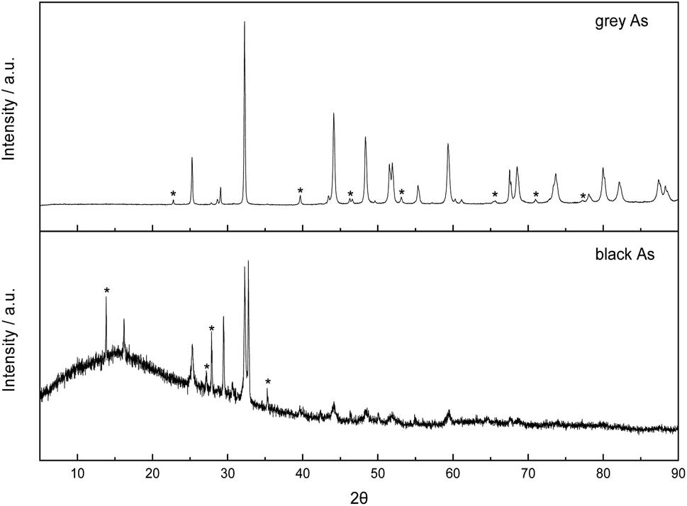 | ||
| Fig. 5 Comparison of X-ray diffraction patterns of exfoliated grey and black arsenic. Peaks marked with an asterisk are due to the presence of arsenic oxide in the sample. | ||
Regarding the XRD pattern of the exfoliated black arsenic, the non-flat baseline is indicative of the presence of amorphous arsenic also visible in the SEM images. The most prominent feature is a sharp doublet peak at 2θ of 32.55 and 32.80° characteristic of the allotropic orthorhombic crystal structure of arsenic (PDF 00-029-0142) and corresponding to the (004) and (111) phases, respectively. However, the presence of arsenic oxide is much more pronounced in the black As XRD pattern where the relevant peaks are more intense in comparison to the pattern of grey As and there were also some minor peaks arising due to rhombohedral arsenic. Finally, the sharp narrow peaks in both patterns revealed the high crystallinity of the materials.
The structural differences between grey and black arsenic were further examined by Raman spectroscopy and depicted in Fig. 6. The A7 structure of g-As belongs to the Rm space group which has three Raman active modes, a two-fold degenerate Eg and A1g. The modes are clearly visible at 202 and 254 cm−1.51 The DFT calculations confirm the presence of two active modes where the calculated wavenumbers of the modes are 184 and 245 cm−1. For vibrations perpendicular to the layers of the rhombohedral lattice, the A1g mode belongs to a pure longitudinal motion of the atom planes, whereas two Eg modes correspond to transverse motions.
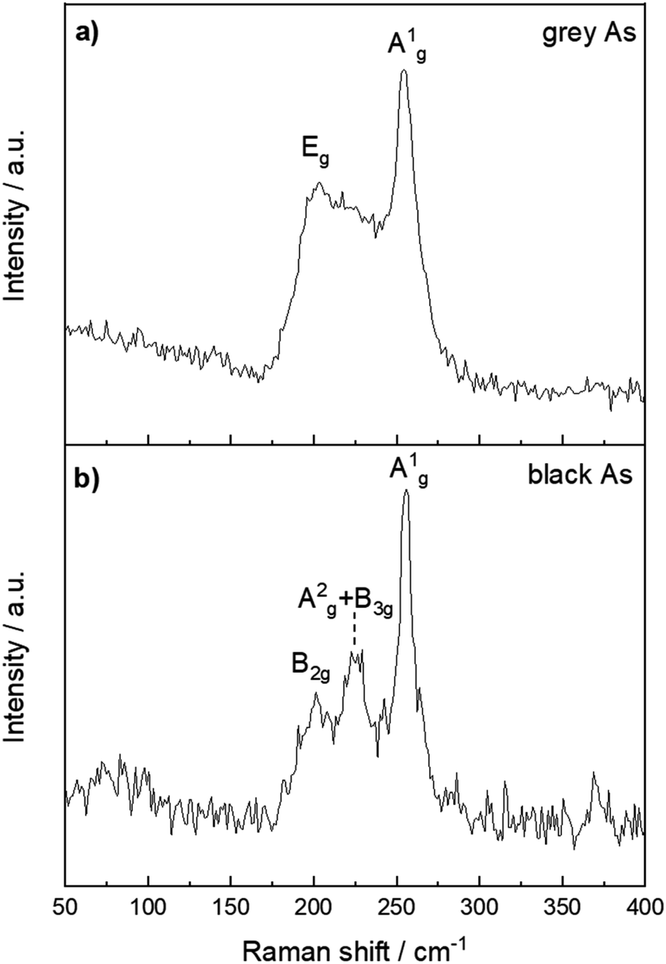 | ||
| Fig. 6 Raman spectra of (a) black arsenic and (b) grey arsenic with their respective phonon modes labelled. | ||
The structure of b-As has the Cmca (no. 64) space group and there are 12 lattice vibrational modes at the G point. According to the character table, six of them should be Raman active with the irreducible representations 2Ag + B1g + B2g + 2B3g. The Raman spectrum in Fig. 6b nevertheless reveals three distinct peaks at 201, 223 and 255 cm−1. Three phonon modes were observed also in an earlier study of b-As as well35 at slightly shifted frequencies (224, 230 and 258 cm−1) and possess similar features to the well-indexed Raman spectrum of black phosphorus.52 Our DFT calculations yield six Raman active modes at 90, 104, 206, 216, 228 and 239 cm−1, in agreement with the symmetry considerations above. For an irreducible representation of each mode, we assign them to the out-of-plane B1g, B3g, B2g, A2g and in-plane B3g and A1g in the respective order. The less intense modes at 90 and 104 cm−1 are not visible in the spectrum due to the background noise. The A2g and B3g modes at 216 and 228 cm−1 are most likely convoluted in the Raman spectrum and give rise to a broad middle peak. Thus, the three peaks in the spectrum confirm the orthorhombic crystal structure of the material. It should be noted that owing to the anisotropic character of the structure. The relative intensity of the mode's Raman shifts depends on the sample orientation with respect to the direction and polarization of the incident laser light.35,53
Photothermic effect
In the next step, potential applications of arsenic nanoparticles were explored. Firstly, the photothermic effect was evaluated using an 880 nm laser irradiation. Three different arsenic concentrations were tested and pure water for comparison (Fig. 7). While pure water exhibited only a negligible increase in temperature, all arsenic suspensions showed fast elevation during the first 5 minutes and afterwards, the temperature was gradually increasing until it reached a maximum temperature plateau. After 20 minutes, black As reached final temperatures of 45, 51 and 56 °C and grey As reached 52, 55 and 58 °C for As concentrations of 0.1, 0.25 and 1 mg mL−1, respectively. Thus, both samples exhibited a similar photothermic effect.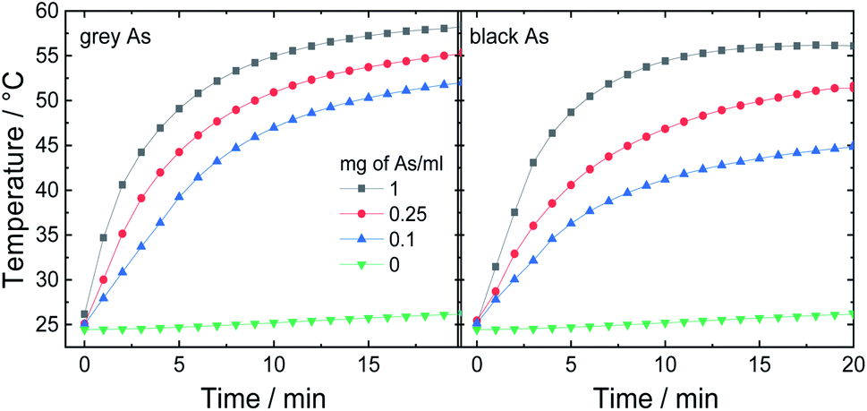 | ||
| Fig. 7 Photothermic effect measured on three different As concentrations using an 880 nm (0.8 W cm−2). | ||
Gas sensing
Lastly, the potential application of the prepared samples as impedimetric sensors for volatile organic compounds (VOCs) was investigated. Both arsenic samples were dropcast on gold interdigitated electrodes. Between the gold electrode and the active material, two types of contacts can exist – ohmic or Schottky. First of all, a cyclic voltammogram was obtained in the range between −1.5 and 1.5 V to distinguish which type of transition is present (Fig. S8†). Grey As exhibited a linear current–voltage (I–V) curve in the whole potential range due to its metallic character thus this sensor exhibits an ohmic transition. On the other hand, black As exhibited Schottky transition and has a nonlinear I–V curve.Following this, the modified interdigitated electrodes were exposed to various VOCs and ambient air for comparison and the impedimetric responses were collected. These responses are displayed as Bode and Nyquist plots (Fig. 8 and S9†, respectively). The Bode plot shows frequency dependence of phase shift which can be utilized to differentiate between individual VOCs. Grey As showed sensitivity towards two VOCs: methanol and ethanol with maxima of phase shift at 9 (−21°) and 6 kHz (−7°), respectively. Black As was sensitive towards five VOCs: methanol, ethanol isopropanol, acetone and acetonitrile with maxima of phase shift at 400 (−80°), 400 (−77°), 500 (−71°), 80 (−60°) and 13 (−12°) Hz, respectively. Moreover, the stability of the impedimetric sensors was evaluated by a repetition of measurements in ambient air after the exposure to the tested VOCs (Fig. S10†). Only slight shifts of the measured points were observed that confirmed the good stability of the tested impedimetric sensors.
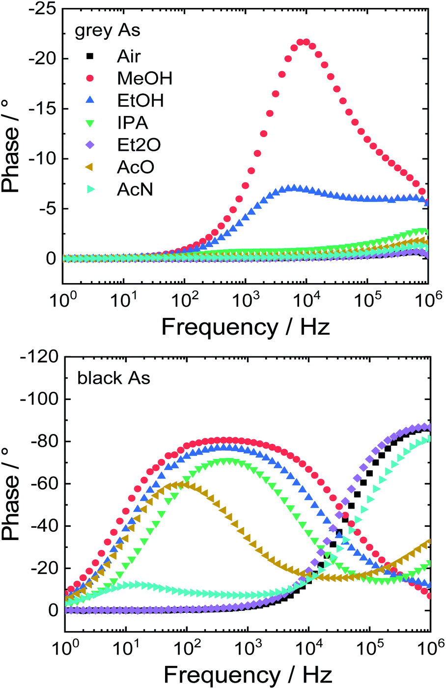 | ||
| Fig. 8 Response of impedimetric sensors to various VOCs plotted as Bode diagrams. | ||
Conclusion
In summary, compelling experimental evidence has been demonstrated for a novel exfoliation method of grey and black arsenic nanoparticles. SEM images revealed the existence of ordered stacked layers for both arsenic samples while structural characterization confirmed the orthorhombic and rhombohedral structures of black and grey arsenic before and after exfoliation. Additionally, both exfoliated samples were tested for potential applications in photothermic absorption and as impedimetric sensors of VOCs. While both samples exhibited a similar photothermic effect, exfoliated black arsenic was revealed to be more suitable as an impedimetric VOC sensor.Conflicts of interest
The authors do not have any conflicts of interest.Acknowledgements
The project was supported by Czech Science Foundation (GACR No. 19-26910X). P. L. acknowledges the support of the Ministry of Education, Youth and Sports of the Czech Republic under Project No. LO1305 and the Operational Programme for Research, Development and Education of the European Regional Development Fund (Project No. CZ.02.1.01/0.0/0.0/16_019/0000754).References
- K. S. Novoselov, A. K. Geim, S. V. Morozov, D. Jiang, Y. Zhang, S. V. Dubonos, I. V. Grigorieva and A. A. Firsov, Science, 2004, 306, 666–669 CrossRef CAS PubMed.
- K. S. Novoselov, A. K. Geim, S. V. Morozov, D. Jiang, M. I. Katsnelson, I. V. Grigorieva, S. V. Dubonos and A. A. Firsov, Nature, 2005, 438, 197–200 CrossRef CAS PubMed.
- Y. B. Zhang, Y. W. Tan, H. L. Stromer and P. Kim, Nature, 2005, 438, 201–204 CrossRef CAS PubMed.
- J. N. Coleman, M. Lotya, A. O'Neill, S. D. Bergin, P. J. King, U. Khan, K. Young, A. Gaucher, S. De, R. J. Smith, I. V. Shvets, S. K. Arora, G. Stanton, H. Y. Kim, K. Lee, G. T. Kim, G. S. Duesberg, T. Hallam, J. J. Boland, J. J. Wang, J. F. Donegan, J. C. Grunlan, G. Moriarty, A. Shmeliov, R. J. Nicholls, J. M. Perkins, E. M. Grieveson, K. Theuwissen, D. W. McComb, P. D. Nellist and V. Nicolosi, Science, 2011, 331, 568–571 CrossRef CAS.
- L. Chen, B. Liu, A. Abbas, Y. Ma, X. Fang, Y. Liu and C. Zhou, ACS Nano, 2014, 8, 11543–11551 CrossRef CAS PubMed.
- B. Radisavljevic, A. Radenovic, J. Brivio, V. Giacometi and A. Kis, Nat. Nanotechnol., 2011, 6, 147–150 CrossRef CAS.
- Y. Zhang, T. R. Chang, B. Zhou, Y. T. Cui, H. Yan, Z. K. Liu, F. Scmitt, J. Lee, R. Moore, Y. L. Chen, H. Lin, H. T. Jeng, S. K. Mo, Z. Hussain, A. Bansil and Z. X. Shen, Nat. Nanotechnol., 2014, 9, 111–115 CrossRef CAS.
- S. Najmaei, Z. Liu, W. Zhou, X. L. Zou, G. Shi, S. D. Lei, B. I. Yakobson, J. C. Idrobo, P. M. Ajayan and J. Lou, Nat. Mater., 2013, 12, 754–759 CrossRef CAS PubMed.
- B. Liu, L. Chen, G. Liu, A. Abbas, M. Fathi and C. Zhou, Nat. Mater., 2014, 8, 5304–5314 CAS.
- L. Li, Y. Yu, G. J. Ye, Q. Ge, X. Ou, H. Wu, D. Feng, X. H. Chen and Y. Zhang, Nat. Nanotechnol., 2014, 9, 372–377 CrossRef CAS PubMed.
- F. Xia, H. Wang and Y. Jia, Nat. Commun., 2014, 5, 4458 CrossRef CAS.
- H. O. H. Churchill and P. Jarillo-Herrero, Nat. Nanotechnol., 2014, 9, 330–331 CrossRef CAS PubMed.
- Y. Zhang, A. Rubio and G. Le Lay, J. Phys. D: Appl. Phys., 2017, 50, 053004 CrossRef.
- D. Geng and H. Y. Yang, Adv. Mater., 2018, 30, e1800865 CrossRef PubMed.
- J. R. Brent, N. Savjani, E. A. Lewis, S. J. Haigh, D. J. Lewis and P. O'Brien, Chem. Commun., 2014, 50, 13338–13341 RSC.
- J. B. Smith, D. Hagaman and H.-F. Ji, Nanotechnology, 2016, 27, 215602 CrossRef PubMed.
- S. P. Koenig, R. A. Doganov, H. Schmidt, A. H. C. Neto and B. Ozyilmaz, Appl. Phys. Lett., 2014, 104, 103106 CrossRef.
- A. Ng, T. E. Sutto, B. R. Matis, Y. Deng, P. D. Ye, R. M. Stroud, T. H. Brintlinger and N. D. Bassim, Nanotechnology, 2017, 28, 155601 CrossRef CAS PubMed.
- F. Reis, G. Li, L. Dudy, M. Bauernfeind, S. Glass, W. Hanke, R. Thomale, J. Schäfer and R. Claessen, Science, 2017, 357, 287–290 CrossRef CAS PubMed.
- M.-Y. Liu, Y. Huang, Q.-Y. Chen, Z.-Y. Li, C. Cao and Y. He, RSC Adv., 2017, 7, 39546 RSC.
- G. Wang, R. Pandey and S. P. Karna, ACS Appl. Mater. Interfaces, 2015, 7, 11490–11496 CrossRef CAS PubMed.
- R. Gusmão, Z. Sofer, D. Bouša and M. Pumera, Angew. Chem., Int. Ed., 2017, 56, 14417–14422 CrossRef PubMed.
- L. Cartz, S. R. Srinivasa, R. J. Riedner, J. D. Jorgensen and T. G. Worlton, J. Chem. Phys., 1979, 71, 1718–1721 CrossRef CAS.
- D. R. Mayer, W. Kosmus, H. Pogglitsch, D. Mayer and W. Beyer, Biol. Trace Elem. Res., 1993, 37, 27–38 CrossRef CAS PubMed.
- A. G. Milnes and A. Y. Polyakov, Mater. Sci. Eng., B, 1993, 18, 237 CrossRef.
- N. E. Bagshaw, J. Power Sources, 1995, 53, 25 CrossRef CAS.
- A. Bettendorff, Liebigs Ann. Chem., 1867, 144, 110 CrossRef.
- P. M. Smith, A. J. Leadbetter and A. J. Apling, Philos. Mag., 1975, 31, 57 CrossRef CAS.
- S. Zhang, Z. Yan, Y. Li, Z. Chen and H. Zeng, Angew. Chem., Int. Ed., 2015, 54, 3112–3115 CrossRef CAS.
- D. P. Jones, N. Thomas and W. A. Phillips, Philos. Mag. B, 1978, 38, 271 CAS.
- S. Sharma, S. Kumar and U. Schwingensclögl, Phys. Rev. Appl., 2017, 8, 044013 CrossRef.
- S. M. Beladi-Mousavi, A. M. Pourrahimi, Z. Sofer and M. Pumera, Adv. Funct. Mater., 2018, 29, 1807004 CrossRef.
- G. N. Greaves, S. R. Elliott and E. A. Davis, Adv. Phys., 1979, 28, 49 CrossRef CAS.
- P. Silas, J. R. Yates and P. D. Haynes, Phys. Rev. B: Condens. Matter Mater. Phys., 2008, 78, 174101 CrossRef.
- Y. Chen, C. Chen, R. Kealhofer, H. Liu, Z. Yuan, L. Jiang, J. Suh, J. Park, C. Ko, H. S. Choe, J. Avila, M. Zhong, Z. Wei, J. Li, H. Gao, Y. Liu, J. Analytis, Q. Xia, M. C. Asensio and J. Wu, Adv. Mater., 2018, 30, 1800754 CrossRef PubMed.
- H. L. Chia, N. M. Latiff, R. Gusmão, Z. Sofer and M. Pumera, Chem.–Eur. J., 2019, 25, 2242 CrossRef CAS PubMed.
- Z.-H. Qi, Y. Hu, Z. Jin and J. Ma, Phys. Chem. Chem. Phys., 2019, 21, 12087–12090 RSC.
- A. E. Del Rio Castillo, V. Pellegrini, H. Sun, J. Buha, D. A. Dinh, E. Lago, A. Ansaldo, A. Capasso, L. Manna and F. Bonaccorso, Chem. Mater., 2018, 30, 506–516 CrossRef CAS.
- P. E. Blöchl, Phys. Rev. B: Condens. Matter Mater. Phys., 1994, 50, 17953–17979 CrossRef PubMed.
- G. Kresse and D. Joubert, Phys. Rev. B: Condens. Matter Mater. Phys., 1999, 59, 1758–1775 CrossRef CAS.
- J. Klimeš, D. R. Bowler and A. Michaelides, J. Phys.: Condens. Matter, 2010, 22, 022201 CrossRef PubMed.
- J. Klimeš, D. R. Bowler and A. Michaelides, Phys. Rev. B: Condens. Matter Mater. Phys., 2011, 83, 195131 CrossRef.
- P. Lazar, J. Martincová and M. Otyepka, Phys. Rev. B: Condens. Matter Mater. Phys., 2015, 92, 224104 CrossRef.
- P. Lazar, E. Otyepková, M. Pykal, K. Čépe and M. Otyepka, Nanoscale, 2018, 10, 8979–8988 RSC.
- Z. Sofer, J. Luxa, D. Bouša, D. Sedmidubský, P. Lazar, T. Hartman, H. Hardtdegem and M. Pumera, Angew. Chem., Int. Ed., 2017, 56, 9891–9896 CrossRef CAS PubMed.
- A. Togo and I. Tanaka, Scr. Mater., 2015, 108, 1–5 CrossRef CAS.
- E. V. Samsonova, A. V. Popov, A. S. Vanetsev, K. Keevend, E. O. Orlovskaya, V. Kiisk, S. Lange, U. Joost, K. Kaldvee, U. Mäeorg, N. A. Glushkov, A. V. Ryabova, I. Sildos, V. V. Osiko, R. Steiner, V. B. Loschenov and Y. V. Orlovskii, Phys. Chem. Chem. Phys., 2014, 16, 26806–26815 RSC.
- S. C. Ghosh, M. C. Biesinger, R. R. LaPierre and P. Kruse, J. Appl. Phys., 2007, 101, 114322 CrossRef.
- R. Pöttgen and D. Johrendt, Intermetallics, Walter de Gruyter GmbH, Berlin/Boston, 2014 Search PubMed.
- J. O. Island, G. A. Steele, H. S. J. van der Zant and A. Castellanos-Gomez, 2D Mater., 2015, 2, 01102 Search PubMed.
- P. Vishnoi, M. Mazumder, S. K. Pati and C. N. R. Rao, New J. Chem., 2018, 42, 14091–14095 RSC.
- S. Sugai and I. Shirotani, Solid State Commun., 1985, 53, 753–755 CrossRef CAS.
- J. Wu, N. Mao, L. Xie, H. Xu and J. Zhang, Angew. Chem., Int. Ed., 2015, 54, 2366–2369 CrossRef CAS PubMed.
Footnote |
| † Electronic supplementary information (ESI) available. See DOI: 10.1039/c9na00754g |
| This journal is © The Royal Society of Chemistry 2020 |