
 Open Access Article
 This Open Access Article is licensed under a Creative Commons Attribution-Non Commercial 3.0 Unported Licence
Two-dimensional Bi2Se3 nanosheet based flexible infrared photodetector with pencil-drawn graphite electrodes on paper
Shengqian
Liu
,
Zongyu
Huang
 *,
Hui
Qiao
,
Rong
Hu
,
Qian
Ma
,
Kai
Huang
,
Hongxing
Li
and
Xiang
Qi
*
*,
Hui
Qiao
,
Rong
Hu
,
Qian
Ma
,
Kai
Huang
,
Hongxing
Li
and
Xiang
Qi
*
Hunan Key Laboratory of Micro-Nano Energy Materials and Devices, Laboratory for Quantum Engineering and Micro-Nano Energy Technology, School of Physics and Optoelectronic, Xiangtan University, Hunan 411105, P. R. China. E-mail: zyhuang@xtu.edu.cn; xqi@xtu.edu.cn
First published on 4th January 2020
Abstract
Flexible optoelectronic devices have been of great significance in recent years, owing to their extensive commercial and military applications. However, the manufacturing processes of most existing flexible photodetectors are particularly complicated and expensive. Employing a facile and low cost way for constructing a high performance flexible infrared photodetector is one of the effective strategies to facilitate its practical applications. Pencil-drawing is a popular method in novel electronic and optoelectronic devices, as it is a low cost and facile fabrication process. Herein, we report a novel flexible infrared photodetector using liquid-exfoliated Bi2Se3 nanosheets as a light sensitive material, pencil-drawn graphite as the electrodes, and paper as the substrate. The as-fabricated photodetector exhibits high photocurrent, excellent responsivity and long-term stability under 1064 nm infrared light irradiation. In addition, as the pencil-drawn photodetector is made of a flexible paper substrate, it also well exhibits stability and durability under bending conditions. This work is proposed to be a route to construct a novel flexible infrared photodetector with a facile manufacturing process and low cost.
1. Introduction
To date, infrared (IR) photodetectors have drawn extensive attention from worldwide researchers owing to their various applications in military and daily life, such as human healthcare,1 detection of gas leakages,2 security monitoring3 and consumer electronic products.4 Interestingly, there is a notable tendency to make flexible photodetectors based on lightweight substrates more portable and wearable in modern society, which is clearly reflected in the microchips of almost every smart electronic device, such as flexible mobile phones and large-area foldable displays. Thus, there is an urgent need to fabricate a novel flexible photodetector with ultra-high responsivity and stability that can satisfy the increasing demands of portable commercial facilities. However, the corresponding technical requirements restrict the practical application of the devices. Most existing photodetectors are rigid and difficult to integrate with other functional components. Therefore, state-of-the-art infrared photodetectors require intrinsically flexible materials that contribute multiple advantages combined with broadband detection and ultra-high responsivity to meet the requirements of sensitivity and flexibility.5–8Recently, two-dimensional (2D) materials have attracted widespread attention in advanced photodetectors due to their inherent atomic structure with excellent flexibility,9 superior photoelectric properties10–12 and high compatibility with flexible substrates. Among them, black phosphorus (BP) is a novel 2D material with an inherent direct bandgap,13 but it is well known that 2D BP is unstable when exposed to ambient conditions, which limits its practical applications.14 Transition metal dichalcogenides (TMDs) have extraordinary electrical and optical properties that evolve from quantum confinement and surface effects.15,16 TMDs can be used in infrared photodetectors by introducing appropriate defects, but the fabrication of devices is very expensive and complicated.17 Besides BP and TMDs, topological insulators (TIs) are considered as a novel class of 2D materials,18 revealing an exotic state of quantum matter with conductive surface states and insulating bulky states with an indirect band gap.19,20 In recent years, topological insulators have aroused the great interest of researchers, owing to their excellent bending ability, superior optoelectronic properties with a layer-dependent band-gap and polarization-sensitive photocurrent,21 enabling them to be widely applied in the new generation of optoelectronic devices.22,23 Bismuth selenide (Bi2Se3), which is one of the topological insulators, has attracted enormous attention from researchers because of its very exciting optoelectronic properties and 0.3 eV bandgap (can be tuned with the layer thickness) as well as high carrier mobility.24–26 Owing to these special properties, Bi2Se3 is a new promising star in the field of photodetection. For example, Wang et al. investigated 2D Bi2Se3 flakes, demonstrating a strong responsivity of 23.8 A W−1 and EQE of 2035% under 1465 nm laser irradiation.27 Zhang et al. fabricated a novel Bi2Se3/Si photodetector with superior responsivity at optical communication wavelength.28 According to the above reports, although great accomplishments in the field of optoelectronic devices have been achieved, it is particularly rigorous and complicated to manufacture Bi2Se3 photodetectors as they are expensive and lack mechanical flexibility, greatly restricting the practical applications of the device. Considering the commercial benefits and practical application issues, all components of the flexible photodetector should be optimized to address the requirements of malleability, portability, environment-friendliness, low-cost and durability. Writing is a state-of-the-art route and has been widely applied in the field of optoelectronics. Cao et al. fabricated a flexible photodetector with a high responsivity of 2.1 A W−1 using pencil-drawn electrodes on paper.29 Zhang et al. demonstrated that a humidity sensor based on pencil-tracing exhibited fast response speeds (1 s) and good long-term stability.30 Graphite is one kind of carbon allotrope, which is known to possess high carrier mobility and is commonly found in pencils. It can be used to easily draw on common paper with a slight force, which is the easiest way to construct graphite electrodes.31 In addition, for flexible devices, common paper is one of the most competitive substrates because of its extremely low-cost, eco-friendly nature and compatibility with other components of the devices. What's more, paper is pliable enough to support flexible devices.
In this work, Bi2Se3 nanosheets were obtained via a simple liquid exfoliation method.32 As-exfoliated materials are utilized as the light absorption layer of the flexible infrared photodetector due to their narrow band gap and high optical absorption coefficient. The novel flexible infrared photodetectors exhibited excellent flexibility, bendability and extendable durability under 1064 nm infrared illumination. It can be mass-produced on common paper using pencils and brushes. It is found that the photocurrent of the flexible IR photodetector can reach 0.82 μA under a low operating voltage of 5 V; the bending stability test demonstrates that the pencil-drawn device shows no significant photocurrent attenuation after 1000 bending cycles and retains 60% of the pristine photocurrent under various bending angles. In addition, the comparison of the Bi2Se3-based photodetector in this work with photodetectors of other reported related materials is shown in Table 1. Some of them have exhibited better performances in terms of their responsivity or response time. However, it is clear that the as-prepared pencil-drawn device based on our Bi2Se3 nanosheets not only involves an even simpler manufacturing process than the previously reported photodetectors, but also exhibits good photoresponse in the near-infrared region, and the pencil-drawn device has superior flexibility and durability owing to its unique features. Herein, we believe that this work has a positive reference value for the design and applications of future wearable infrared devices.
| Device structure | Materials | Wavelength (nm) | Responsivity (μA W−1) | τ r/τf (s) | Flexible | Ref. |
|---|---|---|---|---|---|---|
| a Photoconductive type. b Photoelectrochemical type. c Phototransistors. | ||||||
| ITO/Teb | Te nanosheets | 400 | 2.79 | — | No | 38 |
| ITO/BPb | BP nanosheets | Simulated light | 2.2 | 0.5/1.1 | No | 13 |
| ITO/Bib | Bi quantum dots | 365 | 285.7 | 0.2/0.2 | No | 39 |
| Ag/Bi2Se3/Aga | Bi2S3 nanoflowers | 980 | — | 0.8/3 | Yes | 11 |
| ITO/Bi2S3b | Bi2S3 nanosheets | Simulated light | 210 | 0.1/0.1 | No | 40 |
| Au/Bi2Se3/Si/Auc | Bi2Se3/Si | 808 | 24.28 × 10⁶ | 2.5/5.5 | No | 28 |
| ITO/Bi2Se3b | Bi2Se3 nanosheets | 532 | 20.48 | 0.7/1.48 | No | 41 |
| Graphite/Bi2Se3/graphitea | Bi2Se3 nanosheets | 1064 | 26.69 | — | Yes | This work |
2. Experimental section
2.1 Preparation of Bi2Se3 nanosheets
Bi2Se3 nanosheets were obtained via a grinding assisted liquid exfoliation process.32 Briefly, an appropriate amount of bulk Bi2Se3 (300 mg) was ground in a mortar for 1 hour, then added to 80 ml NMP solution and sonicated for 24 hours at less than 25 °C. After that, the resulting uniform solution was washed with acetone and alcohol several times; the obtained powder was uniformly dispersed in deionized water and allowed to stand for 8 hours. Bi2Se3 nanosheet powder was obtained after filtering the top half of the suspension solution and eventually drying in a vacuum oven.2.2 Fabrication of the photodetector
Fig. 1(a) shows a sketch of the fabrication procedure of the flexible photodetector, as well as the schematic structure of the device based on pencil-drawn electrodes. The electrodes, with a length of 20 mm and a width of 10 mm, as well as a channel distance of 1 mm, were prepared by manual drawing using a graphite pencil (8B) and guided by a ruler and template on common paper (A4). Graphite can be exfoliated onto the surface of common paper with slight force.33 30 mg of as-exfoliated Bi2Se3 nanosheets was uniformly dispersed in 1 ml absolute alcohol to form a dense ink, which was transferred onto the gap of the two electrodes on common paper with Chinese brushes and dried at 60 °C in a vacuum oven. After the volatilization of ethanol, the photodetector was obtained.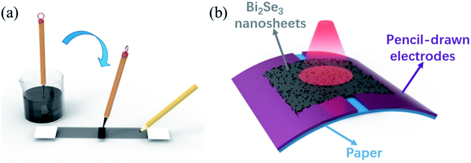 | ||
| Fig. 1 (a) Schematic diagram of the device of the fabrication procedure for direct writing using a pencil and Chinese brush on paper. (b) Schematic diagram of the flexible device structure. | ||
2.3 Characterization
The surface morphologies of the samples were characterized by scanning electron microscopy (SEM, Tescan Vega 3 SBH) and using a digital camera. Raman spectra of the as-prepared Bi2Se3 nanosheets were acquired by employing a Renishaw InVia Raman microscope (excitation wavelength 532 nm). Optoelectronic measurements were carried out via a semiconductor characterization system (Keithley 2612B) and the power value of the light source (1064 nm) was confirmed with an optical power meter (PM100D Thorlabs).3. Results and discussion
The schematic structure of the flexible photodetector device based on Bi2Se3 nanosheets is exhibited in Fig. 1(b). It can be noted that the electrodes are drawn evenly in pencil and its functional material is graphite. Graphite with high charge carrier mobility is composed of 2D graphene sheets,33 addressing the needs of high conductivity as well as flexibility for a flexible device. In contrast to other substrates, common paper with flexibility was chosen as the substrate as it possessed unique advantages; it can be tailored to any size and shape,34 endowing it with unprecedented attractiveness for flexible device applications. Bi2Se3 nanosheets were selected as the light-sensitive material due to their intrinsic superior optoelectronic properties and high durability. Fig. 2(a) shows the schematic diagram of the flexible device based on graphite electrodes; a 1064 nm laser was used as the excitation light source. The inset of Fig. 2(a) exhibits the digital photograph of the real device based on pencil-drawn electrodes. Fig. 2(b) shows the typical X-ray diffraction (XRD) spectra of as-prepared Bi2Se3 nanosheets. The diffraction peaks at 18.4°, 24.9°, 27.7°, 29.4°, 35.3°, 40.4°, 43°, 43.6° and 47.6° observed in the XRD patterns can be indexed to the (006), (101), (104), (015), (018), (10 10), (01 11), (110) and (00 15) crystal planes, in accordance with Bi2Se3 nanosheets (JCPDS card no. 12-0732). All the diffraction peaks are indexed to Bi2Se3 without other impurities, suggesting that the sample possesses high purity and good crystallinity. In order to further confirm the composition of the sample, Raman spectroscopy (excited with a 532 nm laser) was carried out and it exhibits the existence of a characteristic peak of Bi2Se3 in Fig. 2(c). The Raman peak observed at 130 cm−1 can be attributed to the in-plane E2g mode, and peaks at 71 cm−1 and 173 cm−1 correspond to the A11g and A21g vibration modes of Bi2Se3,35,36 respectively. There are no other characteristic peaks in the above results, which strongly demonstrates that pure Bi2Se3 nanosheets have been successfully synthesized by liquid exfoliation. Further SEM investigation (Fig. 2(d)) depicts a uniform and stacked distribution of Bi2Se3 nanosheets, which is proposed to be helpful to form a steady dense film for the transport of photogenerated charge carriers.29 The high magnification SEM image shown in the inset of Fig. 2(d) reveals that as-exfoliated Bi2Se3 nanosheets have lateral dimensions of 2 μm. As shown in Fig. 2(e), the electrodes are composed of a uniform and dense graphite film on paper, which are proposed as a highway to boost the movement of photogenerated charge carriers.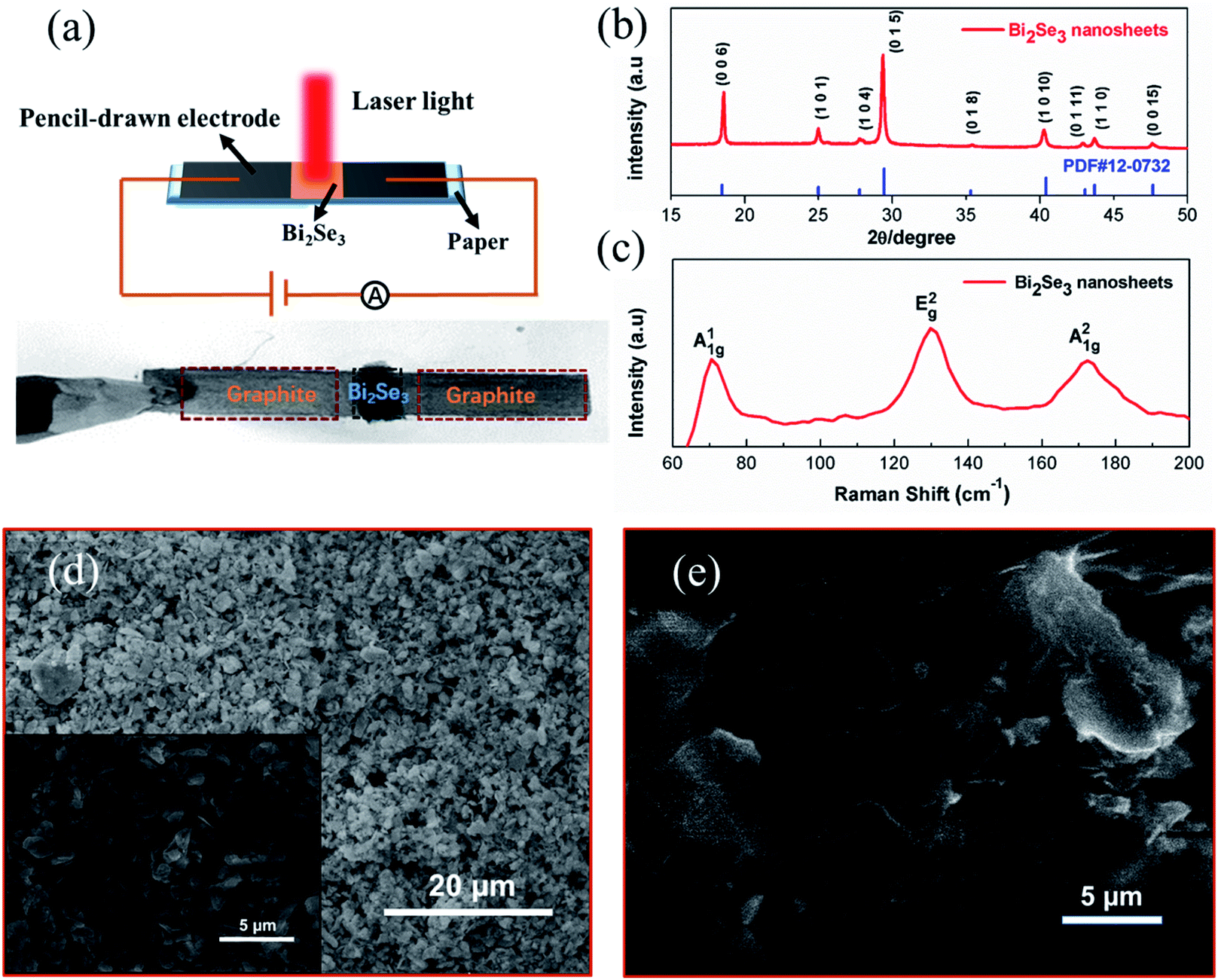 | ||
| Fig. 2 (a) Schematic diagram of the experimental setup, inset: digital photograph of the real device. (b) XRD spectra of the Bi2Se3 nanosheets. (c) Raman spectrum of Bi2Se3 nanosheets. (d) Low-magnification SEM images of the liquid-exfoliated Bi2Se3 nanosheets, inset: high-magnification SEM images of the liquid-exfoliated Bi2Se3 nanosheets. (e) SEM images of pencil-drawn electrodes. | ||
Fig. 3 demonstrates the optoelectronic performances of a photoconductive photodetector under 1064 nm laser illumination. It is obvious that the as-prepared device presents excellent photoresponse characteristics. The linear current–voltage (I–V) curves, as shown in Fig. 3(a), imply that there is good ohmic contact between 2D Bi2Se3 and the graphite electrode, which is considered to benefit the extraction of photogenerated charge carriers.29 The inset of Fig. 3(a) shows that the electrons of Bi2Se3 move from the valence band to the conduction band via the infrared light excitation. Subsequently, with the help of the applied electric field, the photogenerated electron–hole pairs are quickly separated and transported through graphite electrodes.37 Thus, the pencil-drawn device can work effectively. The photocurrent switching characteristics of the pencil-drawn photodetector were further evaluated. As shown in Fig. 3(b), the temporal photoresponse of the photodetector was recorded by manually keeping out the light source every 20 seconds at 5 V bias voltage, and it was found that the electrical conductivity of the photodetector was affected by the light illumination. Under light irradiation conditions, the photocurrent rises immediately, and drops sharply when it is sheltered. Consistently, it can be seen that the photocurrent is closely related to the light intensity and monotonously increases with the change of light intensity from 3.16 mW mm−2 to 10.65 mW mm−2, which results from the increase in the number of non-equilibrium carriers with the increase of light intensity. Meanwhile, the steady photocurrent is about 0.35 μA when the light intensity is 3.76 mW mm−2, demonstrating that our device possesses high infrared response characteristics. In addition, we examined the photocurrent of the pencil-drawn device by applying different bias voltages varied from 1 to 5 V as shown in Fig. 3(c). Notably, the photocurrent of the device is related to the applied bias, where the photocurrent reached by the device is about 0.15 μA at a bias of 1 V and gradually ascends to 0.82 μA when the bias increased to 5 V. These phenomena indicate that we can adjust the photoresponse of the device by finding an optimal bias voltage. It is well known that responsivity is a critical factor to evaluate the performance of photodetectors, which can be acquired through the following formula: R = I/Jlight, in which I is the photocurrent and Jlight is the irradiance intensity. The dependence of responsivity on irradiance power intensity is demonstrated in Fig. 3(d). Noticeably, the responsivity basically does not vary as the light intensity changes from 2 mW mm−2 to 10.65 mW mm−2 and the responsivity undergoes a very slight decrease owing to the recombination of electron–hole pairs when light intensity rises over 5.46 mW mm−2. The outstanding photocurrent density and high responsivity of Bi2Se3 nanosheets suggest a good prospect for their practical application in infrared photodetectors. Apart from the photoelectric responsivity, the stability of the photodetector is another critical factor that should be evaluated before its practical application. Herein, cycle stability measurement has been conducted and is shown in Fig. 3(e) to evaluate the robustness of the device. It is apparent that the photocurrent displays negligible decay after successive switching operation for 800 s, revealing that the pencil-drawn device is highly stable and can maintain good reproducibility.
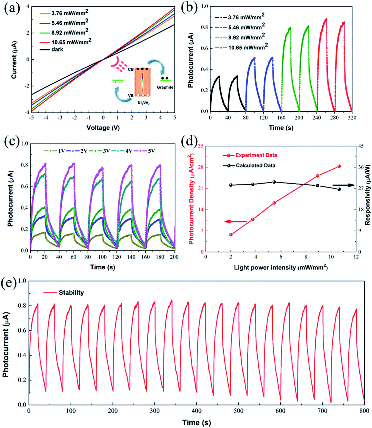 | ||
| Fig. 3 (a) I–V characteristics of the device under dark and various light intensities, inset: the working principle of the photodetector. (b) I–t curves at 5 V of the device under 1064 nm irradiation with different light intensities. (c) I–t curves at 10.65 mW mm−2 of the device under different voltages (1–5 V). (d) Fitting curve and calculated responsivity of the device under various light intensities (e) cycling stability measurement of the device. | ||
Another merit of the device is its flexibility. As described above, all the components of the as-fabricated device (active material, electrode, and substrate) are flexible enough to support the mechanically foldable device. The photocurrents of the device with various bending curvatures under 1064 nm light irradiation are shown in Fig. 4(a). The insets showing real photographs of the device in Fig. 4(a) correspond to the device being bent at 60°, 100°, 130°, 140° and 160°, respectively, indicating that the device possesses high flexibility and conductivity. In addition, in order to more intuitively understand the relationship between the bending angle and the photocurrent of the device, fitting curves of the photocurrent of the flexible photodetector under different bending angles were obtained and are depicted in Fig. 4(b). Notably, the photocurrent gradually decreases as the bending angle of the device increases and returns to the pristine level when the device was restored. The slight photocurrent decrease during bending may be related to the less active area under the deflected conditions, because the radius of the light spot is only about 1 mm, the area of illumination changes under bending conditions, resulting in changes of the photocurrent. Moreover, the photocurrent of the device is recorded in Fig. 4(c) after multiple bending cycles. Encouragingly, the photocurrent barely changed after being bent for 0, 100, 200, 400 and 1000 cycles except for a little fluctuation noise, powerfully demonstrating that the device has excellent electrical stability and long-term flexibility. Fig. 4(d) shows the time-dependent photocurrent (I–t) curves of the pencil-drawn device after the 1st and 1000th bending–recovery cycle. The photocurrent of the device is about 42 nA after bending 1000 times and the pristine photocurrent before bending is 44 nA, suggesting that the device has good stability and fluctuations are less than 5%. Noticeably, our device still maintains excellent switching performance after bending for 1000 cycles. These results indicate that the pencil-drawn device has high flexibility, stability and durability in the bending state.
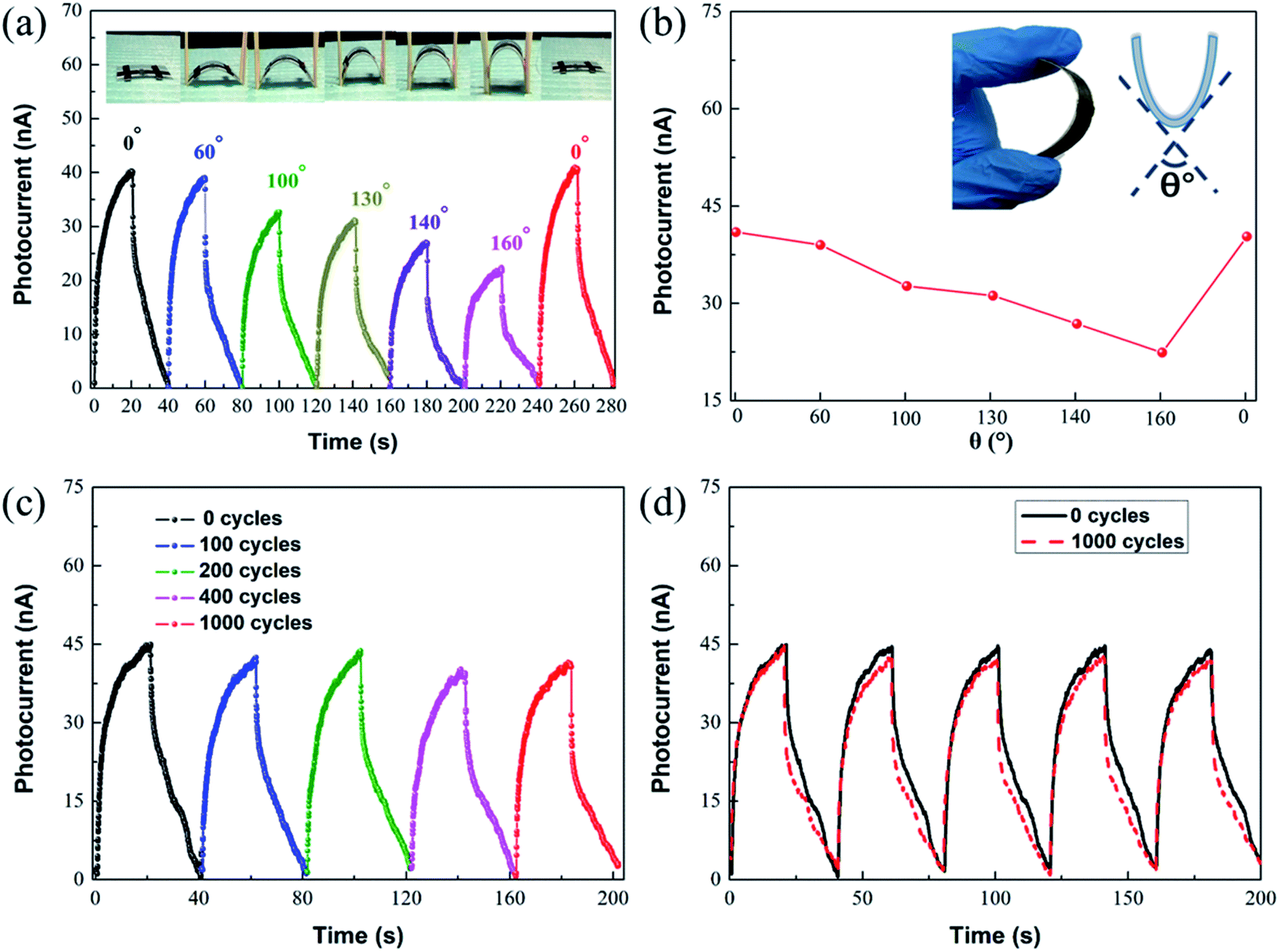 | ||
| Fig. 4 (a) I–t curves with an applied voltage of 5 V of the flexible photodetector under various power intensities, the insets show the corresponding photographs of the device under different bending angles. (b) Photocurrent fitting curve of the flexible photodetector under different bending angles. (c) I–t curves of the flexible photodetector after 0 bending cycles, 100 bending cycles, 200 bending cycles, 400 bending cycles and 1000 bending cycles. (d) I–t curves of the flexible photodetector after the 1st and 1000th bending–recovery cycle. | ||
4. Conclusions
In summary, we have designed and fabricated a novel flexible infrared photodetector with decent performances. Liquid-exfoliated Bi2Se3 nanosheets were adopted as the light absorbing material, and pencil-drawn graphite was employed as the electrode on a common paper substrate. 2D Bi2Se3 nanosheets were synthesized via a facile liquid exfoliation method and its particular properties are suitable for portable and wearable optoelectronic devices. The as-fabricated flexible photodetector exhibits both superior photocurrent and high responsivity to infrared light (1064 nm). Impressively, the pencil-drawn flexible photodetector displays functionality and long-term durability under bending conditions, demonstrating promising prospects for wearable and flexible optoelectronic applications. All the results will contribute to the development of photodetectors for cost-efficient, flexible and infrared light detection.Conflicts of interest
There are no conflicts of interest to declare.Acknowledgements
This work was supported by Grants from the National Natural Science Foundation of China (No. 11504312, 51772255), Scientific Research Fund of Hunan Provincial Education Department (No. 18A059), Open Fund based on Innovation Platform of Hunan Colleges and Universities (No. 18K032), Provincial Natural Science Foundation of Hunan (No. 2019JJ50612), the Program for Chang Jiang Scholars and Innovative Research Team in University (IRT_17R91) and Science and Technology Program of Xiangtan (No. CXY-ZD20172002).References
- S. Ohta, H. Nakamoto, Y. Shinagawa and T. Tanikawa, J. Telemed. Telecare, 2002, 8, 151–156 CrossRef PubMed.
- P.-S. Murvay and I. Silea, J. Loss Prev. Process. Ind., 2012, 25, 966–973 CrossRef CAS.
- M. Sundaram, S. C. Wang, M. F. Taylor, A. Reisinger, G. L. Milne, K. B. Reiff, R. E. Rose and R. R. Martin, Infrared Phys. Technol., 2001, 42, 301–308 CrossRef.
- Z. Cui, F. R. Poblete, G. Cheng, S. Yao, X. Jiang and Y. Zhu, J. Mater. Res., 2014, 30, 79–85 CrossRef.
- Q. Bao and K. P. Loh, ACS Nano, 2012, 6, 3677–3694 CrossRef CAS PubMed.
- R. Cao, H. D. Wang, Z. N. Guo, D. K. Sang, L. Y. Zhang, Q. L. Xiao, Y. P. Zhang, D. Y. Fan, J. Q. Li and H. Zhang, Adv. Opt. Mater., 2019, 1900020 CrossRef.
- J. Song, J. Yuan, F. Xia, J. Liu, Y. Zhang, Y. L. Zhong, J. Zheng, Y. Liu, S. Li and M. Zhao, Adv. Electron. Mater., 2016, 2, 1600077 CrossRef.
- M. K. Jana, P. Chithaiah, B. Murali, S. Krupanidhi, K. Biswas and C. Rao, J. Mater. Chem. C, 2013, 1, 6184–6187 RSC.
- W. Yu, S. Li, Y. Zhang, W. Ma, T. Sun, J. Yuan, K. Fu and Q. Bao, Small, 2017, 13, 1700268 CrossRef PubMed.
- F. Koppens, T. Mueller, P. Avouris, A. Ferrari, M. Vitiello and M. Polini, Nat. Nanotechnol., 2014, 9, 780 CrossRef CAS PubMed.
- J. Chao, S. Xing, Z. Liu, X. Zhang, Y. Zhao, L. Zhao and Q. Fan, Mater. Res. Bull., 2018, 98, 194–199 CrossRef CAS.
- B. Chitara, L. Panchakarla, S. Krupanidhi and C. Rao, Adv. Mater., 2011, 23, 5419–5424 CrossRef CAS PubMed.
- X. Ren, Z. Li, Z. Huang, D. Sang, H. Qiao, X. Qi, J. Li, J. Zhong and H. Zhang, Adv. Funct. Mater., 2017, 27, 1606834 CrossRef.
- A. Castellanos-Gomez, L. Vicarelli, E. Prada, J. O. Island, K. Narasimha-Acharya, S. I. Blanter, D. J. Groenendijk, M. Buscema, G. A. Steele and J. Alvarez, 2D Mater, 2014, 1, 025001 CrossRef.
- W. Choi, N. Choudhary, G. H. Han, J. Park, D. Akinwande and Y. H. Lee, Mater. Today, 2017, 20, 116–130 CrossRef CAS.
- D. J. Late, B. Liu, H. R. Matte, V. P. Dravid and C. Rao, ACS Nano, 2012, 6, 5635–5641 CrossRef CAS PubMed.
- Y. Chen, G. Jiang, S. Chen, Z. Guo, X. Yu, C. Zhao, H. Zhang, Q. Bao, S. Wen and D. Tang, Opt. Express, 2015, 23, 12823–12833 CrossRef CAS PubMed.
- V. Goyal, D. Teweldebrhan and A. A. Balandin, Appl. Phys. Lett., 2010, 97, 133117 CrossRef.
- C. Kane and M. Hasan, Rev. Mod. Phys., 2010, 82, 3045–3067 CrossRef.
- Y. Chen, J. G. Analytis, J.-H. Chu, Z. Liu, S.-K. Mo, X.-L. Qi, H. Zhang, D. Lu, X. Dai and Z. Fang, Science, 2009, 325, 178–181 CrossRef CAS PubMed.
- A. Sharma, B. Bhattacharyya, A. Srivastava, T. Senguttuvan and S. Husale, Sci. Rep., 2016, 6, 19138 CrossRef CAS PubMed.
- H. Peng, W. Dang, J. Cao, Y. Chen, D. Wu, W. Zheng, H. Li, Z.-X. Shen and Z. Liu, Nat. Chem., 2012, 4, 281 CrossRef CAS PubMed.
- H. Zhu, C. A. Richter, E. Zhao, J. E. Bonevich, W. A. Kimes, H.-J. Jang, H. Yuan, H. Li, A. Arab and O. Kirillov, Sci. Rep., 2013, 3, 1757 CrossRef.
- H. Zhang, C.-X. Liu, X.-L. Qi, X. Dai, Z. Fang and S.-C. Zhang, Nat. Phys., 2009, 5, 438 Search PubMed.
- L. Sun, Z. Lin, J. Peng, J. Weng, Y. Huang and Z. Luo, Sci. Rep., 2014, 4, 4794 Search PubMed.
- M. Z. Hossain, S. L. Rumyantsev, K. M. Shahil, D. Teweldebrhan, M. Shur and A. A. Balandin, ACS Nano, 2011, 5, 2N57–2663 Search PubMed.
- F. Wang, L. Li, W. Huang, L. Li, B. Jin, H. Li and T. Zhai, Adv. Funct. Mater., 2018, 28, 1802707 CrossRef.
- H. Zhang, X. Zhang, C. Liu, S.-T. Lee and J. Jie, ACS Nano, 2016, 10, 5113–5122 CrossRef CAS PubMed.
- F. Cao, D. Yu, X. Li, Y. Zhu, Z. Sun, Y. Shen, Y. Wu, Y. Wei and H. Zeng, J. Mater. Chem. C, 2017, 5, 7441–7445 RSC.
- Y. Zhang, Z. Duan, H. Zou and M. Ma, Sens. Actuators, B, 2018, 261, 345–353 CrossRef CAS.
- N. Dossi, R. Toniolo, A. Pizzariello, F. Impellizzieri, E. Piccin and G. Bontempelli, Electrophoresis, 2013, 34, 2085–2091 CrossRef CAS PubMed.
- Z. Li, H. Qiao, Z. Guo, X. Ren, Z. Huang, X. Qi, S. C. Dhanabalan, J. S. Ponraj, D. Zhang and J. Li, Adv. Funct. Mater., 2018, 28, 1705237 CrossRef.
- K. S. Novoselov, A. K. Geim, S. V. Morozov, D. Jiang, Y. Zhang, S. V. Dubonos, I. V. Grigorieva and A. A. Firsov, Science, 2004, 306, 666–669 CrossRef CAS PubMed.
- L. Yang, A. Rida, R. Vyas and M. M. Tentzeris, IEEE Trans. Microwave Theory Tech., 2007, 55, 2894–2901 Search PubMed.
- X. Chen, H. Tang, Z. Huang, J. Zhou, X. Ren, K. Huang, X. Qi and J. Zhong, Ceram. Int., 2017, 43, 1437–1442 CrossRef CAS.
- J. Zhang, Z. Peng, A. Soni, Y. Zhao, Y. Xiong, B. Peng, J. Wang, M. S. Dresselhaus and Q. Xiong, Nano Lett., 2011, 11, 2407–2414 CrossRef CAS PubMed.
- J. Song, L. Xu, J. Li, J. Xue, Y. Dong, X. Li and H. Zeng, Adv. Mater., 2016, 28, 4861–4869 CrossRef CAS PubMed.
- Z. Xie, C. Xing, W. Huang, T. Fan, Z. Li, J. Zhao, Y. Xiang, Z. Guo, J. Li and Z. Yang, Adv. Funct. Mater., 2018, 28, 1705833 CrossRef.
- C. Xing, W. Huang, Z. Xie, J. Zhao, D. Ma, T. Fan, W. Liang, Y. Ge, B. Dong and J. Li, ACS Photonics, 2017, 5, 621–629 CrossRef.
- W. Huang, C. Xing, Y. Wang, Z. Li, L. Wu, D. Ma, X. Dai, Y. Xiang, J. Li and D. Fan, Nanoscale, 2018, 10, 2404–2412 RSC.
- C. Zang, X. Qi, L. Ren, G. Hao, Y. Liu, J. Li and J. Zhong, Appl. Surf. Sci., 2014, 316, 341–347 CrossRef CAS.
| This journal is © The Royal Society of Chemistry 2020 |