
 Open Access Article
 This Open Access Article is licensed under a Creative Commons Attribution-Non Commercial 3.0 Unported Licence
Femtosecond laser-induced non-thermal welding for a single Cu nanowire glucose sensor†
Yongchao
Yu
 a,
Yangbao
Deng
b,
Md Abdullah
Al Hasan
a,
Yanfeng
Bai
ac,
Ruo-Zhou
Li
d,
Shuguang
Deng
b,
Pooran
Joshi
e,
Seungha
Shin
*a and
Anming
Hu
*a
a,
Yangbao
Deng
b,
Md Abdullah
Al Hasan
a,
Yanfeng
Bai
ac,
Ruo-Zhou
Li
d,
Shuguang
Deng
b,
Pooran
Joshi
e,
Seungha
Shin
*a and
Anming
Hu
*a
aDepartment of Mechanical, Aerospace and Biomedical Engineering, University of Tennessee Knoxville, 1512 Middle Drive, Knoxville, TN 37996, USA. E-mail: ahu3@utk.edu; sshin@utk.edu
bAll-solid-state Energy Storage Materials and Devices Key Laboratory of Hunan Province, College of Information and Electronic Engineering, Hunan City University, Yiyang 413000, P. R. China
cCollege of Computer Science and Electronic Engineering, Hunan University, Changsha 410082, P. R. China
dCollege of Electronic and Optical Engineering & College Microelectronics, Nanjing University of Post and Telecommunications, Nanjing 210023, P. R. China
eOak Ridge National Laboratory, 1 Bethel Valley Rd, Oak Ridge, TN 37830, USA
First published on 23rd January 2020
Abstract
Copper nanowires (CuNWs) are a key building block to facilitate carrier conduction across a broad range of nanodevices. For integration into nanoscale devices, manipulation and welding of these nanowires need to be overcome. Based on high energy density laser processing investigation, we report on innovative welding of single CuNWs to a silver film using a tightly focused laser beam combined with manipulation of CuNWs through the dielectrophoresis (DEP) method. Two types of lasers, femtosecond (FS) and continuous-wave (CW), were employed to analyze, improve, and control Cu-NW melting characteristics under high energy density irradiation. The FS laser welding of CuNWs resulted in a metallic joint with a low contact resistance suitable for functional electronic nanodevices. Computational simulations using the 1-D heat diffusion equation and finite difference method (FDM) were performed to gain an insight into metal–laser interactions for high performance welded contact development. Simulation studies on lasers established contrasting melting behavior of metal under laser irradiation. The device feasibility of CuNW based welded contacts was evaluated in terms of the electrical performance of a glucose sensor. It was possible to sense glucose concentration down to 10−6 M, demonstrating a path towards integration of CuNWs into wearable, flexible nanoelectronic devices.
1. Introduction
Nanoelectronics is rapidly evolving towards multi-functional, high reliability, and high integration density systems through 1D–3D integration of materials, process technology, and packaging. Among the nanotechnology-enabled materials, metallic and semiconducting nanowires have been pursued as key building blocks to manufacture a broad range of nanodevices, e.g., single-photon detectors,1 transparent and flexible electrodes,2–4 organic electronic and heat-sensitive functional devices,5 electrical and thermal conduction devices,6 foldable capacitive touch pads,7 stretchable and wearable electronics,8–10 and sensors.11–13 Specifically, single-nanowire devices with unique nanostructures and properties become attractive and promising for diverse applications. However, to realize large-scale, reliable manufacture of single nanowire devices, the following two technical barriers must be overcome: nano-manipulation and nano-welding.Nano-manipulation to enable controlled assembly of nanoscale building blocks is essential for nanomanufacturing. To fabricate single nanowire devices, several methods have been established for manipulating NWs, including electric field-assisted alignment,14–17 flow-assisted alignment,18 the blow bubble method,19 contact printing,20 direct growth of NW devices,21 the Langmuir–Blodgett technique,22 optical tweezers,23,24 optoelectrical tweezers25 and micro-robots.26,27 Compared with other methods, the electric field-assisted alignment28 has been widely applied to control different types of NWs, such as semiconductors, metals, and carbon, normally by dielectrophoresis (DEP) force. DEP exerts a force on dielectric NWs through induced dipoles when NWs are subjected to a non-uniform electric field. NWs are polarized and aligned with a minimum energy configuration within an applied electric field, which is along the electric field lines. The electric field-assisted alignment is affected by many factors including the suspending medium, the relative dielectric constant (defined as the ratio of the permittivity of a substance to that of free space) and the geometry of NWs.29
Welding of NWs can provide an opportunity and potential to form lots of functional nanoelectronics,30 including nanocircuits,31 light-gated nanowire transistors,32 nano-waveguides and nanophotonic circuits for quantum computation,33,34 and nanoplasmonic devices.35 To realize a nanoscale joining, various methods have been proposed and applied to join NWs, such as cold-welding,36–38 Joule heating,39–42 thermal annealing,43 mechanical pressure,44 and laser (laser-induced plasmonic) joining.45–51 Solid-state diffusion driven by surface energy has enabled welding of two bare Au NWs in a vacuum at room temperature36 and joining of two silver NWs after the removal of the surface-capping polymer in an ambient atmosphere.37,38 However, it is difficult to achieve a head-to-side joining (T-shape) through this self-diffusion since the capping layer is not uniform, and the polymer at the sidewall is thicker than the layer at the wire head.37 Although Joule heating was suggested to join NWs,39,40 it is limited to conductive NWs. A nanoscopic mechanical press with nanoindentation was developed to join a wire to a substrate.44 Unfortunately, this press will significantly deform the wire head. The substrate can be damaged seriously by Joule heating, mechanical pressure and thermal annealing unless the processing parameters, e.g., current, pressure, and temperature, are accurately controlled. Compared with other joining methods, photonic sintering was conducted for joining metal NWs, which can provide non-contact processing and good thermal controllability with minimum thermal damage to the substrate. Due to self-localized plasmonic excitation,45 this plasmonic heat can lead to perfect joining at cross-overlapped NWs.7 A continuous-wave laser was employed to melt part of NWs for brazing the crossed NWs.47,52 This laser nanobrazing is similar to autogenous laser brazing developed for metal microjoining.53 Currently, laser joined metal NWs display a polycrystalline nature with lots of defects in the joined regions.49,50,54 This is quite different from self-oriented joining with solid-state diffusion where a clear lattice matching is founded. Femtosecond laser joining and laser-healing of cutting wires show epitaxial recrystallization or enhanced grain orientation.50,54,55 Therefore, the nanojoining quality can be feasibly improved through precise control of laser parameters based on the understanding of the interaction of the laser and NWs.
In this work, for a better understanding of the local melting of a CuNW using a focused laser beam, a comparative study is accomplished with a 1030 nm FS laser and 532 nm continuous-wave (CW) laser under different power and atmosphere conditions. To support the experimental observation and explain the difference between the two types of laser irradiation, we conducted computational modeling of the temperature distribution of CuNWs. For the simulation, we model CuNWs as a circular rod with a length of 30 μm and a diameter of 200 nm and assume that the laser is irradiated at the tip of a modeled NW, and the temperature is distributed only along the length (defined as the x direction) as shown in Fig. S5.† Therefore, a one-dimensional (1-D) heat diffusion model and the finite difference method are employed for the thermal analysis of both types of laser irradiation. In the case of the CW laser, assuming a steady heat supply, a single-temperature model is used to calculate the temperature distribution and its evolution. In contrast, simulations of FS laser irradiation consider the electron and lattice temperatures (Te and Tl), separately (i.e., a two-temperature model) due to the time-dependent heat flow from electrons to the lattice. This time dependence is because the electron excitation by the laser (interaction time: ∼a few fs (ref. 56)) is much faster than the electron–phonon interaction (∼1 ps) and the pulse duration (300 fs) is too short for electrons to excite any ions thermally.57,58
As an application, a single copper nanowire (CuNW) device has been fabricated at room temperature with a regular air environment with a 1030 nm FS laser as a glucose sensor. A single CuNW glucose sensor on a flexible paper substrate was successfully demonstrated with a detection limit of about 10−6 M.
2. Results and discussion
In this study, CuNWs were synthesized by a hydrothermal method. Fig. S1(a)–(c) (see the ESI†) show the SEM images for the synthesized CuNWs. The self-joined phenomenon was observed between CuNWs, which is due to the inhomogeneous removal of surface capping layers. In Fig. S1(c),† two CuNWs are head-to-head joined and form an angle of 132°. An organic compound, octadecylamine (ODA), was used for the synthesis of CuNWs. To remove ODA from CuNW solution, the CuNW solution was washed with ethanol 2–4 times. It is found that ODA films at the end of CuNWs were thinner than the sidewall. The diffusion between two adjacently exposed wires leads to an end-to-end joining. The average length of CuNWs is around 28.4 μm, with 250–350 nm diameter. Fig. S1(f)† shows the statistic distribution of the joined angles. The dominant angles are mainly distributed in a range of 110–160°. Although this self-joined nanowire has been selectively applied for simple plasmonic circuits through lithographic manufacturing, this joined wire is not suitable for complicated nanoelectronics with the desired function. Fig. S1(g)† shows the X-ray diffraction (XRD) pattern of CuNWs. The diffraction peaks are located at the values of 43.45° and 50.6°, which match with (111) and (200) planes.59 There is no diffraction peak of CuO or any other compound observed from the XRD result, which suggests the high purity of the as-prepared face-centered cubic crystal structured CuNWs.In order to elucidate the laser-induced melting of a Cu nanowire, two types of lasers (1030 nm femtosecond (FS) laser and 532 nm continue wave (CW) green laser) have been compared. Fig. 1 shows the SEM images of laser irradiated CuNWs. The experiments were performed at room temperature and in an ambient atmosphere. The laser beam was focused by a long working distance 100× microscope lens with an NA of 0.8. After focusing, the diameter of the laser beam spot applied to the substrate was around 1 μm. Fig. 1(a)–(c) show the experimental results for the FS laser with an average laser power of 35 mW and Fig. 1(d)–(f) show the experimental results for the CW laser at the same average power of 35 mW. Obviously, under the same laser power conditions, the two laser irradiations create significant differences. For the FS laser, explosive deformations can be observed on both the substrate and CuNW after the laser process (Fig. 1(b) and (c) compared with Fig. 1(a)). The silicon wafer substrate is damaged, and a large number of Si and Ag nanoparticles splash around in the irradiation area. A large particle aggregation appears on top of the NW. However, there is no structural and surface deformation on other parts of the nanowire. On the other hand, under the same laser power conditions, the CW laser produced a different effect from that with the FS laser. Comparing Fig. 1(e) to (d), it is found that the CW laser does not break a CuNW at all but causes a very clear surface deformation on the nanowire. As shown in Fig. 1(f), at the laser-focused position, the CuNW is partially melted at high temperatures induced by CW laser irradiation, and then the melted wire solidifies and crystallizes again after the laser is turned off. Furthermore, this thermal effect is propagated along the CuNW, and causes an increase of the surface roughness of the entire nanowire. As demonstrated in Fig. S2(a) and (b),† the surface of the un-irradiated area is kept clean and smooth before and after FS laser irradiation. However, after CW laser irradiation, a clear surface change can be observed even in the un-irradiated area (Fig. S2(c) and (d)†). Because the CuNW was exposed to air, serious oxidation could occur on the surface due to the heat induced by the CW laser, which will be further confirmed by chemical analysis later. The FS laser is an ultra-fast high repetition pulse laser, with an average laser power of 35 mW, and it can generate a peak power density of 1.24 × 10¹⁴ W cm−2. On the other hand, with 35 mW power, the CW laser generates a power density of 4.46 × 10⁶ W cm−2. Meanwhile, for an ultrafast interaction, the absorption of photons stimulates electrons within a hundred femtoseconds (fs), which is too short to disturb the lattice. The absorbed energy was thus transferred from electrons to the lattice by electron–lattice scattering after the laser pulse irradiation.58,60 The thermal coupling between free electrons and lattices typically occurs within 100 ps, depending on the electron–phonon coupling strength of different materials. The typical electron–phonon coupling time of hundred femtoseconds is much shorter than the heat transfer period by thermal conduction. Therefore, the thermal diffusion to the laser-irradiated surrounding area is very limited.61
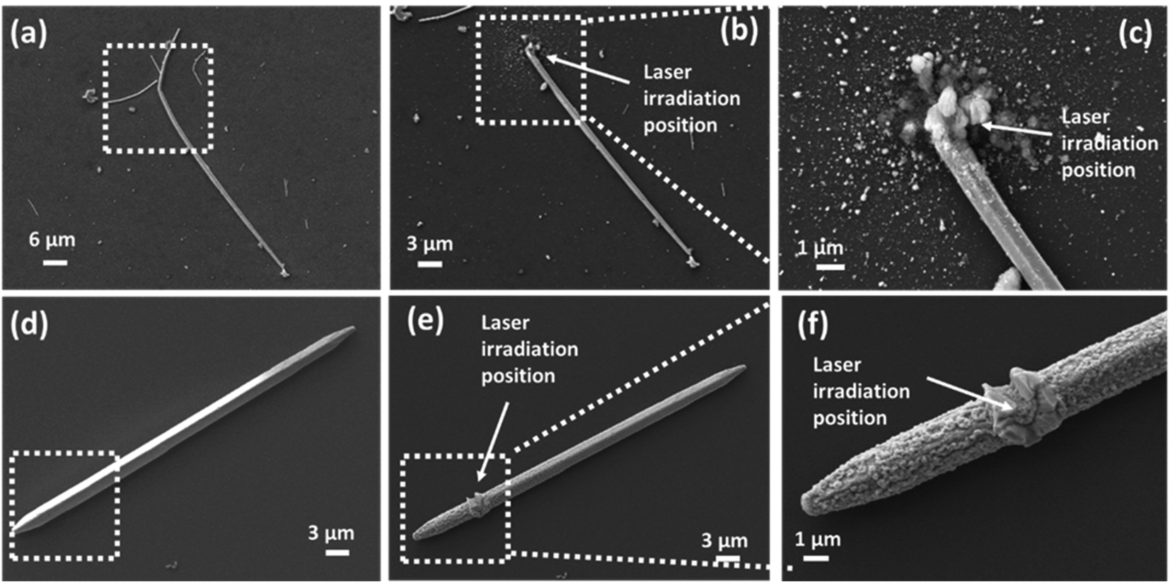 | ||
| Fig. 1 SEM images of a CuNW (a) before and (b) after FS laser irradiation and (c) enlarged image of the FS laser irradiation area. CuNW images (d) before and (e) after CW laser irradiation and (f) enlarged image of the CW laser irradiation area. | ||
To elucidate the origin of the surface deformation on the CuNW, energy dispersive X-ray spectroscopy (EDS) analyses were conducted through elemental mapping. Fig. 2(a) and (b) show the EDS results of CuNWs irradiated with the CW laser and FS laser in an ambient atmosphere. Fig. 2(a) shows a clear oxygen response on the surface of the CuNW after the CW irradiation, specially in the recrystallized area marked with a white arrow. This indicates surface oxidization induced by laser irradiation. In contrast, as shown in Fig. 2(b), the oxygen response on the CuNW surface irradiated with the FS laser is within the detection error of EDS analyses under the same conditions. These results infer that the surface structural change is introduced by the oxidation of Cu, which is caused by local, high temperature induced by the laser and oxygen in the air. To further verify this, the same experiments were carried out in a glove box with Ar buffer gas and both oxygen and water concentrations were lower than 0.1 ppm. Experiment results and EDS analysis results are shown in Fig. 2(c) and (d). From Fig. 2(c), we observed that at the end of the nanowire, where the CW laser is irradiated, there is a critical indication of melting. The shape and surface changes of the CuNW (from a pentagon to a round shape with a smooth surface) can be observed.
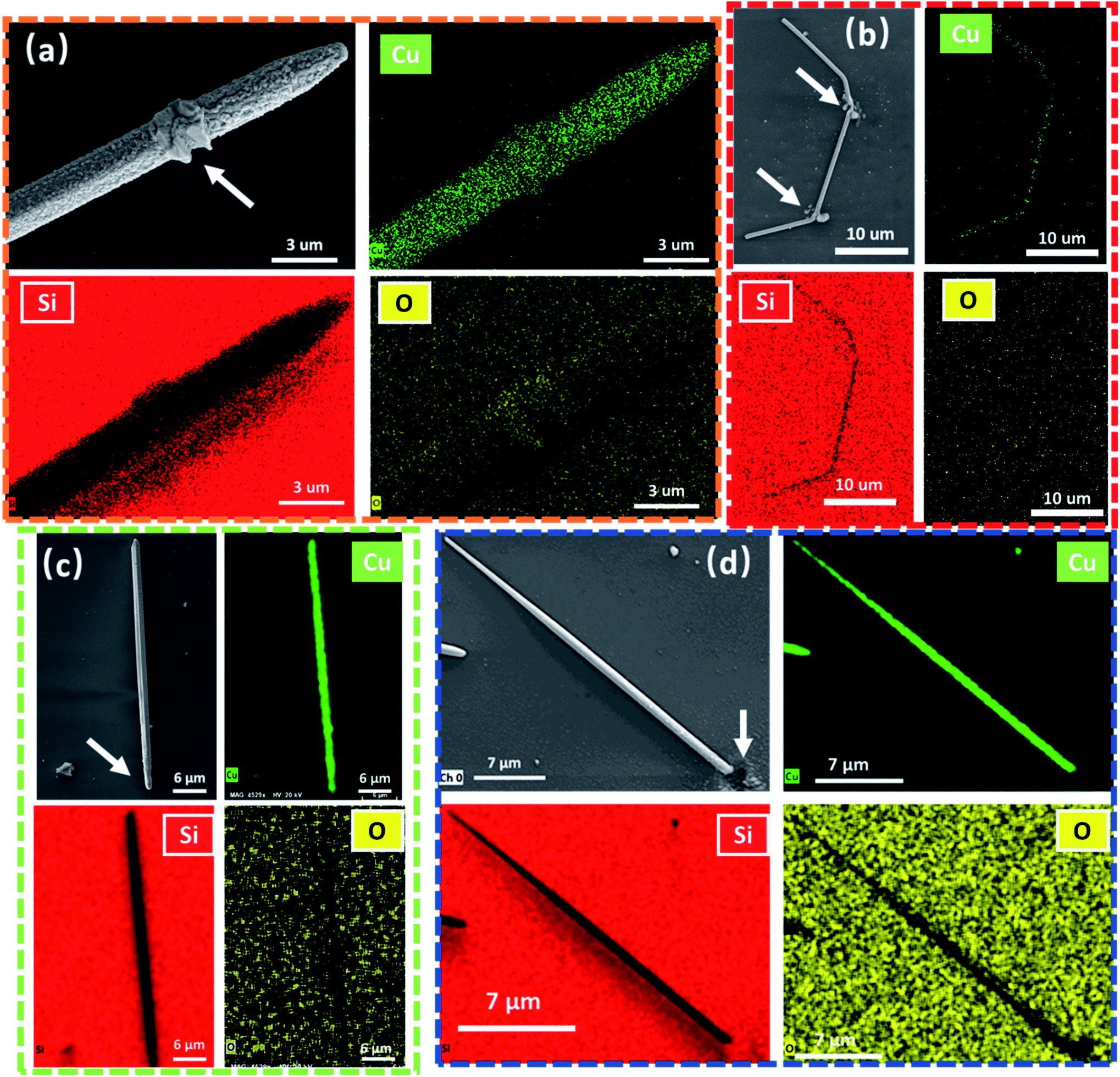 | ||
| Fig. 2 EDS mapping results for the (a) CW laser processed sample in air, (b) FS laser processed sample in air, (c) CW laser processed sample in Ar, and (d) FS laser processed sample in Ar. | ||
Different from Fig. 2(a), other nanowires irradiated by the FS laser and CW laser operating in a protective gas do not display surface roughness change; i.e., the nanowire surface remains smooth and clean. The EDS analysis also shows no remarkable change in the oxygen element distribution. Additionally, for the FS laser sample, no discernible difference has been detected between two different environmental conditions. Both samples that were processed under air and Ar conditions present very similar results, explosive deformation at laser irradiation positions, and a clean and smooth surface in the entire unaffected area. At this point, it can be concluded that the surface deformation of the CuNW processed with the CW laser is due to oxidization. The CW laser induces significant thermal diffusion, which leads to oxidization on the entire nanowire. In contrast, the diffusion of the thermal effect induced by the FS laser to the non-irradiation area is minimized. The dynamic procedures of these experimental results are further investigated by computational simulation. These results not only evidence the FS laser as an ideal tool for precise processes but also show the advantage of the FS laser to process an easily oxidized material in air.
On this basis, studies on the effects of the laser power of the FS laser and the CW laser were accomplished. For the FS laser, it is clear that explosive deformations will occur at an average laser power of 35 mW. Thus the laser power has to be reduced to avoid damage to the NWs and Si substrate. Ultimately, the laser power was decreased from 35 mW to 4 mW. Laser powers of 5 mW and 4 mW were also used to determine the minimum laser processing power. For the CW laser, the experiment shows that with 35 mW laser power irradiation, the laser only melts a limited area of the CW surface. From the point of laser microprocessing, such limited surface melting cannot provide enough contribution to the nano-welding or nano-joining process. For a better understanding of CW laser effects on CuNWs, the laser power was increased from 35 mW to 45 mW. All the experiments were performed in a glove box to protect CuNWs from oxidization. Fig. S3(a)–(c)† show the SEM images of CuNWs after being processed with the FS laser with different laser powers. From the images, as the laser power decreased from 10 mW to 4 mW, the size of holes induced by laser ablation on the substrate was reduced from about 4 μm to about 2.5 μm. It is worth noting that at 5 mW laser power, the agglomeration of large particles did not occur on the end nanowire. Instead, a clean and sharp cutting edge is formed. As the laser power decreases to 4 mW, a clear ablation is observed on the Si substrate, but no critical ablation is found on the CuNW. We attribute this phenomenon to two reasons. First, it is because the ablation threshold value of silicon is lower than that of copper. At a similar pulse width of 250 fs, the ablation threshold of Si is about half that of Cu, 0.405 J cm−2 and 0.86 J cm−2, respectively.62 The other reason is the optical coupling of the laser beam, which leads to the focus of the laser beam under the CuNWs.
The CW laser yields different effects on CuNWs. Fig. S3(d)† shows the laser illumination results for 35 mW power with the CW laser. It clearly indicates the melting of the end of the CuNW while there is no obvious change in the length and width of the CuNW. With a further increase in the laser power to 45 mW, as shown in Fig. S3(e),† a ball-like structure is formed in the laser irradiated area. The diameter of the ball is about 1.2 μm, which is significantly larger than the wire diameter. The blue dashed line presents the original nanowire shape. By comparing the CuNW before and after laser processing, the length of the CuNW decreases from 28.6 μm to 23.7 μm. The approximated total volume of the CuNW changed from 18.2 μm3 to 15.9 μm3. It can be inferred that the ball structure is a result of vaporization and shrinkage due to a high temperature melting induced by CW laser heat. The process of forming this ball structure can be further explained by the location of peak temperature (determined by the beam center position). This melted amount of Cu tends to form a ball-like structure in order to obtain a minimum surface energy state, shortening the CuNW. The location of the peak temperature is decided by the position of the beam center. Once the temperature of the laser irradiation area is above the melting temperature of CuNWs, it transforms into a liquid phase. At the same time, for the rest of the CuNWs, the temperature is below the melting point. The shrinkage direction is determined by this temperature gradient. This process occurs on the microsecond time scale.47,63
According to our computational simulations, with the CW laser (35 mW) irradiation (at x = 0), heat is accumulated, increasing the temperature of the CuNW with heating time (t), and the heat is dissipated along the length of the CuNW (i.e., in the x-direction), as shown in Fig. 3(a). With the CW laser heating longer than 0.5 μs, the temperature rises beyond the Cu melting point (Tm,Cu = 1368 K (ref. 64)), and a large portion of the CuNW has a temperature above the oxidation temperature (1073 K).65,66Fig. 3(b) shows that the thermally affected zone (i.e., the heated portion of the CuNW where the temperature is above the oxidation temperature) extends to 10 μm after a heating time of 1 μs. It can be inferred that with the increase of irradiation time, the whole CuNW will be heated above the oxidation temperature. This explains the oxidization of the entire CuNW with a CW laser observed from the experiment in this study.
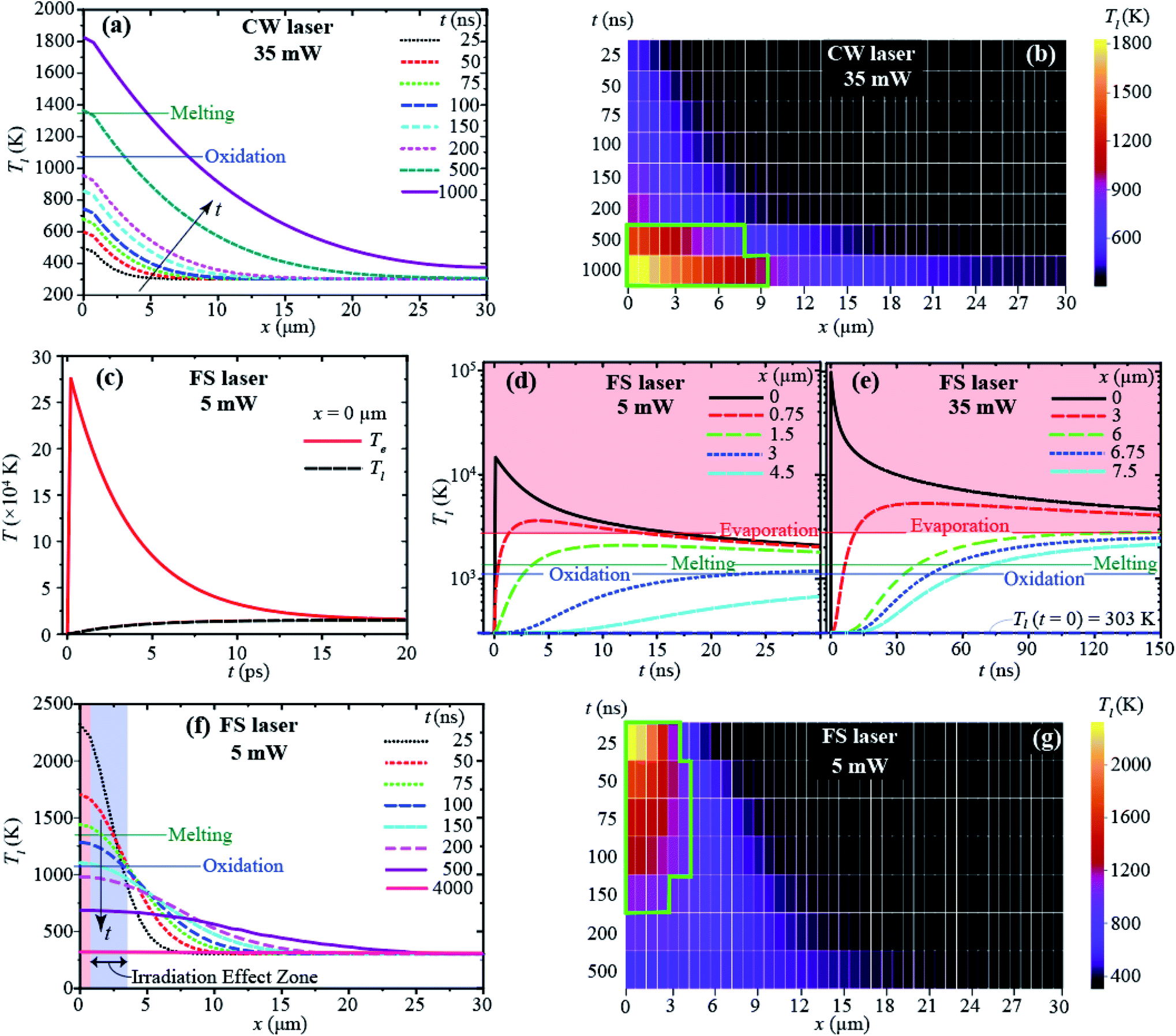 | ||
| Fig. 3 (a) Temperature distribution and (b) heatmap of a modeled CuNW with respect to the distance from the heating area (x, the length direction) at a different heating time (t) when using the CW laser irradiation. (c) Electron and lattice temperatures of the first nodal point (Te and Tl at x = 0) in a short time period after the FS laser pulse (with an average power of 5 mW) starts (<20 ps). Time evolution of lattice temperature (Tl) from the beginning of a laser pulse (300 fs) at five different locations (i.e., x = 0, 0.75, 1.5, 3.0, and 4.5 μm) of the CuNW with an average FS laser power of (d) 5 mW and (e) 35 mW. (f) Temperature distribution and (g) heatmap of the CuNW in the x-direction at different t when using the FS laser with 5 mW average power. The regions surrounded by green lines in (b) and (f) are above the oxidation temperature and vulnerable to oxidation. | ||
With the FS pulse laser irradiation at x = 0, the electron temperature (Te) reaches a very high peak value (∼27.5 × 10⁴ K) within the pulse duration (∼300 fs) as shown in Fig. 3(c), and then it decays rapidly, releasing its energy to phonons (or the lattice). The electron–lattice interaction causes the rise of local Tl,67 and Te reaches almost equilibrium with Tl shortly (<20 ps) after the pulse at x = 0 (Fig. 3(c)). The lattice temperature (Tl) increases and decreases, and for most of the wire (>27 μm), it stays below the Cu melting point (Fig. 3(d)). A non-thermal ablation is expected at the beginning of the irradiated zone (<1 μm, close to the focus spot size) as the lattice temperature is above the evaporation temperature of Cu (Tev = 2840.15 K (ref. 68)), as shown in Fig. 3(d). It is important to point out that such heat is very localized and maintained for a very short time period; Tl can be above the melting point for less than 100 ns only near the heating region (x < 3 μm). FS laser irradiation with an average power of 35 mW as in the CW laser is expected to induce ablation of a much larger area, as shown in Fig. 3(e), up to 6 μm of the CuNW with a higher temperature than Tev. With an average power of 5 mW, Tl drops below the oxidation temperature within 150 ns after a laser pulse, and the entire CuNW will be cooled close to room temperature before the next laser pulse comes (t = 8.33 μs with 120 kHz), as shown in Fig. 3(f) and (g). As Tl is maintained below the oxidation temperature in most regions (x > 4 μm), we expect no significant oxidation. Even if thermal melting and oxidation exist, they are limited to a very local region (near the irradiated region) less than 3 μm. This simulation result is identical to the experimental results that are shown in Fig. 1(b), (c) and S4(a)–(c),† which indicate that FS laser irradiation effect zones are about 2.5–4 μm with different laser powers.
For the sensing application of the welded CuNW with higher electrical conductivity and higher capture efficiency,59,69,70 a single CuNW glucose sensor is fabricated and demonstrated. The sensor fabrication process includes silver electrode printing, gap cutting with a laser, CuNW manipulation, and laser welding. Process details are discussed in the Experimental section. In order to make a functional sensor, the joining of CuNWs to silver electrodes is needed to decrease the contact resistance. The FS laser was selected for the nano-welding of CuNWs to protect the CuNWs from oxidization and deformation due to the laser-induced thermal effect under air conditions. A laser power of 30 mW was used to join a CuNW to the sliver film. Fig. 4(a) shows the SEM image of a CuNW bridging the gap before laser joining. Then the CuNWs were illuminated on both sides by tightly focused laser beams at the position marked with the blue and white circles in Fig. 4(b). Fig. 4(c) shows a cross-sectional SEM image of a laser joined area. A Ge protection layer was deposited during the FIB process for protecting the sample.
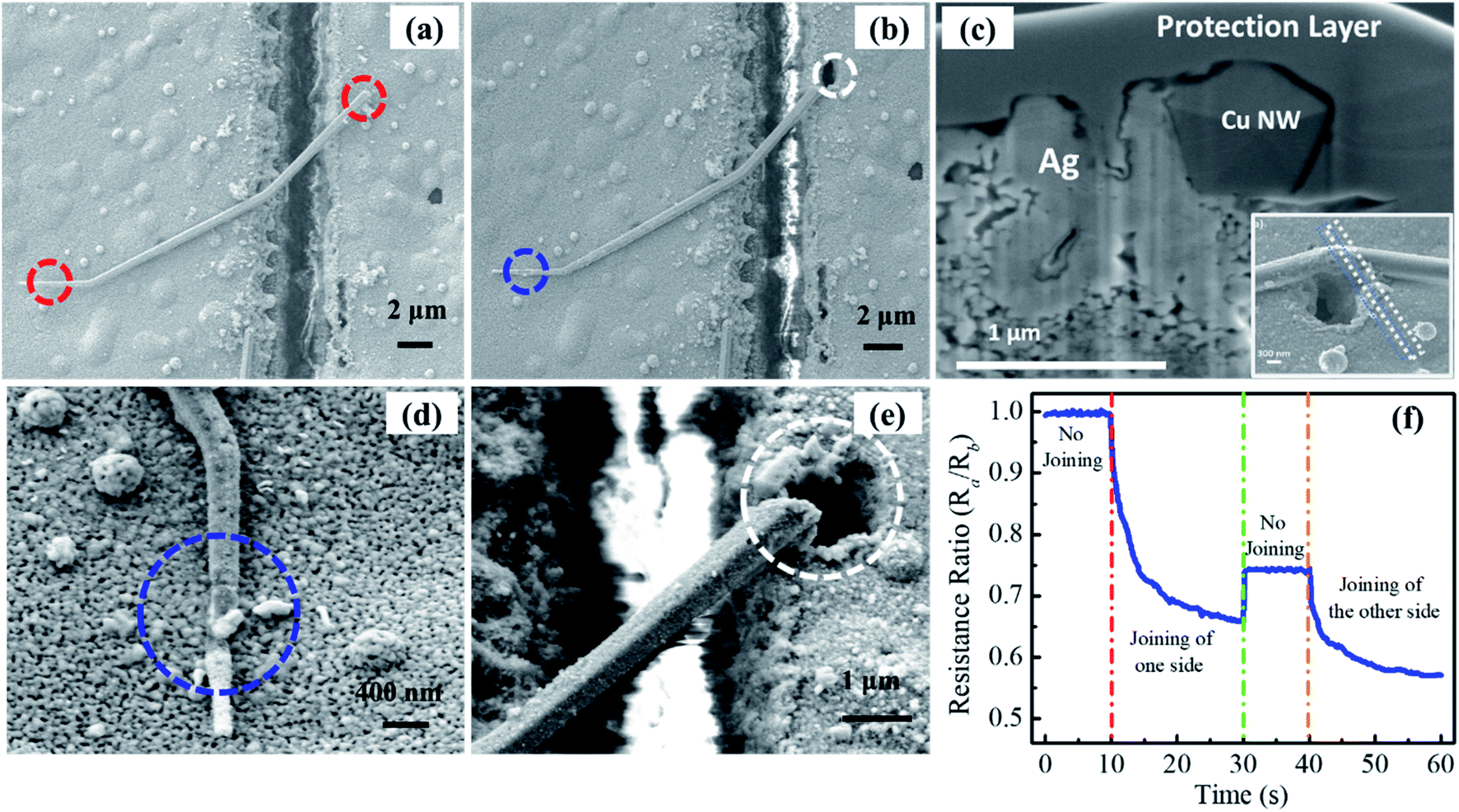 | ||
| Fig. 4 SEM images of a CuNW (a) before laser welding and (b) after FS laser welding, (c) cross-sectional SEM image of the laser-welded area, (d) enlarged image of the blue welding area, (e) enlarged image of the white welding area and (f) real-time resistance change monitoring results during laser welding. | ||
To observe the whole CuNW, the laser focus point is slightly away from the CuNW. It is obvious that the Ag film was melted in the laser irradiation zone. The melted Ag film was partially wrapped around the CuNW and enlarged the contact area, which directly leads to reduce contact resistance. Fig. 4(d) and (e) show the enlarged images of the left and right parts of Fig. 4(b), respectively. In Fig. 4(d), the CuNW is partially damaged, and a part of the CuNW is well embedded into the silver film (as shown by the blue circle). From Fig. 4(e), it is obvious that the NW is partially cut, and a hole is generated in the sliver film (see the white circle position). This difference is due to the surface roughness of the printed silver electrode. The surface of printed silver electrodes is very rough, which will affect the laser focus position and significantly increased the difficulty of constant laser welding. In order to overcome this problem, an in situ resistance measurement is introduced during the nanowire welding process (Fig. 4(f)). The welding process is monitored by the change of the resistance, which provides precise welding monitoring.
The joining situation is further characterized by in situ measurement of the resistance variation via a four-terminal method between after laser joining (Ra) and before laser joining (Rb). The measured resistance ratio as a function of illumination time at a laser power of 30 mW is shown in Fig. 4(f). It is illustrated that the resistance almost keeps unchanged after the single CuNW links the gap. The resistance ratio of Ra to Rb gradually decreases and then becomes flattened during the joining of one side of this CuNW. The resistance ratio increases slightly due to the heterostructure of Cu/Ag before joining the other side, and then it also gradually decreases and then becomes stable in the process of joining the other side. In this experiment, the input electrical current is set as 0.1 μA.
The welded CuNWs were tested for glucose sensing at different concentrations. The sensor shows stable responses with variable glucose concentrations. The detection limit for this sensor is about 10−6 M (1 μM). From Fig. 5(a) and (b), the resistance gradually decreases with increasing glucose concentration from 10−6 M to 1 M [see red circles with error bars and blue squares with error bars]. Moreover, the amperometric detection is carried out by dripping glucose solution with different concentrations onto the welded single CuNW at a voltage of 0.2 V. It is found that the CuNW generates steady-state current for a time interval of 120 s as shown in Fig. 5(c). The response current gradually increases with an increment of glucose concentration from 10−6 M (1 μM) to 1 M. This evidences the single CuNW as a sensor for glucose measurement. Currently, Cu nanowires have been extensively reported as a non-enzyme detection material for glucose,59,70 and the exact mechanism of glucose sensing may be related to the partial oxidization surface of CuNWs.71–73 This surface partial oxidation may be very weak or localized, which cannot be detected by conventional XRD with a detection limit of 3%. The oxidation of glucose in this partially oxidized surface may lead to multi-step reduction from Cu3+, Cu2+, Cu+, to Cu,74,75 and thereby increase the conductivity of CuNWs. As a result, a high glucose concentration intensifies the oxidation reaction and yields a higher current response.
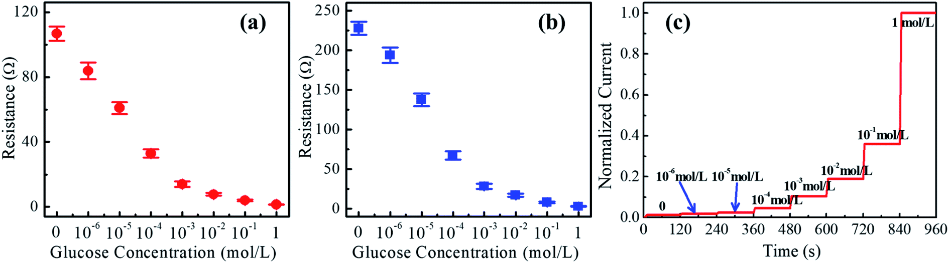 | ||
| Fig. 5 (a) Variation of resistance with the concentration of glucose sample 1 and (b) sample 2. (c) Variation of the normalized response current with time at a voltage of 0.2 V with increasing glucose concentration. | ||
3. Conclusions
Laser welding of CuNWs opens up new possibilities for functional nanodevice development and integration. The simulation and experimental studies conducted demonstrate effective control of material melting and contact welding under laser irradiation. The timescale of laser processing showed a clear impact on the melting and welding of CuNWs and the resultant structural and electrical characteristics. Ultrafast FS laser exposure induced a highly localized non-thermal melting of CuNWs, while CW laser exposure led to significant thermal energy diffusion across the entire nanowire. Computational simulations were conducted to gain an understanding of laser-NW interactions to control material melting and develop high performance welded nanoscale electrical contacts. Simulation studies established heat accumulation overtime under CW laser irradiation leading to melting and oxidation of CuNWs under ambient conditions. However, the highly localized non-thermal heating by the ultrafast FS laser minimized thermal diffusion outside the irradiation zone resulting in a superior surface morphology, prevented metal oxidation, and resulted in reducing contact resistance (contact resistance reduced by over 45%), as verified experimentally. Welding CuNWs with a higher electrical conductivity are promising for nanodevice development and integration. To demonstrate a practical application, we successfully manipulated CuNWs to well-bridge 5 micro-silver film gaps under an AC field and join a single CuNW to the silver film with a focused fs pulsed laser. In situ observation and resistance variation were used to analyze the join situation. It is evident that the contact resistance significantly decreases after joining. Such a welded Cu single nanowire was used for glucose sensing. The experiments showed that the measurement resolution can reach 10−6 M. The present laser processing approach provides an effective strategy for fabricating 1D–3D electronic devices through nanoscale welding of diverse metallic and semiconducting NWs.4. Experimental section
Cu nanowires
CuNWs were prepared with a modified hydrothermal method, according to ref. 76. 1348 mg octadecylamine (ODA) was added to 100 ml of copper chloride (426 mg) solution and vigorously stirred for 5 hours to form a blue emulsion. Then, the solution was transferred into a Teflon-lined autoclave of 125 ml capacity and heated at 150 °C for 72 hours. After cooling down the autoclave to room temperature, the supernatant was poured away, and the CuNW solution was kept at the bottom. Finally, CuNWs were washed with ethanol 2–4 times to remove ODA.Silver electrodes
Silver (Ag) electrodes were printed by using an Optomec aerosol jet printing system (AJ 200) with Ag nanoparticle ink (CLARIANT). The diameter of the Ag nanoparticle is about 30–40 nm. In this experiment, silver electrodes were printed with 80 μm line width and 35% overlap. The printed silver electrodes were cured in a furnace for 1 hour at a temperature of 125 °C. Regular photo paper was selected as a substrate due to its relatively high printability and high flexibility. The processing speed was set as 2 mm s−1. The thickness of the printed Ag electrodes was around 3–4 μm.Cutting of silver films with a femtosecond pulsed laser
Fig. S4(a)† shows a schematic diagram of the 3D laser direct writing system. The fiber laser system (Model: Cazadero, Calmar Laser Inc.) generates femtosecond (fs) pulse chains, of which the main parameters are listed as follows: pulse width ∼350 fs, 1030 nm central wavelength, 120 kHz repetition rate and 2.5 W average power. The fs pulsed laser passed through a shutter, optical isolator, adjustable attenuator, dichroic mirror and microscope objective lens. Then it was used to cut silver films on a 3D translation stage. The laser beam passed into a vertical microscope system and was focused by a long working distance and high numerical aperture ×100 objective lens (0.8 NA). Real-time observation of the laser writing process was performed with a charge-coupled device (CCD). The laser writing process was implemented with a scanning program-controlled design. Fig. S3(b)† shows an SEM image of cutting of silver films at an incident laser fluence of 2.75 J cm−2, the corresponding average power is 400 mW, and the gap width is around 3.6 μm. The right picture [Fig. S4(c)†] shows a Liu-plot of ablation areas (D-square) as a function of incident laser fluence.77 It demonstrated that the D-square gradually increased with an increment of incident laser fluence. The ablation threshold of the silver films is 2.53 J cm−2. During the cutting of the silver films, the laser power was adjusted to 400 mW and the speed of the 3D translation stage was 20 mm min−1. Thus, the silver film was cut to form the trench-structured electrodes with a gap of 2–4 μm.Manipulation of CuNWs with a dielectrophoresis method
After the preparation of CuNWs and cutting of silver films, CuNW solution was added dropwise onto the gap and CuNWs were manipulated by a DEP method. In this experiment, the manipulation of CuNWs was performed by adding alternating current (AC, Model: GWinstek SFG-1013) with different parameters on both sides of the gap; the schematic diagram is presented in Fig. S4(a) and (b).† Fig. S4(e) and (f)† show CuNW solution droplet transfer and CuNW alignment by a DEP force, respectively. The time-averaged DEP force acting on the CuNWs is estimated based on eqn (1).29 | (1) |
Nanowire selection and cutting
During the manipulation of CuNWs with AC bias, it is found that several CuNWs well link the gap. Here, the main target of this study is to fabricate a single NW device. So only one CuNW bridging the gap is needed, other CuNWs bridging the gap should be cut off with an FS pulsed laser. For cutting CuNWs, 70 mW laser power was induced at the middle position of these CuNWs. Fig. S4(e)† shows a CuNW before laser cutting and Fig. S5(f)† shows the CuNW after cutting with the FS laser.Single-temperature 1-D heat diffusion model
The temperature distribution in the CuNW and its evolution during the CW laser heating are calculated by using a single-temperature 1-D heat diffusion model and the finite difference method. The energy balance in control volume of each nodal point (m) is used as the governing equation:78–80| Qlaser + Qcond − Qconv − Qrad = ΔEst, | (2) |
Two-temperature model
With a short pulse of high-intensity laser irradiation, nonequilibrium between electron and lattice systems dynamically changes, and to address this nonequilibrium dynamics, the electron and lattice temperatures of the CuNW (Te and Tl) are separately calculated. As in the analysis of the CW laser, a 1-D model and FDM are employed, but for each nodal point, the thermal energy balances for the electron and lattice are considered, given by:84For electron Te,
| Qlaser − Qel→latt + Qel,cond = ΔEel, | (3) |
For lattice Tl,
| Qel→latt + Qlatt,cond − Qconv − Qrad = ΔElatt. | (4) |
Author contributions
Yongchao Yu and Yangbao Deng contributed equally to this work. Computational simulations are carried out by Md Abdullah Al Hasan.Conflicts of interest
We have no conflicts of interest to declare.Acknowledgements
This work is partially supported by a seed grant of the University of Tennessee, Knoxville. And this work was also performed in part at the Oak Ridge National Laboratory, operated by UT-Battelle for the U.S. Department of Energy under contract no. DE-AC05-00OR22725.References
- A. L. Falk, F. H. Koppens, L. Y. Chun, K. Kang, N. de Leon Snapp, A. V. Akimov, M.-H. Jo, M. D. Lukin and H. Park, Nat. Phys., 2009, 5, 475 Search PubMed.
- J.-Y. Lee, S. T. Connor, Y. Cui and P. Peumans, Nano Lett., 2008, 8, 689 CrossRef CAS PubMed.
- L. Hu, H. S. Kim, J.-Y. Lee, P. Peumans and Y. Cui, ACS Nano, 2010, 4, 2955 CrossRef CAS PubMed.
- J. Lee, P. Lee, H. Lee, D. Lee, S. S. Lee and S. H. Ko, Nanoscale, 2012, 4, 6408 RSC.
- Y. NormanáZhou, J. Mater. Chem., 2012, 22, 12997 RSC.
- R. Mehta, S. Chugh and Z. Chen, Nano Lett., 2015, 15, 2024 CrossRef CAS PubMed.
- R.-Z. Li, A. Hu, T. Zhang and K. D. Oakes, ACS Appl. Mater. Interfaces, 2014, 6, 21721 CrossRef CAS PubMed.
- C. Yan, W. Kang, J. Wang, M. Cui, X. Wang, C. Y. Foo, K. J. Chee and P. S. Lee, ACS Nano, 2013, 8, 316 CrossRef PubMed.
- S. Choi, J. Park, W. Hyun, J. Kim, J. Kim, Y. B. Lee, C. Song, H. J. Hwang, J. H. Kim and T. Hyeon, ACS Nano, 2015, 9, 6626 CrossRef CAS PubMed.
- S. Hong, H. Lee, J. Lee, J. Kwon, S. Han, Y. D. Suh, H. Cho, J. Shin, J. Yeo and S. H. Ko, Adv. Mater., 2015, 27, 4744 CrossRef CAS PubMed.
- K. Takei, T. Takahashi, J. C. Ho, H. Ko, A. G. Gillies, P. W. Leu, R. S. Fearing and A. Javey, Nat. Mater., 2010, 9, 821 CrossRef CAS PubMed.
- P. Peng, H. Huang, A. Hu, A. P. Gerlich and Y. N. Zhou, J. Mater. Chem., 2012, 22, 15495 RSC.
- Y. Yu, P. C. Joshi, J. Wu and A. Hu, ACS Appl. Mater. Interfaces, 2018, 10, 34005 CrossRef CAS PubMed.
- O. Englander, D. Christensen, J. Kim, L. Lin and S. J. Morris, Nano Lett., 2005, 5, 705 CrossRef CAS PubMed.
- L. Dong, J. Bush, V. Chirayos, R. Solanki, J. Jiao, Y. Ono, J. F. Conley and B. D. Ulrich, Nano Lett., 2005, 5, 2112 CrossRef CAS PubMed.
- C. S. Lao, J. Liu, P. Gao, L. Zhang, D. Davidovic, R. Tummala and Z. L. Wang, Nano Lett., 2006, 6, 263 CrossRef CAS PubMed.
- Z. Yang, M. Wang, Q. Zhao, H. Qiu, J. Li, X. Li and J. Shao, ACS Appl. Mater. Interfaces, 2017, 9, 22837 CrossRef CAS PubMed.
- Y. Huang, X. Duan, Q. Wei and C. M. Lieber, Science, 2001, 291, 630 CrossRef CAS PubMed.
- G. Yu, A. Cao and C. M. Lieber, Nat. Nanotechnol., 2007, 2, 372 CrossRef CAS PubMed.
- Z. Fan, J. C. Ho, Z. A. Jacobson, R. Yerushalmi, R. L. Alley, H. Razavi and A. Javey, Nano Lett., 2008, 8, 20 CrossRef CAS PubMed.
- D. R. Kim, C. H. Lee and X. Zheng, Nano Lett., 2010, 10, 1050 CrossRef CAS PubMed.
- D. Whang, S. Jin, Y. Wu and C. M. Lieber, Nano Lett., 2003, 3, 1255 CrossRef CAS.
- E. R. Dufresne and D. G. Grier, Rev. Sci. Instrum., 1998, 69, 1974 CrossRef CAS.
- R. Agarwal, K. Ladavac, Y. Roichman, G. Yu, C. M. Lieber and D. G. Grier, Opt. Express, 2005, 13, 8906 CrossRef PubMed.
- J. K. Valley, S. Neale, H.-Y. Hsu, A. T. Ohta, A. Jamshidi and M. C. Wu, Lab Chip, 2009, 9, 1714 RSC.
- W. Hu, K. S. Ishii and A. T. Ohta, Appl. Phys. Lett., 2011, 99, 094103 CrossRef.
- S. Tottori, L. Zhang, F. Qiu, K. K. Krawczyk, A. Franco-Obregón and B. J. Nelson, Adv. Mater., 2012, 24, 811 CrossRef CAS PubMed.
- C. H. Lee, D. R. Kim and X. Zheng, Nano Lett., 2010, 10, 5116 CrossRef CAS PubMed.
- H. A. Pohl, The Behavior of Neutral Matter in Nonuniform Electric Fields 1978 Search PubMed.
- W. Lu and C. M. Lieber, in Nanoscience and Technology: A Collection of Reviews from Nature Journals, World Scientific, 2010, p. 137 Search PubMed.
- H. Yan, H. S. Choe, S. Nam, Y. Hu, S. Das, J. F. Klemic, J. C. Ellenbogen and C. M. Lieber, Nature, 2011, 470, 240 CrossRef CAS PubMed.
- J. Kim, H.-C. Lee, K.-H. Kim, M.-S. Hwang, J.-S. Park, J. M. Lee, J.-P. So, J.-H. Choi, S.-H. Kwon and C. J. Barrelet, Nat. Nanotechnol., 2017, 12, 963 CrossRef CAS PubMed.
- Y. Fang, Z. Li, Y. Huang, S. Zhang, P. Nordlander, N. J. Halas and H. Xu, Nano Lett., 2010, 10, 1950 CrossRef CAS PubMed.
- C. Rewitz, G. Razinskas, P. Geisler, E. Krauss, S. Goetz, M. Pawłowska, B. Hecht and T. Brixner, Phys. Rev. Appl., 2014, 1, 014007 CrossRef.
- A. Hu, P. Peng, H. Alarifi, X. Zhang, J. Guo, Y. Zhou and W. Duley, J. Laser Appl., 2012, 24, 042001 CrossRef.
- Y. Lu, J. Y. Huang, C. Wang, S. Sun and J. Lou, Nat. Nanotechnol., 2010, 5, 218 CrossRef CAS PubMed.
- P. Peng, L. Liu, A. P. Gerlich, A. Hu and Y. N. Zhou, Part. Part. Syst. Charact., 2013, 30, 420 CrossRef CAS.
- A. Hu, J. Guo, H. Alarifi, G. Patane, Y. Zhou, G. Compagnini and C. Xu, Appl. Phys. Lett., 2010, 97, 153117 CrossRef.
- H. Tohmyoh and S. Fukui, Phys. Rev. B: Condens. Matter Mater. Phys., 2009, 80, 155403 CrossRef.
- T.-B. Song, Y. Chen, C.-H. Chung, Y. Yang, B. Bob, H.-S. Duan, G. Li, K.-N. Tu, Y. Huang and Y. Yang, ACS Nano, 2014, 8, 2804 CrossRef CAS PubMed.
- A. T. Bellew, H. G. Manning, C. Gomes da Rocha, M. S. Ferreira and J. J. Boland, ACS Nano, 2015, 9, 11422 CrossRef CAS PubMed.
- A. Vafaei, A. Hu and I. A. Goldthorpe, Nano-Micro Lett., 2014, 6, 293 CrossRef.
- J. S. Oh, J. S. Oh, J. H. Shin, G. Y. Yeom and K. N. Kim, J. Nanosci. Nanotechnol., 2015, 15, 8647 CrossRef CAS PubMed.
- T. Tokuno, M. Nogi, M. Karakawa, J. Jiu, T. T. Nge, Y. Aso and K. Suganuma, Nano Res., 2011, 4, 1215 CrossRef CAS.
- E. C. Garnett, W. Cai, J. J. Cha, F. Mahmood, S. T. Connor, M. G. Christoforo, Y. Cui, M. D. McGehee and M. L. Brongersma, Nat. Mater., 2012, 11, 241 CrossRef CAS PubMed.
- S. Han, S. Hong, J. Ham, J. Yeo, J. Lee, B. Kang, P. Lee, J. Kwon, S. S. Lee and M. Y. Yang, Adv. Mater., 2014, 26, 5808 CrossRef CAS PubMed.
- S. Dai, Q. Li, G. Liu, H. Yang, Y. Yang, D. Zhao, W. Wang and M. Qiu, Appl. Phys. Lett., 2016, 108, 121103 CrossRef.
- L. Lin, L. Liu, K. Musselman, G. Zou, W. W. Duley and Y. N. Zhou, Adv. Funct. Mater., 2016, 26, 5979 CrossRef CAS.
- L. Lin, G. Zou, L. Liu, W. W. Duley and Y. N. Zhou, Appl. Phys. Lett., 2016, 108, 203107 CrossRef.
- S. J. Henley, M. Cann, I. Jurewicz, A. Dalton and D. Milne, Nanoscale, 2014, 6, 946 RSC.
- J. A. Spechler and C. B. Arnold, Appl. Phys. A: Mater. Sci. Process., 2012, 108, 25 CrossRef CAS.
- Q. Li, G. Liu, H. Yang, W. Wang, S. Luo, S. Dai and M. Qiu, Appl. Phys. Lett., 2016, 108, 193101 CrossRef.
- G. Satoh, C. Qiu, S. Naveed and Y. L. Yao, J. Manuf. Sci. Eng., 2015, 137, 011012 CrossRef.
- L. Lin, L. Liu, P. Peng, G. Zou, W. W. Duley and Y. N. Zhou, Nanotechnology, 2016, 27, 125201 CrossRef PubMed.
- H. Yang, J. Lu, P. Ghosh, Z. Chen, W. Wang, H. Ye, Q. Yu, M. Qiu and Q. Li, Appl. Phys. Lett., 2018, 112, 071108 CrossRef.
- I. Shchatsinin, T. Laarmann, N. Zhavoronkov, C. P. Schulz and I. V. Hertel, J. Chem. Phys., 2008, 129, 204308 CrossRef PubMed.
- R. R. Gattass and E. Mazur, Nat. Photonics, 2008, 2, 219 CrossRef CAS.
- S.-S. Wellershoff, J. Hohlfeld, J. Güdde and E. Matthias, Appl. Phys. A: Mater. Sci. Process., 1999, 69, S99 CAS.
- Y. Zhang, L. Su, D. Manuzzi, H. V. E. de los Monteros, W. Jia, D. Huo, C. Hou and Y. Lei, Biosens. Bioelectron., 2012, 31, 426 CrossRef CAS PubMed.
- R. R. Gattass and E. Mazur, Nat. Photonics, 2008, 2, 219 CrossRef CAS.
- K. Sugioka and Y. Cheng, Light: Sci. Appl., 2014, 3, e149 CrossRef CAS.
- C. S. Nathala, A. Ajami, W. Husinsky, B. Farooq, S. I. Kudryashov, A. Daskalova, I. Bliznakova and A. Assion, Appl. Phys. A: Mater. Sci. Process., 2016, 122, 107 CrossRef.
- X. Chen, Y. Chen, J. Dai, M. Yan, D. Zhao, Q. Li and M. Qiu, Nanoscale, 2014, 6, 1756 RSC.
- S. Holman, R. Lawrence and L. Barr, Proc. Am. Acad. Arts Sci., 1895, 31, 218–233 CrossRef.
- U. Nerle and M. K. Rabinal, IOSR J. Appl. Phys., 2013, 5, 1 CrossRef.
- M. Kaur, K. Muthe, S. Despande, S. Choudhury, J. Singh, N. Verma, S. Gupta and J. Yakhmi, J. Cryst. Growth, 2006, 289, 670 CrossRef CAS.
- J. K. Chen, D. Y. Tzou and J. E. Beraun, Int. J. Heat Mass Transfer, 2005, 48, 501 CrossRef CAS.
- Y. Bentor, Periodic Table: Copper, http://www.chemicalelements.com/elements/cu.html, accessed, August 30, 2019 Search PubMed.
- Y. Jianfeng, Z. Guisheng, H. Anming and Y. N. Zhou, J. Mater. Chem., 2011, 21, 15981 RSC.
- J. Huang, Z. Dong, Y. Li, J. Li, J. Wang, H. Yang, S. Li, S. Guo, J. Jin and R. Li, Sens. Actuators, B, 2013, 182, 618 CrossRef CAS.
- X. Kang, Z. Mai, X. Zou, P. Cai and J. Mo, Anal. Biochem., 2007, 363, 143 CrossRef CAS PubMed.
- T. S. Babu, T. Ramachandran and B. Nair, Microchim. Acta, 2010, 169, 49 CrossRef CAS.
- L. Zhang, J. Zhang, C. Yang, G. Zhao, J. Mu and Y. Wang, RSC Adv., 2015, 5, 82998 RSC.
- J. Luo, S. Jiang, H. Zhang, J. Jiang and X. Liu, Anal. Chim. Acta, 2012, 709, 47 CrossRef CAS PubMed.
- T.-K. Huang, K.-W. Lin, S.-P. Tung, T.-M. Cheng, I.-C. Chang, Y.-Z. Hsieh, C.-Y. Lee and H.-T. Chiu, J. Electroanal. Chem., 2009, 636, 123 CrossRef CAS.
- Y. Shi, H. Li, L. Chen and X. Huang, Sci. Technol. Adv. Mater., 2005, 6, 761 CrossRef CAS.
- J. Liu, Opt. Lett., 1982, 7, 196 CrossRef CAS PubMed.
- T. L. Bergman, F. P. Incropera, D. P. DeWitt and A. S. Lavine, Fundamentals of Heat and Mass Transfer, John Wiley & Sons, 2011 Search PubMed.
- J. H. Lienhard, A Heat Transfer Textbook, Courier Corporation, 2011 Search PubMed.
- Y. A. Cengel, Heat Transfer: A Practical Approach, McGraw-Hill, New York, 2nd edn, 2002 Search PubMed.
- D. Bergström, Luleå Tekniska Universitet, Doctoral thesis, 2008.
- F. P. Incropera, A. S. Lavine, T. L. Bergman and D. P. DeWitt, Fundamentals of Heat and Mass Transfer, Wiley, 2007 Search PubMed.
- Z. Yang, J. Hao, S. Yuan, S. Lin, H. M. Yau, J. Dai and S. P. Lau, Adv. Mater., 2015, 27, 3748 CrossRef CAS PubMed.
- S. S. Wellershoff, J. Hohlfeld, J. Güdde and E. Matthias, Appl. Phys. A: Mater. Sci. Process., 1999, 69, S99 CAS.
- L. L. Taylor, R. E. Scott and J. Qiao, Opt. Mater. Express, 2018, 8, 648 CrossRef CAS.
- Z. Lin, L. V. Zhigilei and V. Celli, Phys. Rev. B: Condens. Matter Mater. Phys., 2008, 77, 075133 CrossRef.
- Y. Wang, Z. Lu and X. Ruan, J. Appl. Phys., 2016, 119, 225109 CrossRef.
Footnote |
| † Electronic supplementary information (ESI) available: Details of the CuNW self-joining phenomenon, a comparison study between different laser irradiation on CuNWs, sensing unit fabrication process, and details of computational modeling. See DOI: 10.1039/c9na00740g |
| This journal is © The Royal Society of Chemistry 2020 |