
 Open Access Article
 This Open Access Article is licensed under a Creative Commons Attribution-Non Commercial 3.0 Unported Licence
Does carrier velocity saturation help to enhance fmax in graphene field-effect transistors?†
Pedro C.
Feijoo
 *a,
Francisco
Pasadas
a,
Marlene
Bonmann
b,
Muhammad
Asad
b,
Xinxin
Yang
b,
Andrey
Generalov
c,
Andrei
Vorobiev
b,
Luca
Banszerus
d,
Christoph
Stampfer
d,
Martin
Otto
e,
Daniel
Neumaier
e,
Jan
Stake
b and
David
Jiménez
a
*a,
Francisco
Pasadas
a,
Marlene
Bonmann
b,
Muhammad
Asad
b,
Xinxin
Yang
b,
Andrey
Generalov
c,
Andrei
Vorobiev
b,
Luca
Banszerus
d,
Christoph
Stampfer
d,
Martin
Otto
e,
Daniel
Neumaier
e,
Jan
Stake
b and
David
Jiménez
a
aUniversitat Autònoma de Barcelona, 08193 Cerdanyola del Vallès, Spain. E-mail: PedroCarlos.Feijoo@uab.cat
bChalmers University of Technology, SE-41296 Gothenburg, Sweden
cAalto University, FI-00076 Helsinki, Finland
d2nd Institute of Physics, RWTH Aachen University, 52074 Aachen, Germany
eAdvanced Microelectronic Center Aachen, AMO GmbH, 52074 Aachen, Germany
First published on 24th July 2020
Abstract
It has been argued that current saturation in graphene field-effect transistors (GFETs) is needed to get optimal maximum oscillation frequency (fmax). This paper investigates whether velocity saturation can help to get better current saturation and if that correlates with enhanced fmax. We have fabricated 500 nm GFETs with high extrinsic fmax (37 GHz), and later simulated with a drift–diffusion model augmented with the relevant factors that influence carrier velocity, namely: short-channel electrostatics, saturation velocity effect, graphene/dielectric interface traps, and self-heating effects. Crucially, the model provides microscopic details of channel parameters such as carrier concentration, drift and saturation velocities, allowing us to correlate the observed macroscopic behavior with the local magnitudes. When biasing the GFET so all carriers in the channel are of the same sign resulting in highly concentrated unipolar channel, we find that the larger the drain bias is, both closer the carrier velocity to its saturation value and the higher the fmax are. However, the highest fmax can be achieved at biases where there exists a depletion of carriers near source or drain. In such a situation, the highest fmax is not found in the velocity saturation regime, but where carrier velocity is far below its saturated value and the contribution of the diffusion mechanism to the current is comparable to the drift mechanism. The position and magnitude of the highest fmax depend on the carrier concentration and total velocity, which are interdependent and are also affected by the self-heating. Importantly, this effect was found to severely limit radio-frequency performance, reducing the highest fmax from ∼60 to ∼40 GHz.
Introduction
The development of new-generation radio-frequency (RF) electronics enables extending the range of advanced applications within the areas of communication, security imaging, quality control, medicine etc.1 For the sustainable development, new materials with enhanced electronic properties are required. Graphene is considered as a promising channel material for RF field-effect transistors due to its intrinsically high charge carrier mobility (up to 2 × 105 cm2 V−1 s−1) and saturation velocity (4 × 107 cm s−1).2–6 However, RF performance of the graphene field-effect transistors (GFETs) was limited until recently by several factors, for example, a relatively high drain conductance due to zero bandgap, a high graphene/metal contact resistance and the extrinsic carrier scattering by charged defects.7–11 Continuous efforts in the study of GFETs have resulted in an important improvement of the RF figures of merit (FoMs): the extrinsic cutoff (transit) frequency (fT,x) and maximum frequency of oscillation (fmax).12–17 This enhancement has been enabled, in particular, by the use of GFET models, which have allowed for clarifying and overcoming RF performance limitations.18–27 Recently, values of fT,x = 34 GHz and fmax = 37 GHz for GFETs with chemical vapor deposited graphene and a gate length (Lg) of 500 nm were reported by some of us.28 These RF FoMs outperform the ones obtained in other graphene-based transistors with similar Lg, although higher values were achieved for shorter Lg.29 Furthermore, these values of fT,x and fmax surpassed those of the best Si MOSFETs with similar gate lengths.30 The achievement has been obtained by a combination of different improvements of the GFET design and fabrication process that have resulted in high saturation velocity, low contact resistance, and reduced extrinsic pad capacitances.A question that remains to be answered is whether operating the GFET in a saturation velocity regime actually helps to get the highest fmax. The resolution to this problem needs a simulation tool that considers the factors that affect the current saturation, namely, short-channel effects, velocity saturation effects, and self-heating effects (SHE). Our preliminary analysis indicated that these effects can be significant when a GFET works at relatively high drain fields, above 1 V μm−1. In previous works, a self-consistent simulator that accounted for short-channel and velocity saturation effects was developed to investigate the RF performance and scalability of GFETs.24,25 That simulator has been updated in the present work including the SHE with two purposes: to study the DC and RF performance of the prototype 500 nm GFET presented in ref. 28 and to explore whether there is still room for fmax improvement by exploiting the saturation velocity regime.
This paper thoroughly studies the impact of drain current saturation on RF performance as the interplay between carrier concentration (the gradient of which triggers the diffusion current) and velocity, which has only been slightly addressed before.21 To investigate GFET performance, we follow an approach that consists firstly in solving the drift–diffusion equation self-consistently with the two-dimensional Poisson's equation to get the DC characteristics.24 This set of equations is, in turn, coupled with the heat transfer equation that models the SHE. Then RF performance is obtained from a quasi-static small-signal model, whose parameters are extracted from linearization of the DC simulations.25 Such a methodology is thoroughly described in Methods. The combined analysis of DC and RF simulations allows us to assess the influence of graphene electrical properties as the saturation velocity and low-field mobility, and other limiting factors as, for instance, the contact resistance, the interface traps and extrinsic capacitances. Thereby, we have obtained insights on the mechanisms defining the DC and RF performance of GFETs, which are discussed in Results and discussion. Particularly, we have addressed the question whether velocity saturation can help to get better current saturation and if that correlates with enhanced fmax. Finally, the conclusions are drawn in the Conclusions section.
Methods
Device structure and description of the self-consistent simulator
To investigate the bias dependence of RF performance and its relation with current saturation, we have numerically investigated the prototype GFET with high extrinsic fT,x and fmax described in ref. 28. Fig. 1 shows the GFET scanning electron microscope (SEM) image of the device and a schematic view of one of the two fingers. The GFET gate length and total gate width were Lg = 500 nm and Wg = 2 × 15 μm, respectively. The length of each ungated region of the channel was Lung = 100 nm. The graphene layer was encapsulated between insulating layers of Al2O3 and SiO2 with thicknesses of tt = 22 nm and tb = 1 μm, respectively. The relatively thick SiO2 allows for reduction of the parasitic pad capacitances.28 High-resistivity (larger than 10 kΩ cm) silicon was used as substrate with the aim of minimizing the substrate-related microwave loss in the GFET contact pads and transmission lines of the prospective devices.31 Details on the GFET fabrication are included in Section S1 of the ESI.†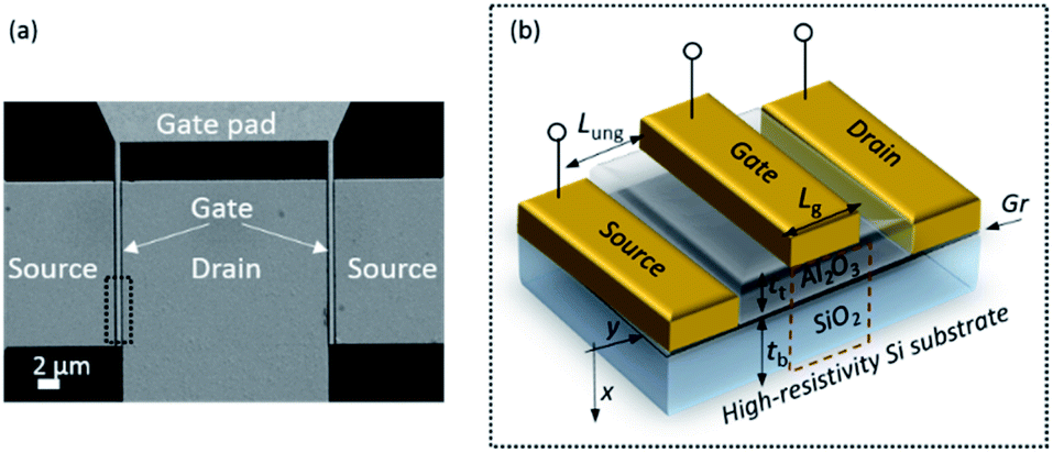 | ||
| Fig. 1 (a) GFET SEM image and (b) schematic view (not drawn to scale) of the gate region indicated in (a). The dashed rectangle encloses the domain where the Poisson's equation is solved. | ||
The GFET was simulated using the method described in ref. 24 and 25, which consists in solving self-consistently 2D Poisson's equation and 1D drift–diffusion transport equation. The dashed rectangle in Fig. 1(b) encloses the active area of the transistor and corresponds to the domain where the Poisson's equation is solved. The simulator obtains the stationary distributions of graphene electrical parameters along the channel as a function of the voltages applied to the gate-source and drain-source terminals (Vgs and Vds, respectively). Specifically, it is possible to get the local parameters such as the charge carrier concentration for both electrons (n) and holes (p), the carrier field-dependent mobility (μ), the separate currents and carrier velocities driven by both drift (νdrift) and diffusion mechanisms (νdiff), the Dirac energy (ED = −qψ) and the quasi-fermi energy (EF = −qV). The details of the simulator and the different carrier velocity definitions used in this work can be found in Sections S2 and S3, respectively, of the ESI.† Key parameters as the flatband voltage (Vgs0), the residual charge carrier concentration (ρ0), the low-field mobility (μLF), and the contact resistance (Rc) were extracted from measured low-Vds transfer curves (Ids–Vgs) with holding time of 1 s at each bias point (see Section S4 of the ESI†). After that, we fitted the measured output characteristics (Ids–Vds), which were obtained upon application of a holding time of 30 s per measured point. That time is long enough for the trapping/de-trapping processes to stabilize at high fields.32 The fitting parameters are the interface trap density (Nit), the energy of optical phonons (ℏΩ), whose emission limits carrier drift velocity, and the effective thermal resistance (Rth). The latter will be discussed below. The model for the saturation velocity νsat is given by:33
 | (1) |
 | (2) |
Eqn (1) and (2) show that saturation velocity strongly depends on carrier concentration. Moreover, an increase in temperature slightly decreases νsat. These dependencies can be seen in Fig. 2, where νsat has been represented for typical values of carrier concentration at several temperatures.
 | ||
| Fig. 2 Carrier saturation velocity as a function of the carrier concentration for different temperatures. The value of the optical phonon energy used has been ℏΩ = 0.10 eV. | ||
We have used the following equation to model the field-dependent mobility μ(y) as a function of the local electric field and saturation velocity, and thereby, also on ρsh(y) and T:
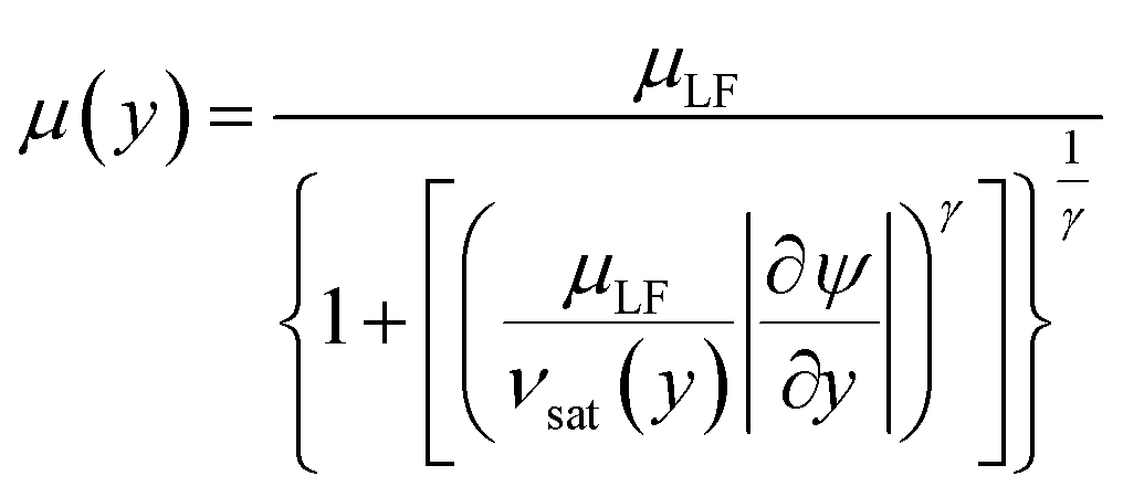 | (3) |
Unlike our previous works, we have included the SHE in the self-consistent loop of the GFET simulator. This means that we assume that the temperature of the GFET rises because the heat dissipated in graphene by the Joule effect finds difficulty to spread out of the device through the surrounding layers. By using the simplest thermal model, the temperature of the graphene channel can be expressed as:
| T − T0 = RthPdis | (4) |
 | (5) |
 is the intrinsic drain-to-source voltage. This model considers an average temperature for the whole graphene sheet, so it neglects any local temperature deviation. It also neglects any temperature deviation at the proximities of the contacts, which could be a problem for graphene devices with Lg below 300 nm.35 Our previous measurements indicate that we can neglect the heat dissipated through the gate stack and at the proximity of the contacts,28 so the applied model is expected to work properly for the analyzed device.
Using the values for mobility and carrier concentration obtained in this study we estimate the mean free path (MFP) by the semiclassical model described in ref. 6 in the 10–100 nm range. Since the MFP is much shorter than the source-to-drain length (Lg + 2Lung), it is confirmed that the drift–diffusion transport mechanism is appropriate for describing the electronic transport in the examined GFET. Transistors with shorter channel lengths should be analyzed with ballistic or quantum models, which is beyond the scope of this work.
Small-signal model of the GFET and derived RF performance
For the analysis of the RF performance, we consider the GFET as a two-port network in common-source configuration. The device is characterized by its extrinsic admittance matrix Y. This matrix is calculated in two steps. First, the intrinsic admittance matrix Y′ is determined by the intrinsic small-signal equivalent circuit model assuming quasi-static operation.36 Then the extrinsic Y matrix is obtained embedding the intrinsic GFET in a simplified extrinsic circuit of lumped elements, which consists of parasitic resistances at each of the three terminals and parasitic capacitances at both the input and the output ports. Since tb ≫ tt, the back-gate capacitance is much smaller than the top-gate capacitance, so we can neglect the influence of the substrate capacitance in Y′. Tunneling currents through any of the dielectrics are also neglected.Transconductance gm and output conductance gsd can be obtained from the derivatives of Ids respect to the intrinsic bias voltages  , respectively. Then, the small-signal capacitances are determined from the charges associated to each of the terminals (Qi, with i = s, d or g). They have been defined assuming a charge conserving Ward–Dutton's linear charge partition scheme.36 The transcapacitances Cgs, Cgd, Csd, Cdg are obtained as the derivative of charge at terminal i with respect to the intrinsic voltage at terminal j,
 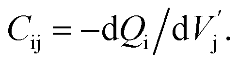 For the calculation of the small-signal parameters, we assume that the temperature is constant at a given bias point. A full description of the small-signal parameter and extrinsic admittance matrix calculation can be found in Section S5 of the ESI.† Finally, the RF FoMs fT,x and fmax are extracted from the current gain and unilateral power gain that result from the Y matrix.37
Results and discussion
First, we reproduced the experimental DC characteristics following the methodology described in Methods. Fig. 3(a) shows the measured output characteristics of the GFET and their comparison with the simulations, where the parameters used are presented in Table 1. The estimated Nit was found to be lower than 1012 eV−1 cm−2, a value below which the influence of interface traps is negligible, as shown in Section S8 of the ESI.† The best fitting value of the Rc is 11 Ω, which includes the metal/graphene contact resistance at both drain and source together with the access resistances of the ungated graphene regions. Thus, the width specific contact resistivity results in RcWg/2 = 165 Ω μm. The width specific metal/graphene contact resistivity of approximately 90 Ω μm, evaluated applying the drain resistance model to the transfer characteristic, agrees with the value of 95 Ω μm obtained by transfer length measurements (which exclude access resistance). From the fitting done in Fig. 3(a), we obtained a value of 2.7 × 10⁴ K W−1 for the Rth, which agrees with the order of magnitude of calculations based on the model by Pop et al.,22,33 of around 3–4 × 10⁴ K W−1. Our simulator also allowed us to calculate GFET temperature as a function of the bias, shown in Fig. 3(b), and ranging between 300 and 1000 K. The simulated temperatures are similar to the ones obtained in previous works analyzing gate leakage current as a thermo–sensitive parameter.38 | ||
| Fig. 3 (a) Measured (squares) and modelled (solid lines) DC output characteristics of a GFET. Dashed lines correspond to the simulated current neglecting SHE. (b) GFET temperature as a function of the drain bias due to self-heating. | ||
| Parameter | Optimized value |
|---|---|
| V gs0 | 2.2 V |
| ρ 0 | 2.9 × 1011 cm−2 |
| μ LF | 2.0 × 103 cm2 V−1 s−1 |
| R c | 11 Ω |
| N it | <1012 eV−1 cm−2 |
| ℏΩ | 0.10 eV |
| R th | 2.7 × 10⁴ K W−1 |
Next, we have benchmarked the small-signal model against the experimental Y-parameters. Fig. 4 shows the measured Y-parameters in the 1–50 GHz range at Vds = −1.1 V and Vgs = 0.5 V, which correspond to the bias with the highest measured fT,x = 34 GHz and fmax = 37 GHz. The four elements of the complex admittance matrix are compared against our calculations. The intrinsic Y′ was directly extracted from the quasi-static small-signal model, while the values of gate series resistance Rg, the parasitic gate-to-source and drain-to-source capacitances, Cpgs and Cpds, respectively, were optimized to fit the measured Y-parameters. Both series resistances at drain and source, Rd and Rs, were assumed to be Rc/2. In addition to the good agreement between simulated and measured Y-parameters in the whole range of examined frequencies, Fig. S4 in the ESI† shows that the extracted values of Cpgs and Cpds, presented in Table 2, are similar to the ones measured from an open GFET structure (i.e. without the graphene layer), which confirms the validity of our approach.
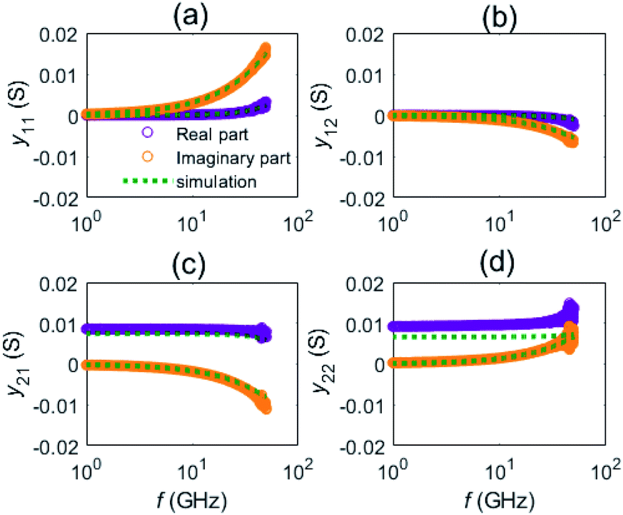 | ||
| Fig. 4 Measured (circles) and modelled (dotted lines) Y-parameters as a function of the frequency for a GFET biased at Vds = −1.1 V and Vgs = 0.5 V, corresponding to the highest measured fT,x = 34 GHz and fmax = 37 GHz. | ||
| Parameter | Optimized value |
|---|---|
| R g | 10 Ω |
| R s | 5.5 Ω |
| R d | 5.5 Ω |
| C pgs | 4.6 fF |
| C pgs | 7.6 fF |
Using the parasitic elements found in the previous step, we analyzed the bias dependence of fT,x and fmax. The results are compared with measurements in Fig. 5, showing similar trends. A more detailed insight on the bias dependence of RF performance can be obtained from the map of fmax shown in Fig. 6(a). A total of four maxima with fmax of ∼40 GHz are observed and labelled as A, B, C, and D, where A and C maxima occur at positive drain bias while B and D maxima at negative drain bias. Note that when gate voltage is equal to the Dirac voltage (i.e. Vgs = VD ≈ Vgs0 + Vds/2), transconductance gm changes its sign, which makes fmax ∼0. On top of that, for a given drain bias polarity, e.g. negative, the B maximum is located at Vgs < VD, which corresponds to a unipolar p-channel with the pinch-off close to the drain side, while at Vgs > VD, the D maximum corresponds to a unipolar n-channel with pinch-off close to the source side (see carrier distributions shown in Section S7 in the ESI†). Those maxima A, B, C and D are located at biases where there is a drop in the total carrier concentration close to the source or to the drain edges.
 | ||
| Fig. 5 Measured (squares) and modelled (solid lines) of (a) fT,x and (b) fmax as a function of the drain bias. Dashed lines represent fmax and fT,x switching off the self-heating effect. | ||
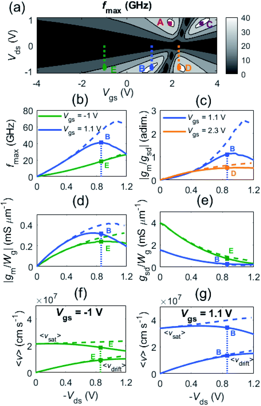 | ||
| Fig. 6 (a) Bias dependent fmax map. It presents four maxima labelled as A, B, C and D. Dashed lines represent the locus of considered drain bias points for fmax plot shown in (b) and |gm/gsd| plot in (c). Transconductance, gm, and output conductance, gsd, are represented in (d) and (e), respectively. (f) and (g) show average drift velocity and saturation velocity, respectively. Dashed lines correspond to the case where SHE have been switched off. | ||
It has been argued that the highest fmax needs current saturation in GFETs. To get the desired current saturation, it has been proposed that GFET operation close to the carrier velocity saturation regime is helpful.17,21,39,40 Here we critically review this idea by means of Fig. 6, which helps to visualize the connection between the drift velocity and the small-signal parameters (gm and gsd). Firstly, in Fig. 6(a) we have plotted the bias dependence of fmax, which displays four maxima. Notably, the bias locations of those maxima roughly coincide with the |gm| peaks (see Fig. S5 in the ESI†), so the |gm| maxima seem to be an adequate approximate rule to select the bias point if the intended FoM is fmax. However, there may be other options to choose the bias point depending on the targeted FoM, for instance, maximization of linearity, noise minimization, etc.
For a deeper insight in Fig. 6(a), we analyzed fmax evolution at two different constant Vgs, the first at Vgs = 1.1 V passing through the maximum B (dashed blue line), and the second at Vgs = −1.0 V (dashed green line) passing far away from the maximum B. The resulting plot is shown in Fig. 6(b). We chose bias B because it presents a higher voltage gain (ratio |gm/gsd|) than bias D, as can be seen in Fig. 6(c). GFETs tend to present very low voltage gains due to the relatively large values of gsd41–44 but in this work we show that this is not an obstacle to reach high power gain. For Vgs = 1.1 V case, the B maximum is reached at Vds = −0.86 V, while for Vgs = −1.0 V there is no an absolute maximum of fmax, being fmax a monotonous function of Vds, instead. Analyzing the average drift velocity in Fig. 6(f), we confirm the expectation that, far from the B maximum, the higher the drift velocity is (even approaching the saturation velocity), the better fmax and the current saturation are, as shown in Fig. 6(b) and (e), respectively. This behavior indeed happens for biases far away from the Dirac voltage, where the channel behaves as unipolar. However, the largest fmax is observed at biases near the crossover between unipolar and bipolar behavior such as the B point, where it does not hold that the highest drift velocity, represented in Fig. 6(g), gives the largest fmax, represented in Fig. 6(b). Fig. 6(d) and (e) show that a high value of gm together with a relatively low value of gsd, i.e. a high voltage gain, is needed to reach the highest fmax possible. The bias point B and the bias corresponding to the maximum of |gm| slightly differ because fmax depends in a complex way not only on gm, but on gsd, the transcapacitances and the parasitic elements.45
On the other hand, fmax is not the highest possible when the GFET is operated far away from Dirac voltage, and this can be explained by the degraded gm and gsd, as shown in Fig. 6(d) and (e), respectively. The degradation of gm and gsd at bias E respect to the bias B is caused, in turn, by a decrease in the drift velocity because of the larger carrier concentration. The bias that maximizes RF performance is thus the result of a complex interplay between carrier concentration and carrier velocity in graphene, where self-heating plays a significant role.
A local analysis of the carrier velocities along the channel at both biases E and B (Fig. 7) reveals more details on the central question of this paper, namely, if velocity saturation is needed for the highest fmax. As there are two transport mechanisms at play (drift and diffusion), we have introduced in S3 of the ESI,† as a matter of convenience, the definitions of drift, diffusion and total velocities that can be directly compared with the saturation velocity. At the E bias, where the channel is unipolar p-type, Fig. 7(d) shows that νdrift dominates over νdiff and is roughly 50% of νsat. The ratio νdrift/νsat could be increased up to ∼100% with a higher drain bias; for instance, it is 64% for Vds = −1.2 V, according to Fig. 6(f). However, at the B point, where the pinch-off is near the drain side, diffusion contribution is much higher with νdiff/νdrift around 40% near the drain, being νdrift/νsat ∼45%, as can be seen in Fig. 7(b). Therefore, our results do not support that operating in the regime of velocity saturation results in the highest fmax.
 | ||
| Fig. 7 Distribution along the channel of relevant parameters at bias points labelled as B and E in Fig. 6(a). Solid lines correspond simulations with activated SHE (T = 571 K at bias B and 723 K at bias E) and dashed lines to simulations switching off the SHE (T = 300 K). (a) Electron and hole concentration at bias B and (c) at bias E. (b) Saturation velocity and carrier velocity broken down into drift and diffusion velocities at bias B and (d) at bias E. | ||
To assess the impact of SHE, we have shown in Fig. 3(a) how SHE affects drain current, after switching it on and off in the simulations. It can be observed that current saturation is a result of self-heating, which is triggered at |Vds| > 0.6 V. Additionally, Fig. 5–7 also show the SHE impact on the different parameters of the GFET. At biases near maximum values of fmax, SHE are prominent and graphene temperature reaches ∼700 K. Importantly, Fig. 8 shows that SHE degrade the value of fmax from 65 to 40 GHz, mainly due to a decrease in vdrift, which reduces gm from 0.4 to 0.3 mS μm−1 despite the larger νdrift/νsat ratio. This way, it can be concluded that high temperatures limit the RF performance of GFETs. Pop's model for thermal resistance22,33 can estimate a reduction of up to 90% if the SiO2 was substituted by a material like sapphire, which exhibits a thermal conductivity 30 times higher. This would mean an increase in fmax to almost the level of SHE-free GFETs, according to Fig. 8 and assuming that all the power is dissipated through the substrate. More details on the impact of SHE on RF performance can be found in Section S9 of the ESI.†
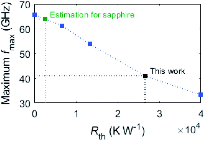 | ||
| Fig. 8 Maximum fmax as a function of the Rth. It has been calculated within the 3rd quadrant of the coordinate plane (Vgs–VD, Vds) with |Vds| < 1 V. Without SHE, fmax can reach 65 GHz. | ||
Conclusions
In this work we analyze the influence of carrier velocity saturation on the RF performance of GFETs by means of a drift–diffusion self-consistent simulator. The model includes a number of effects defining the current saturation, namely, the two-dimensional electrostatics, saturation velocity effects, and self-heating effects, which are especially relevant at short channels and/or large drain bias. First, we optimized the model parameters to fit the experimental DC characteristics of a prototype GFET. Then, the measured Y parameters were reproduced by fitting the values of the parasitic capacitances and the gate series resistance using the GFET small-signal equivalent circuit. We simulated the bias dependence of the measured RF FoMs and we discussed the role played by saturation velocity in defining the highest fmax. For biases far from the Dirac voltage, where the channel is unipolar and highly concentrated, a higher drift velocity results in a larger fmax. However, the largest fmax are located at biases close to the onset of bipolar conduction and far from the saturated velocity regime. In that scenario the pinch-off point is close to either the source or drain edge and drift velocity there is no longer saturated. This is caused by the combined effects of carrier concentration and total velocity, which are interdependent. Notably, we found a significant degradation of fmax at high drain biases because of the self-heating. Based on these results, further optimization of the GFET design for applications in advanced RF electronics can be done by selecting the appropriate bias and reducing the effects of self-heating.Authors contributions
D. J., J. S. and A. V. conceived the study. P. C. F. conducted the research. F. P. and P. C. F. developed the theoretical models. C. S., L. B., A. V., A. G. and X. Y. developed the technology. X. Y. and M. B. contributed on device fabrication. A. V., M. A. and M. B. characterized fabricated devices. D. J., J. S., A. V., M. A., M. B. and P. C. F. contributed on the analysis of results. C. S. and L. B. grew high-quality chemical-vapour-deposited graphene. D. N. and M. O. developed advanced technology and carried out the transfer of graphene onto Si substrate. D. J., A. V., M. B. and P. C. F. wrote the manuscript. J. S., A. G. and F. P. provided feedback on the manuscript drafts.Conflicts of interest
There are no conflicts to declare.Acknowledgements
This work was funded in part by the European Union's Horizon 2020 Research and Innovation Program under Grant GrapheneCore2 785219 and No. GrapheneCore3 881603, in part by the European Regional Development Funds (ERDR) allocated to the Programa Operatiu FEDER de Catalunya 2014–2020, with the support of the Secretaria d’Universitats i Recerca of the Departament d’Empresa I Coneixemment of the Generalitat de Catalunya for emerging technology clusters to carry out valorization and transfer of research results (reference of the GraphCAT project: 001-P001702). It has also been partially funded by the Ministerio de Economía y Competitividad under Grant TEC2015-67462-C2-1-R, in part by the Ministerio de Ciencia, Innovación y Universidades under grant RTI2018-097876-B-C21 (MCIU/AEI/FEDER, UE), in part in part by the Swedish Research Council under Grant No 2017-04504, and in part by the Academy of Finland.References
- K. Sengupta, T. Nagatsuma and D. M. Mittleman, Nat. Electron., 2018, 1, 622–635 CrossRef.
- F. Schwierz, J. Pezoldt and R. Granzner, Nanoscale, 2015, 7, 8261–8283 RSC.
- F. Schwierz, Proc. IEEE, 2013, 101, 1567–1584 CAS.
- H. Wang, A. Hsu and J. Kong, IEEE Trans. Electron Devices, 2011, 58, 1523–1533 Search PubMed.
- K. S. Novoselov, a K. Geim, S. V Morozov, D. Jiang, M. I. Katsnelson, I. V Grigorieva, S. V Dubonos and A. A. Firsov, Nature, 2005, 438, 197–200 CrossRef CAS PubMed.
- K. I. Bolotin, K. J. Sikes, J. Hone, H. L. Stormer and P. Kim, Phys. Rev. Lett., 2008, 101, 096802 CrossRef CAS PubMed.
- K. D. Holland, N. Paydavosi, N. Neophytou, D. Kienle and M. Vaidyanathan, IEEE Trans. Nanotechnol., 2013, 12, 566–577 CAS.
- F. Giubileo and A. Di Bartolomeo, Prog. Surf. Sci., 2017, 92, 143–175 CrossRef CAS.
- Z.-Y. Ong and M. V Fischetti, Phys. Rev. B, 2012, 86, 121409 CrossRef.
- S. Adam, E. H. Hwang, E. Rossi and S. Das Sarma, Solid State Commun., 2009, 149, 1072–1079 CrossRef CAS.
- Z.-Y. Ong and M. V Fischetti, Phys. Rev. B, 2013, 88, 045405 CrossRef.
- H. Lyu, Q. Lu, J. Liu, X. Wu, J. Zhang, J. Li, J. Niu, Z. Yu, H. Wu and H. Qian, Sci. Rep., 2016, 6, 35717 CrossRef CAS PubMed.
- J. S. Moon, H.-C. Seo, M. Antcliffe, D. Le, C. McGuire, A. Schmitz, L. O. Nyakiti, D. K. Gaskill, P. M. Campbell, K.-M. Lee and P. Asbeck, IEEE Electron Device Lett., 2013, 34, 465–467 CAS.
- E. Guerriero, P. Pedrinazzi, A. Mansouri, O. Habibpour, M. Winters, N. Rorsman, A. Behnam, E. A. Carrion, A. Pesquera, A. Centeno, A. Zurutuza, E. Pop, H. Zirath and R. Sordan, Sci. Rep., 2017, 7, 1–7 CrossRef CAS PubMed.
- I. Meric, C. R. Dean, S. J. Han, L. Wang, K. A. Jenkins, J. Hone and K. L. Shepard, Tech. Digest Int. Elect. Devices Meet., 2011, 2.1.1–2.1.4 Search PubMed.
- C. Yu, Z. Z. He, Q. B. Liu, X. B. Song, P. Xu, T. T. Han, J. Li, Z. H. Feng and S. J. Cai, IEEE Electron Device Lett., 2016, 37, 684–687 CAS.
- Z. Guo, R. Dong, P. S. Chakraborty, N. Lourenco, J. Palmer, Y. Hu, M. Ruan, J. Hankinson, J. Kunc, J. D. Cressler, C. Berger and W. A. De Heer, Nano Lett., 2013, 13, 942–947 CrossRef CAS PubMed.
- S. Rodriguez, S. Vaziri, A. Smith, S. Fregonese, M. Ostling, M. C. Lemme and A. Rusu, IEEE Trans. Electron Devices, 2014, 61, 1199–1206 Search PubMed.
- O. Habibpour, J. Vukusic and J. Stake, IEEE Trans. Electron Devices, 2012, 59, 968–975 CAS.
- G. I. Zebrev, A. A. Tselykovskiy, D. K. Batmanova and E. V. Melnik, IEEE Trans. Electron Devices, 2013, 60, 1799–1806 Search PubMed.
- I. Meric, M. Y. Han, A. F. Young, B. Ozyilmaz, P. Kim and K. L. Shepard, Nat. Nanotechnol., 2008, 3, 654–659 CrossRef CAS PubMed.
- S. V. Suryavanshi and E. Pop, J. Appl. Phys., 2016, 120, 224503 CrossRef.
- F. Pasadas and D. Jiménez, IEEE Trans. Electron Devices, 2016, 63, 2936–2941 CAS.
- P. C. Feijoo, D. Jiménez and X. Cartoixà, 2D Mater., 2016, 3, 025036 CrossRef.
- P. C. Feijoo, F. Pasadas, J. M. Iglesias, M. J. Martín, R. Rengel, C. Li, W. Kim, J. Riikonen, H. Lipsanen and D. Jiménez, Nanotechnology, 2017, 28, 485203 CrossRef PubMed.
- J. G. Champlain, J. Appl. Phys., 2011, 109, 084515 CrossRef.
- J. G. Champlain, Solid. State. Electron., 2012, 67, 53–62 CrossRef CAS.
- M. Bonmann, M. Asad, X. Yang, A. Generalov, A. Vorobiev, L. Banszerus, C. Stampfer, M. Otto, D. Neumaier and J. Stake, IEEE Electron Device Lett., 2019, 40, 131–134 CAS.
- Y. Wu, X. Zou, M. Sun, Z. Cao, X. Wang, S. Huo, J. Zhou, Y. Yang, X. Yu, Y. Kong, G. Yu, L. Liao and T. Chen, ACS Appl. Mater. Interfaces, 2016, 8, 25645–25649 CrossRef CAS PubMed.
- V. Passi and J.-P. Raskin, Semicond. Sci. Technol., 2017, 32, 123004 CrossRef.
- D. Kuylenstierna, M. Norling, A. Vorobiev, K. Reimann, D. Lederer, J. Raskin and S. Gevorgian, in 2007 IEEE/MTT-S International Microwave Symposium, IEEE, 2007, pp. 2055–2058 Search PubMed.
- M. Bonmann, A. Vorobiev, M. A. Andersson and J. Stake, Appl. Phys. Lett., 2017, 111, 233505 CrossRef.
- V. E. Dorgan, M.-H. Bae and E. Pop, Appl. Phys. Lett., 2010, 97, 082112 CrossRef.
- J. Chauhan and J. Guo, Appl. Phys. Lett., 2009, 95, 1–4 CrossRef.
- A. D. Liao, J. Z. Wu, X. Wang, K. Tahy, D. Jena, H. Dai and E. Pop, Phys. Rev. Lett., 2011, 106, 256801 CrossRef PubMed.
- Y. Tsividis and C. McAndrew, The MOS transistor, Oxford University Press, New York, 3rd edn, 2012 Search PubMed.
- P. C. Feijoo, F. Pasadas, J. M. Iglesias, E. M. Hamham, R. Rengel and D. Jimenez, IEEE Trans. Electron Devices, 2019, 66, 1567–1573 CAS.
- M. Bonmann, M. Krivic, X. Yang, A. Vorobiev, L. Banszerus, C. Stampfer, M. Otto, D. Neumaier and J. Stake, IEEE Trans. Electron Devices, 2020, 67, 1277–1284 Search PubMed.
- Q. Wilmart, M. Boukhicha, H. Graef, D. Mele, J. Palomo, M. Rosticher, T. Taniguchi, K. Watanabe, V. Bouchiat, E. Baudin, J. Berroir, E. Bocquillon, G. Fève, E. Pallecchi and B. Plaçais, Appl. Sci., 2020, 10, 446 CrossRef CAS.
- Z. H. Feng, C. Yu, J. Li, Q. B. Liu, Z. Z. He, X. B. Song, J. J. Wang and S. J. Cai, Carbon, 2014, 75, 249–254 CrossRef CAS.
- R. Grassi, A. Gnudi, V. Di Lecce, E. Gnani, S. Reggiani and G. Baccarani, IEEE Trans. Electron Devices, 2014, 61, 617–624 CAS.
- E. Guerriero, L. Polloni, L. G. Rizzi, M. Bianchi, G. Mondello and R. Sordan, Small, 2012, 8, 357–361 CrossRef CAS.
- S.-J. Han, K. A. Jenkins, A. Valdes Garcia, A. D. Franklin, A. A. Bol and W. Haensch, Nano Lett., 2011, 11, 3690–3693 CrossRef CAS PubMed.
- R. Grassi, A. Gnudi, V. Di Lecce, E. Gnani, S. Reggiani and G. Baccarani, Solid. State. Electron., 2014, 100, 54–60 CrossRef CAS.
- F. Pasadas, W. Wei, E. Pallecchi, H. Happy and D. Jimenez, IEEE Trans. Electron Devices, 2017, 64, 4715–4723 CAS.
Footnote |
| † Electronic supplementary information (ESI) available: Section S1 details fabrication and characterization of graphene devices used in this work. Then, Sections S2 and S3 present the mathematical modelling for the simulation of the DC characteristics of GFETs and calculation of carrier velocity in graphene. Experimental and simulated transfer characteristics of GFETs are represented in Section S4. Next, Section S5 includes the mathematical expressions used to extract small-signal parameter and RF performance from the simulated DC characteristics. Section S6 presents the measurements of the parasitic capacitances of the GFET. Section S7 shows the carrier concentration distribution at biases where the magnitude of transconductance is maximized. Section S8 delves deep into the effect of interface traps on GFET characteristics and RF performance. Finally, Section S9 investigates the RF performance degradation caused by self-heating. See DOI: 10.1039/c9na00733d |
| This journal is © The Royal Society of Chemistry 2020 |