
 Open Access Article
 This Open Access Article is licensed under a
 Creative Commons Attribution 3.0 Unported Licence
Many-body effects in an MXene Ti2CO2 monolayer modified by tensile strain: GW-BSE calculations†
Yi-min
Ding
a,
Xiaomin
Nie
a,
Huilong
Dong
 b,
Nopporn
Rujisamphan
c and
Youyong
Li
*a
b,
Nopporn
Rujisamphan
c and
Youyong
Li
*a
aInstitute of Functional Nano & Solf Materials (FUNSOM), Jiangsu Key Laboratory for Carbon-Based Functional Materials & Devices, Soochow University, Suzhou, Jiangsu 215123, China. E-mail: yyli@suda.edu.cn
bSchool of Chemistry and Materials Engineering, Changshu Institute of Technology, Changshu, Jiangsu 215500, China
cKing Mongkut's University of Technology Thonburi (KMUTT), 126 Pracha Uthit Road, Bang Mod, Thung Khru, Bangkok 10140, Thailand
First published on 6th May 2020
Abstract
MXenes, two-dimensional (2D) layered transition metal carbide/nitride materials with a lot of advantages including high carrier mobility, tunable band gap, favorable mechanical properties and excellent structural stability, have attracted research interest worldwide. It is imperative to accurately understand their electronic and optical properties. Here, the electronic and optical response properties of a Ti2CO2 monolayer, a typical member of MXenes, are investigated on the basis of first-principles calculations including many-body effects. Our results show that the pristine Ti2CO2 monolayer displays an indirect quasi-particle (QP) band gap of 1.32 eV with the conduction band minimum (CBM) located at the M point and valence band maximum (VBM) located at the Γ point. The optical band gap and binding energy of the first bright exciton are calculated to be 1.26 eV and 0.56 eV, respectively. Under biaxial tensile strains, the lowest unoccupied band at the Γ point shifts downward, while the lowest unoccupied band at the M point shifts upward. Then, a direct band gap appears at the Γ point in 6%-strained Ti2CO2. Moreover, the optical band gap and binding energy of the first bright exciton decrease continuously with the increase of the strain due to the increase of the lattice parameter and the expansion of the exciton wave function. More importantly, the absorbed photon flux of Ti2CO2 is calculated to be 1.76–1.67 mA cm−2 with the variation of the strain, suggesting good sunlight optical absorbance. Our work demonstrates that Ti2CO2, as well as other MXenes, hold untapped potential for photo-detection and photovoltaic applications.
Introduction
As a new member of the two-dimensional (2D) material family, MXenes, layered transition metal carbide/nitride materials, have aroused the interest of a great number of researchers, due to their advantages including high carrier mobility, tunable band gap, favorable mechanical properties and excellent structural stability.1–4 The first member of MXenes, Ti3C2Tx nanosheets, was produced by the room temperature exfoliation of Ti3AlC2 in hydrofluoric acid.5 After this, more than 20 kinds of MXenes have been successfully synthesized and dozens of hundreds of new MXenes have been theoretically simulated.6In principle, 2D MXenes can be denoted as Mn+1XnTx (n = 1, 2 and 3), in which M is a transition metal (TM), X is nitrogen and/or carbon and Tx represents surface functional groups (i.e. –F, –O, or –OH). The flexible tunability of the elemental composition of MXenes leads to plenty of unique physical and chemical properties, which makes them suitable for numerous applications, such as electrodes of lithium/sodium-ion batteries, electrochemical catalysts, supercapacitors, hydrogen storage materials, molecular sensors, and antibacterial and bioimaging probe materials.2,4,7 Unfortunately, most MXenes have exhibited excellent metallic conductivity without an intrinsic bandgap, which limits their applications in laser diode (LD), field-effect transistor (FET), and light emitting diode (LED) devices.
Recently, great efforts have been made to find semiconducting MXenes. It is predicted that Sc2CF2, Sc2CO2, Ti2CO2, Zr2CO2 and Hf2CO2 have an indirect band gap, and only Sc2COH2 has a direct band gap of 0.45 eV.8 What is noteworthy is that the thermoelectric performance and elastic and optical properties of MXenes are highly dependent on the surface terminated groups Tx.9,10 Recently, a two transition metal MXene Mo2TiC2O2 was found to be a 2D topological semiconductor with a band gap of 0.17 eV.11 For the first time, Lai et al. studied the transport properties of 2D Ti2CTx FETs and obtained a high carrier mobility of 104 cm2 V−1 s−1.12 They estimated an energy gap of 80 meV for Ti2CTx, where the functional group Tx is difficult to determine quantificationally due to the chemical exfoliation processes. Zhang et al. demonstrated that the carrier mobility of a Ti2CO2 monolayer reaches 102 and 104 cm2 V−1 s−1 for electrons and holes, respectively, and its indirect band gap is 0.91 eV on the basis of density functional theory calculations.13 Moreover, the band structures of Ti2CO2 can be tuned effectively by strain, and an indirect to direct band gap transition in Ti2CO2 was found under a tensile strain of 4%.14 With the increase of compressive strains, Ti2CO2 undergoes a transition from an indirect bandgap semiconductor to a metal.15 Accurate GW quasiparticle calculations show that the Ti2CO2 monolayer has an indirect bandgap of 1.15 eV, much larger than that found by density functional theory calculations.16 It is well known that excitonic effects have a crucial impact on the electronic and optical response of 2D materials caused by the incomplete dielectric screening and strong quantum confinement.17,18 However, there have been few reports on the excitonic properties of MXenes until now, which are vital for the development of MXene-based electronic and optical devices.
Herein, we aim to study the electronic and optical properties including excitonic effects of MXenes, taking the Ti2CO2 monolayer as an example, on the basis of many-body perturbation theory, i.e. Green's function (GW) plus Bethe–Salpeter equation (GW-BSE) calculations. The semiconducting characteristics of the Ti2CO2 monolayer have been confirmed not only by theoretical studies but also by experimental work,12,16 while the other semiconducting MXene materials have only been predicted by theoretical simulations.8–10 Our results reveal that the first bright exciton peak of the Ti2CO2 monolayer is located at 1.26 eV with an exciton binding energy as large as 0.54 eV. Under a biaxial tensile strain of 6%, the Ti2CO2 monolayer transforms into a direct bandgap semiconductor with the band gap increased to 1.59 eV at the Γ point. With the increase of strain, the excitation energy of the first bright exciton and binding energies decrease. And the absorbed photon flux of Ti2CO2 is calculated to be 1.76 mA cm−2, suggesting good sunlight optical absorbance.
Computational methods and details
Firstly, the electronic ground states of the Ti2CO2 monolayer were calculated based on density functional theory (DFT) in the generalized gradient approximation (GGA) implemented in the QUANTUM ESPRESSO package.19 The optimized norm conserving Vanderbilt pseudopotentials with the Perdew–Burke–Ernzerhof (PBE) functional were employed with a plane-wave cutoff energy set at 100 Ry.20 The first Brillouin zone (BZ) was sampled using Monkhorst–Pack k-mesh of 15 × 15 × 1. The total energy and the atomic forces were converged within 10−4 eV and 0.01 eV Å−1, respectively, after structural optimization. The vacuum spacing was set at 15 Å to avoid any unnecessary interaction between adjacent layers. Furthermore, the magnitude of the in-plane strain was calculated using δ = (a −a0)/a0 × 100%, where a0 and a are the calculated pristine and strained lattice parameters. It should be pointed out that the structures of Ti2CO2 almost remain unchanged under the applied strains (from 0% to 6%). This simulation method of applying strains has been carried out on 2D materials and resulted in reasonable conclusions.14,21As we all know, DFT in the formulation of Kohn and Sham is a ground-state theory in the form of an effective one-particle Schrödinger equation (the Kohn–Sham equation), which results in semiconductor bandgap underestimation problems and discrepancies between the calculated and experimental spectra.22 In order to overcome these problems, the excited states of real systems have to be calculated correctly. Many-body perturbation theory, a GW approach based on a set of Green's-function equations, has been successfully used to describe excited state properties and obtain more accurate band gaps.23 Furthermore, by solving the Bethe–Salpeter equation (BSE), the electron–hole interactions are well described, and the discrepancies between the calculated and experimental spectra could be eliminated.24,25 In brief, the GW-BSE approach, based on many-body perturbation theory, has been used widely to calculate the accurate band gap and absorption spectra. It can be used not only in simple systems but also in large systems such as Si supercells containing 1726 Si atoms.26 Considering the huge computational costs, researchers prefer to study simpler systems by GW-BSE approaches, such as small molecules, pristine 2D materials (InSe, MoS2, and black phosphorus) and graphene quantum dots.18,27–29
Our GW-BSE calculations were carried out within the BerkeleyGW code.23,30,31 The one-shot GW calculation was performed to obtain the quasi-particle (QP) bandstructure. The dynamical screening effects were included using the Hybertsen–Louie generalized plasmon pole (HL-GPP) model.31 Following the Nonuniform Neck Subsampling (NNS) method, the dielectric matrix was calculated on a 12 × 12 × 1 uniform q grid with an additional 10 q-points in the small-q region, which provides an efficient way to capture specific features of the dielectric matrix in 2D materials due to the electronic confinement.32 The dielectric matrix included plane-wave components up to 30 Ry, and about 1000 unoccupied states were included in the calculation of both the polarization and GW self-energy. Furthermore, the static remainder correction was added to the self-energy to speed up convergence with respect to summation over unoccupied states, and a truncated Coulomb interaction was used to prevent spurious interactions between periodic images.33,34 These parameters converged the QP gaps at Γ and M to better than 0.02 eV. The BSE matrix elements were calculated on a uniform 12 × 12 × 1 k grid and then interpolated to a 64 × 64 × 1 fine k grid using the Clustered Sampling Interpolation (CSI) technique.32 In CSI, BSE matrix elements are explicitly calculated for 4 additional k points in each cluster, sampled along the (100) direction. Six valence bands and three conduction bands were set to describe the excitons and to obtain the optical absorption spectra. These converged the BSE eigenvalues to better than 0.05 eV.
Results and discussion
As shown in Fig. 1, the Ti2CO2 monolayer consists of five atomic layers with a hexagonal unit cell, where the C layer is sandwiched between two Ti and two O layers. It has been confirmed to be the most stable structure of Ti2CO2 in previous studies.8,35 After structural relaxation, an equilibrium lattice constant of 3.03 Å for the pristine Ti2CO2 monolayer is obtained, which is consistent with that in previous theoretical studies (3.04/3.01 Å).14,15 Next, the band structures and projected density of states (PDOS) are calculated by the GGA method. From Fig. 2(a)–(c), we know that the Ti2CO2 monolayer has an indirect band gap of 0.32 eV, and the conduction band minimum (CBM) and valence band maximum (VBM) are located at the M and Γ point, respectively. Furthermore, the VBM of Ti2CO2 is mainly made up of C-2p and O-2p states, and the CBM is mainly made up of Ti-3d and O-2p states. Accordingly, the partial charge density of the VBM is distributed around C and O atoms, while the charge density of the VBM is distributed around Ti and O atoms. These results are consistent with previous calculations.14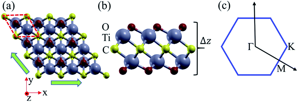 | ||
| Fig. 1 (a) Top and (b) side view of the crystal structure of the Ti2CO2 monolayer, and the shape of the Brillouin zone (c). Here the green arrows show the directions of the in-plane biaxial strains, and Δz represents the out-plane thickness. | ||
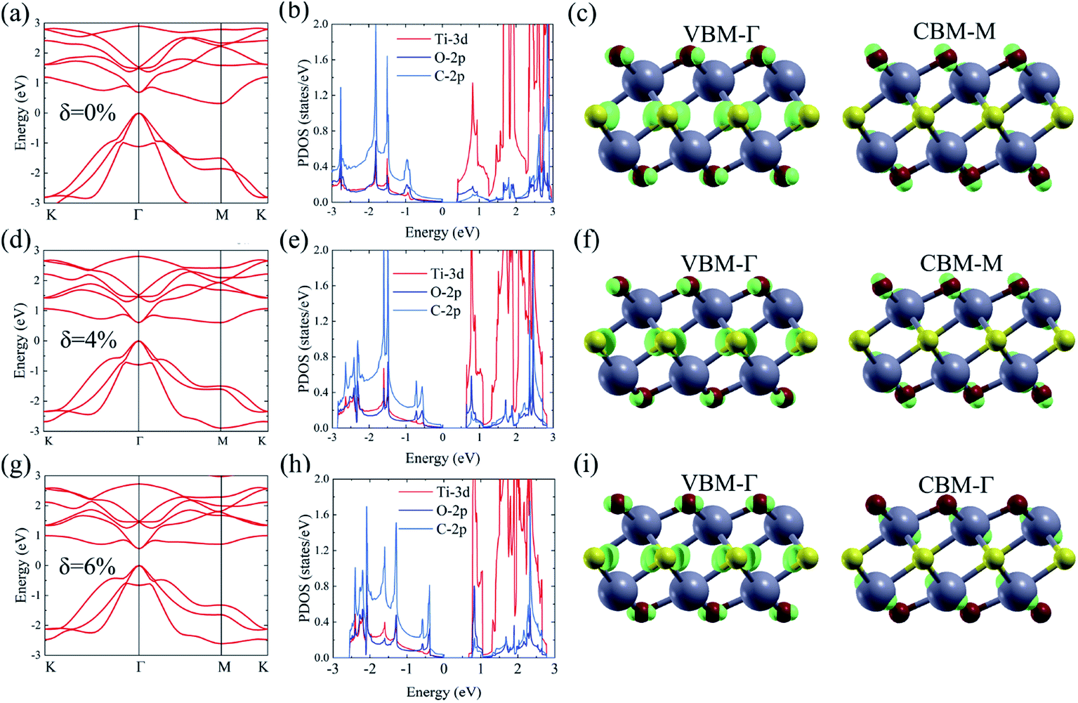 | ||
| Fig. 2 Calculated band structure, PDOS, and partial charge density of the CBM and VBM of the Ti2CO2 monolayer based on GGA calculations under strain, δ = 0% (a–c), 4% (d–f) and 6% (g–i), respectively. | ||
In general, indirect bandgap semiconductors are not efficient light emitters because a phonon with a high momentum is required to transfer an electron from the conduction band to the valence band.36 In order to improve the light emitting probability of the Ti2CO2 monolayer, we modified the electronic properties by applying in-plane biaxial strains. Fig. 3 shows the Γ to Γ and Γ to M band gap variations with the biaxial strains. With the increase of the strain from −4% to 8%, the Γ to Γ band gap values decrease continuously, and the Γ to M band gap values increase continuously. Two transition points are found. Under a compressive strain of δ = −4%, the direct band gap decreases to zero, leading to metallic properties in the Ti2CO2 monolayer. Under a tensile strain of δ = 4%, indirect–direct band gap transition is found. The direct band gap is very beneficial for light absorption and emission in semiconductors. Thus, we choose two strain values of δ = 4% and 6% before and after the indirect–direct bandgap transition point as representative situations and discuss their effects on the electronic and optical properties of the Ti2CO2 monolayer in detail.
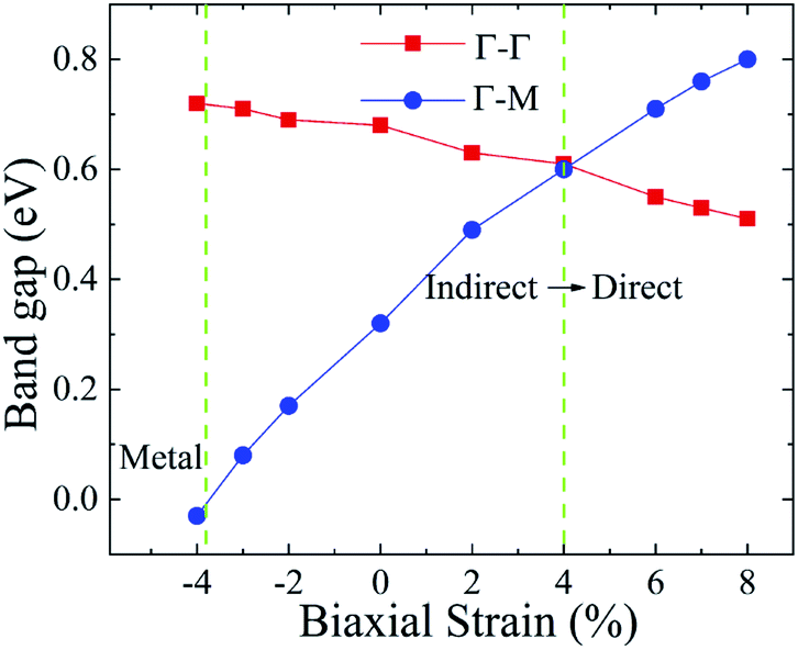 | ||
| Fig. 3 The Γ to Γ and Γ to M band gap values dependent on the various biaxial strains from −4% to 8%. | ||
Under a tensile strain of δ = 4%, the Ti2CO2 monolayer still exhibits an indirect band gap, which increases to 0.60 eV, with the VBM and CBM located at the Γ and M point, respectively, as presented in Fig. 2(d)–(f). Interestingly, Ti2CO2 becomes a direct bandgap semiconductor with both the CBM and VBM located at the Γ point under 6% strain, and the band gap decreases to 0.55 eV. Similar to that of pristine Ti2CO2, the VBM of strained Ti2CO2 is also made up of C-2p and O-2p states. Different from pristine Ti2CO2, the CBM of 6%-strained Ti2CO2 is only made up of the Ti-3d state with charge density distributed only around Ti atoms, as presented in Fig. 2(g)–(i). This is because the CBM has been shifted to the Γ point instead of the M point. As shown in Fig. 1(a), under in-plane tensile strains, the in-plane lattice is extended within the xy-plane. After the relaxation of atom positions, the material thickness Δz, perpendicular to the xy-plane, decreases a little, which can be understood to be the Poisson effect. The distance between O and Ti/C atoms is reduced a little, which results in enhanced O–Ti/C interactions. Thus, the contribution of O in the CBM is significantly increased with the applied strain. Considering the bandgap underestimation problem in the usual DFT-GGA methods, we further carry out GW calculations to obtain accurate quasiparticle bandstructures of pristine and strained Ti2CO2 monolayers.
The many-body effects, namely the electron–electron and electron–hole interactions for quasiparticles and optical excitations, can be well-described by the GW-BSE method, which gives results in good agreement with the experimental band gap and optical spectra, particularly in 2D materials.18 In GW approximation, the many-electron self-energy operator Σ, containing the effect of exchange and correlation among the electrons, was used to replace the exchange–correlation potential Vxc in DFT.23 The incorporation of many-body self-energy corrections results in more accurate QP energies and increased bandgap values. According to Fig. 4, the pristine Ti2CO2 monolayer still displays an indirect G0W0 band gap with the value increased to 1.32 eV (1 eV larger than that calculated by the DFT method), while the VBM and CBM are located at the Γ and M point, respectively. From the point of view of physics, the increase of the band gap is attributed to the incomplete dielectric screening and strong quantum confinement effect in suspended 2D materials.37,38 Under a tensile strain of δ = 4%, the Ti2CO2 monolayer also displays an indirect band gap of 1.59 eV, while the direct bandgap at Γ is 1.67 eV. For δ = 6%, Ti2CO2 transforms into a direct bandgap semiconductor with a band gap of 1.59 eV at Γ, lower than the indirect energy gap of 1.68 eV between Γ and M. In brief, Ti2CO2 can be transformed into a direct band gap semiconductor by tensile strain.
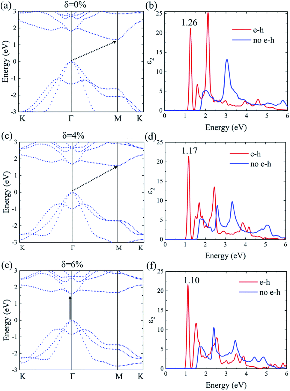 | ||
| Fig. 4 The G0W0 band structure and the imaginary part of the dielectric functions ε2 with and without e–h interactions of the Ti2CO2 monolayer under strain δ = 0% (a and b), 4% (c and d) and 6% (e and f), respectively. | ||
The evolutions of band gaps and band offsets of Ti2CO2 under strain are shown in Table 1 and Fig. 5. We can see that the energy level of the VBM at Γ moves up continuously under tensile strain. For the lowest conduction band, the energy level at Γ moves down, while the energy level at M moves up under strain. Finally, the energy level at Γ becomes lower than that at M, and thus a direct bandgap appears in Ti2CO2 at δ = 6%. In our calculations, the 6% tensile strain will lead to an obvious increase (0.18 Å) of the in-plane lattice constant and decrease of material thickness accordingly, which results in an upward shift of the lowest conduction band at M. The conduction-band inversion in the Ti2CO2 monolayer is thus induced by the tensile strain. Moreover, the GW method can accurately calculate the electron ionization and affinity potential and the energy difference of the VBM and CBM with respect to the vacuum level, respectively, as shown in Fig. 5. Under strain, both the affinity and ionization potential decrease from 5.63 to 5.12 eV and 6.95 to 6.71 eV, respectively. The decrease of the band gap and affinity and ionization potential of Ti2CO2 would result in enhanced photo-response.
| E g(GGA) | E g(GW) | E opt | E b | |||
|---|---|---|---|---|---|---|
| Γ–Γ | Γ–M | Γ–Γ | Γ–M | |||
| 0% | 0.68 | 0.32 | 1.82 | 1.32 | 1.26 | 0.56 |
| 4% | 0.61 | 0.60 | 1.67 | 1.59 | 1.17 | 0.50 |
| 6% | 0.55 | 0.71 | 1.59 | 1.68 | 1.10 | 0.49 |
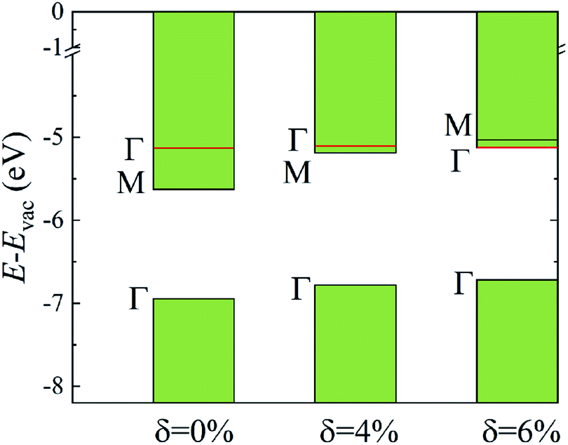 | ||
| Fig. 5 The calculated CBM and VBM alignment, relative to the vacuum level, for the different strain values. The shift of the energy level at Γ and M caused by strain is shown. | ||
The incorporation of the many-body effect has direct impacts not only on the correction of bandgaps but also on the optical spectra. The inclusion of electron–hole (e–h) interactions is essential for the calculation of optical spectra of 2D materials due to the reduced dimensionality and depressed screening. The enhanced excitonic effects caused by strong e–h interactions substantially reshape the optical spectra of 2D materials.28 Then, the imaginary part of the dielectric functions ε2, closely related to the absorbance spectra, is calculated with and without e–h interactions. From Fig. 4(b), (d) and (f), the absorption spectra calculated with e–h interactions have a redshift with respect to those calculated without e–h interactions. Thus, the main optical features are determined by bound excitonic states. The first absorption peak of the Ti2CO2 monolayer is located at 1.26 eV, which corresponds to the first bright exciton peak and is much smaller than the fundamental bandgap value from the calculation without e–h. Under strains of δ = 4% and 6%, the first bright exciton peak decreases to 1.17 and 1.10 eV, respectively, because of the reduction of the QP band gap at Γ. Fig. 6 shows the real-space and k-space distribution of the squared amplitude of first bright exciton wave functions. We can see that the main contributions for the first exciton peak are from the transitions between the highest valence and the lowest conduction bands close to the Γ point. In real space, the spatial distribution of the first bright exciton becomes more expanded under strain. The binding energy of an exciton is defined as the difference between the exciton's energy and the energy of the dominant band-to-band transition at Γ, where the lowest energy direct transition occurs.39 The binding energy of 0%, 4% and 6%-strained Ti2CO2 is 0.56, 0.50 and 0.49 eV, respectively. The decrease of binding energy is attributed to the extension of the exciton radius in real space caused by tensile strain, which results in reduced electron–hole interactions.
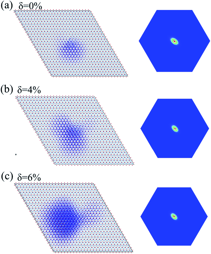 | ||
| Fig. 6 Exciton wave function for the lowest energy exciton in real space and k-space of the Ti2CO2 monolayer under strains of δ = 0% (a), 4% (b) and 6% (c), respectively. | ||
The first bright exciton peak of the Ti2CO2 monolayer is located at 1.26 eV (985 nm), which means Ti2CO2 has good potential for infrared detection and photovoltaic applications. In order to quantify the sunlight absorption of Ti2CO2, we further calculate the absorbed photon flux Jabs using40,41
 | (1) |
 | (2) |
What's more, Jabs is expressed as the upper-limit short-circuit electrical current density (units of mA cm−2) in the ideal case where every photon is converted to a carrier extracted from light-absorbing materials. The absorbed photon flux Jabs is calculated to be 1.76, 1.74 and 1.67 mA cm−2 for 0%, 4% and 6%-strained Ti2CO2, respectively. The slight reduction of Jabs can be attributed to the compression of the out-plane thickness Δz caused by the in-plane tensile strain. Most importantly, the calculated Jabs is much larger than that in 1 nm thick layers of Si (0.1), GaAs (0.3) and P3HT polymer (0.2),40 which suggests that Ti2CO2 shows great potential in photo-detection and photovoltaic applications.
Conclusions
In conclusion, we have studied the electronic properties and optical response of the Ti2CO2 monolayer with and without tensile strain using first-principles calculations based on the GW-BSE formalism. Due to incomplete dielectric screening and quantum confinement in suspended 2D materials, the indirect QP band gap of the pristine Ti2CO2 monolayer is increased to 1.32 eV, 1 eV larger than that by GGA calculation. With the increase of tensile strain, the lowest conduction band at the Γ point shifts downward, while the lowest conduction band at the M point shifts upward. Then, a conduction-band inversion occurs, which results in a direct band gap at the Γ point in 6%-strained Ti2CO2. The optical band gap is 1.26, 1.17 and 1.10 eV, and the binding energy of the first bright exciton is 0.56, 0.50 and 0.49 eV for the 0%-, 4%- and 6%-strained Ti2CO2 monolayer, respectively. Moreover, the absorbed photon flux Jabs of Ti2CO2 without and with strain is calculated to be 1.76–1.67 mA cm−2, suggesting enhanced sunlight optical absorbance. Our study reveals the huge potential of Ti2CO2 in photo-detection and photovoltaics devices.Conflicts of interest
There are no conflicts to declare.Acknowledgements
This work was supported by the National Natural Science Foundation of China (Grant No. 51761145013, 21703145, and 21673149), the National Key R & D Program of China (Grant No. 2017YFB0701600 and 2017YFA0204800), the 111 Project, the Joint International Research Laboratory of Carbon-Based Functional Materials and Devices, the Priority Academic Program Development of Jiangsu Higher Education Institutions (PAPD) and the Collaborative Innovation Center of Suzhou Nano Science & Technology.References
- M. Naguib, V. N. Mochalin, M. W. Barsoum and Y. Gogotsi, Adv. Mater., 2014, 24, 992–1005 CrossRef PubMed.
- H. Wang, Y. Wu, X. Yuan, G. Zeng, J. Zhou, X. Wang and J. W. Chew, Adv. Mater., 2018, 30, 1704561 CrossRef PubMed.
- Z. Li and Y. Wu, Small, 2019, 15, 1804736 CrossRef PubMed.
- J. Pang, R. G. Mendes, A. Bachmatiuk, L. Zhao, H. Q. Ta, T. Gemming, H. Liu, Z. Liu and M. H. Rummeli, Chem. Soc. Rev., 2019, 48, 72–133 RSC.
- M. Naguib, M. Kurtoglu, V. Presser, J. Lu, J. Niu, M. Heon, L. Hultman, Y. Gogotsi and M. W. Barsoum, Adv. Mater., 2011, 23, 4248–4253 CrossRef CAS PubMed.
- A. C. Rajan, A. Mishra, S. Satsangi, R. Vaish, H. Mizuseki, K.-R. Lee and A. K. Singh, Chem. Mater., 2018, 30, 4031–4038 CrossRef CAS.
- K. Huang, Z. Li, J. Lin, G. Han and P. Huang, Chem. Soc. Rev., 2018, 47, 5109–5124 RSC.
- M. Khazaei, M. Arai, T. Sasaki, C.-Y. Chung, N. S. Venkataramanan, M. Estili, Y. Sakka and Y. Kawazoe, Adv. Funct. Mater., 2013, 23, 2185–2192 CrossRef CAS.
- A. N. Gandi, H. N. Alshareef and U. Schwingenschlögl, Chem. Mater., 2016, 28, 1647–1652 CrossRef CAS.
- Y. Bai, K. Zhou, N. Srikanth, J. H. L. Pang, X. Heb and R. Wang, RSC Adv., 2016, 6, 35731–35739 RSC.
- L. Li, Comput. Mater. Sci., 2016, 124, 8–14 CrossRef CAS.
- S. Lai, J. Jeon, S. K. Jang, J. Xu, Y. J. Choi, J.-H. Park, E. Hwang and S. Lee, Nanoscale, 2015, 7, 19390–19396 RSC.
- X. Zhang, X. Zhao, D. Wu, Y. Jing and Z. Zhou, Nanoscale, 2015, 7, 16020–16025 RSC.
- X.-F. Yu, J.-B. Cheng, Z.-B. Liu, Q.-Z. Li, W.-Z. Li, X. Yang and B. Xiao, RSC Adv., 2015, 5, 30438–30444 RSC.
- S. A. Khan, B. Amin, L.-Y. Gan and I. Ahmad, Phys. Chem. Chem. Phys., 2017, 19, 14738–14744 RSC.
- Y. Zhang, W. Xia, Y. Wu and P. Zhang, Nanoscale, 2019, 11, 3993–4000 RSC.
- L. Yang, J. Deslippe, C.-H. Park, M. L. Cohen and S. G. Louie, Phys. Rev. Lett., 2009, 103, 186802 CrossRef PubMed.
- D. Y. Qiu, F. H. da Jornada and S. G. Louie, Phys. Rev. B, 2016, 93, 235435 CrossRef.
- P. Giannozzi, S. Baroni, N. Bonini, M. Calandra, R. Car, C. Cavazzoni, D. Ceresoli, G. L. Chiarotti, M. Cococcioni and I. Dabo, et al. , J. Phys.: Condens. Matter, 2009, 21, 395502 CrossRef PubMed.
- D. R. Hamann, Phys. Rev. B: Condens. Matter Mater. Phys., 2013, 88, 085117 CrossRef.
- M. Wu, J.-J. Shi, M. Zhang, Y.-M. Ding, H. Wang, Y.-L. Cen and J. Lu, Nanoscale, 2018, 10, 11441–11451 RSC.
- G. Onida, L. Reining and R. Rubio, Rev. Mod. Phys., 2002, 74, 601–659 CrossRef CAS.
- M. S. Hybertsen and S. G. Louie, Phys. Rev. B: Condens. Matter Mater. Phys., 1986, 34, 5390–5413 CrossRef CAS PubMed.
- M. Rohlfing and S. G. Louie, Phys. Rev. Lett., 1998, 81, 2312–2315 CrossRef CAS.
- S. Albrecht, L. Reining, R. Del Sole and G. Onida, Phys. Rev. Lett., 1998, 80, 4510–4513 CrossRef CAS.
- M. J. Ben, F. H. Jornada, A. Canning, N. Wichmann, K. Raman, R. Sasanka, C. Yang, S. G. Louie and J. Deslippe, Comput. Phys. Commun., 2019, 235, 187–195 CrossRef.
- M. J. van Setten, F. Caruso, S. Sharifzadeh, X. Ren, M. Scheffler, F. Liu, J. Lischner, L. Lin, J. R. Deslippe, S. G. Louie, C. Yang, F. Weigend, J. B. Neaton, F. Evers and P. Rinke, J. Chem. Theory Comput., 2015, 11, 5665–5687 CrossRef CAS PubMed.
- V. Tran, R. Soklaski, Y. Liang and L. Yang, Phys. Rev. B: Condens. Matter Mater. Phys., 2014, 89, 235319 CrossRef.
- P. Huang, J.-J. Shi, M. Zhang, X.-H. Jiang, H.-X. Zhong, Y.-M. Ding, X. Cao, M. Wu and J. Lu, J. Phys. Chem. Lett., 2016, 7, 2888–2892 CrossRef CAS PubMed.
- J. Deslippe, G. Samsonidze, D. A. Strubbe, M. Jain, M. L. Cohen and S. G. Louie, Comput. Phys. Commun., 2012, 183, 1269–1289 CrossRef CAS.
- M. Rohlfing and S. G. Louie, Phys. Rev. B: Condens. Matter Mater. Phys., 2010, 62, 4927–4944 CrossRef.
- F. H. da Jornada, D. Y. Qiu and S. G. Louie, Phys. Rev. B, 2017, 95, 035109 CrossRef.
- J. Deslippe, G. Samsonidze, M. Jain, M. L. Cohen and S. G. Louie, Phys. Rev. B, 2017, 87, 165124 CrossRef.
- S. Ismail-Beigi, Phys. Rev. B: Condens. Matter Mater. Phys., 2006, 73, 233103 CrossRef.
- L. Hong, R. F. Klie and S. Öğüt, Phys. Rev. B, 2016, 93, 115412 CrossRef.
- J. M. Escalante and A. Martinez, Phys. B, 2012, 407, 2044–2049 CrossRef CAS.
- C. D. Spataru, S. Ismail-Beigi, L. X. Benedict and S. G. Louie, Phys. Rev. Lett., 2004, 92, 077402 CrossRef PubMed.
- D. Y. Qiu, F. H. da Jornada and S. G. Louie, Phys. Rev. Lett., 2013, 111, 216805 CrossRef PubMed.
- G. Antonius, D. Y. Qiu and S. G. Louie, Nano Lett., 2018, 18, 1925–1929 CrossRef CAS PubMed.
- M. Bernardi, M. Palummo and J. C. Grossman, Nano Lett., 2013, 13, 3664–3670 CrossRef CAS PubMed.
- H. Dong, L. Zhou, T. Frauenheim, T. Hou, S.-T. Lee and Y. Li, Nanoscale, 2016, 8, 6994–6999 RSC.
Footnote |
| † Electronic supplementary information (ESI) available. See DOI: 10.1039/c9na00632j |
| This journal is © The Royal Society of Chemistry 2020 |