
 Open Access Article
 This Open Access Article is licensed under a Creative Commons Attribution-Non Commercial 3.0 Unported Licence
Improvement in hole transporting ability and device performance of quantum dot light emitting diodes†
Pei-Chieh
Chiu
and
Sheng-Hsiung
Yang
 *
*
Institute of Lighting and Energy Photonics, College of Photonics, National Chiao Tung University, No. 301, Gaofa 3rd Road, Guiren District, Tainan City 71150, Taiwan, Republic of China. E-mail: yangsh@mail.nctu.edu.tw; Fax: +886-6-3032535; Tel: +886-6-3032121 ext. 57895
First published on 21st November 2019
Abstract
In this research, we demonstrate a novel approach to improve the device performance of quantum dot light emitting diodes (QLEDs) by blending an additive BYK-P105 with poly(3,4-ethylenedioxythiophene):polystyrene sulfonate (PEDOT:PSS) as the hole transport layer. In addition, for the first time, polyethylenimine ethoxylated (PEIE)-modified zinc oxide nanoparticles (ZnO NPs) as the electron transport layer were applied in regular-type QLEDs for achieving high device efficiency. A very high brightness of 139![[thin space (1/6-em)]](https://www.rsc.org/images/entities/char_2009.gif) 909 cd m−2 and current efficiency of 27.2 cd A−1 were obtained for the optimized device with the configuration of ITO/PEDOT:PSS + BYK-P105/PVK/CdSe QDs/ZnO NPs/PEIE/LiF/Al that shows promising use in light-emitting applications.
909 cd m−2 and current efficiency of 27.2 cd A−1 were obtained for the optimized device with the configuration of ITO/PEDOT:PSS + BYK-P105/PVK/CdSe QDs/ZnO NPs/PEIE/LiF/Al that shows promising use in light-emitting applications.
1. Introduction
Colloidal quantum dots (QDs) and the corresponding light emitting diodes (QLEDs) are extensively investigated and considered as promising candidates for displays because of their unique optical properties, including color tunability, narrow emission bandwidth and high brightness. In the past few years, several research groups have demonstrated various lighting-emitting diodes using colloidal QDs as the emitting layers.1–5 The existing QLED structure is the same as that of general organic light emitting diodes which are fabricated via the solution process with the configuration of the hole transporting layer (HTL)/active layer/electron transporting layer (ETL). In terms of electrical and optical characteristics, good carrier transport capability and high transmittance must be considered. Electron-dominating metal oxides are gradually utilized as the ETL in various types of optoelectronic devices due to their chemical stability, convenient fabrication process and low sensitivity to moisture.6–9 Zinc oxide (ZnO) is considered to be the most promising material for QLEDs as it has high electron mobility and high transmittance in the visible range.8–10 ZnO thin films are commonly prepared by the sol–gel method11−13 and need to be calcined over 400 °C to promote crystallinity and remove organic residues.14 It is generally thought that high calcination temperature is unfavorable for low-cost manufacturing and is incompatible with flexible substrates. In order to avoid this problem, Eric A. Meulenkamp proposed the synthesis of ZnO nanoparticles (NPs) with a diameter smaller than 10 nm,15 which were homogeneously dispersed in alcoholic solvents and requires only 150 °C to remove the solvent to form smooth ZnO thin films. L. Qian et al. demonstrated efficient QLEDs based on solution-processed multilayer structures.5 Their QLEDs were constructed with the configuration of indium tin oxide (ITO)/poly(3,4-ethylenedioxythiophene):polystyrene sulfonate (PEDOT:PSS)/poly[bis(4-phenyl)(4-butylphenyl)amine] (Poly-TPD)/CdSe QDs/ZnO NPs/Al. The max brightness and power efficiency reached 68000 cd m−2 and 8.2 lm W−1, respectively, for green QLEDs.
Despite the rapid performance development in QLEDs, an intrinsic problem of electron–hole imbalance still exists. Compared with ZnO, the hole mobility of QLEDs is much lower and restricts their brightness and efficiency,10,16–19 mainly due to the adoption of organic hole transporting materials, such as PEDOT:PSS, Poly-TPD or poly[9,9-dioctylfluorene-co-N-(4-butylphenyl)diphenylamine] (TFB). Therefore, many research groups attempt to improve charge balance with different solutions. It is reported that doping Mg2+ in ZnO NPs to form ZnMgO NPs slows down the electron mobility, which effectively solves the imbalance of carriers.10,16 Besides, the spherical ZnMgO NPs were found to be smaller than ZnO NPs that also modified interfacial properties between the ETL and CdSe QDs. The other method is to insert an electron blocking layer (EBL) between the active layer and the ETL. The EBL can not only effectively prohibit excessive electron injection into the QDs but also prevent the reverse transfer of electrons from CdSe QDs to the ETL, thereby preserving superior emissive efficiency.17–19 X. Dai et al. utilized poly(methyl methacrylate) (PMMA) as the EBL for the fabrication of QLEDs.17 The device structure was ITO/PEDOT:PSS/Poly-TPD/poly(N-vinylcarbazole) (PVK)/CdSe QDs/PMMA/ZnO NPs/Ag and the optimized QLED achieved a high brightness of 42000 cd m−2 and external quantum efficiency (EQE) of 20.5%. Q. Li's group synthesized a soluble tert-butyldimethylsilyl chloride-modified poly(p-phenylene benzobisoxazole) (TBS-PBO) as the EBL for simultaneous good balance of carrier transfer while maintaining a high current density.18 The luminance of the QLED with the configuration of ITO/PEDOT:PSS/Poly-TPD/CdSe QDs/TBS-PBO/ZnO:Mg/Al achieved was 20000 cd m−2 and a max EQE of 16.7% was obtained. H. Shen et al. proposed a different way to reduce hole injection barriers by choosing ZnSe as the shell material instead of commonly used ZnS or CdS.20 A high record of max luminance of 356000614000 and 62600 cd m−2 was obtained for red, green and blue QLEDs. J. Song et al. modified ZnCdSe/ZnSe/ZnS QDs with different surface ligands to adjust the valence band (VB) from 6.48 and 6.21 eV.21 The constructed red QLED showed a brightness of 334000 cd m−2 and an EQE of up to 30.9%.
Apart from ZnO NPs, an organic polymer, polyethylenimine ethoxylated (PEIE), has also been used as the ETL and a promising surface modifier in inverted QLEDs. H. H. Kim et al. claimed that PEIE can be easily incorporated on the surface of conducting metal oxides to reduce their work functions.22 They deposited a PEIE layer onto a colloidal ZnO NP film, enhancing electron injection into the active layer by lowering the work function of ZnO from 3.91 eV to 2.91 eV. The red QLED with the configuration of ITO/ZnO NPs/PEIE/CdSe QDs/Poly-TPD:PVK/MoO3/Ag showed a max brightness of 8600 cd m−2 and current efficiency of 1.53 cd A−1. Recently, Y. L. Shi et al. utilized PEIE to decrease the electron transporting barrier at the ITO/ZnO NPs and the electron injection barrier at the ZnO NPs/QD.23 The blue QLED with the configuration of ITO/PEIE/ZnO NPs/PEIE/core–shell ZnCdS–ZnS QDs/4,4′-bis(N-carbazolyl)-1,1′-biphenyl (CBP)/CBP:MoO3/MoO3/Al showed an increase in current efficiency from 2.25 to 3.1 cd A−1. In 2018, P. Shen et al. adopted ZnO/PEIE as the ETL to fabricate white QLEDs.24 PEIE was incorporated to increase the conduction band (CB) of ZnO, resulting in the blocking of electron injection to reach charge balance in QLEDs. A max brightness of 3554 cd m−2 and current efficiency of 10.5 cd A−1 were obtained for the device with the configuration of ITO/ZnO NPs/PEIE/RGB (1:1:7) QDs/PVK/PEDOT:PSS/Al. F. Cao et al. also selected PEIE to upshift the CB of ZnO, thus blocking excess electrons into QDs to improve charge balance in QLEDs.25 A serially stacked white QLED with the configuration of ITO/ZnO NPs/PEIE/red QDs/PVK/PEDOT:PSS/ZnO NPs/PEIE/green QDs/PVK/PEDOT:PSS/ZnO NPs/PEIE/blue QDs/PVK/PEDOT:PSS/Al was fabricated. An optimized QLED with a max brightness of 20320 cd m−2 and current efficiency of 79.9 cd A−1 was obtained. From the literature survey, we learned the fact that PEIE has only been utilized in inverted QLEDs, serving as the modifier for electron-dominating oxide materials. To the best of our knowledge, PEIE has not been applied in regular-type QLEDs so far. This is the first report using PEIE as the surface modifier in regular-type QLEDs with enhanced brightness and efficiency.
As mentioned in the previous paragraph, the unbalanced carrier transport can be solved by the reduction of electron mobility or the addition of the EBL inside QLEDs as reported in the previous literature. In this research, we demonstrate a novel method to improve charge balance in QLEDs by modifying the hole mobility of the HTL. A controlled wetting and dispersing additive BYK-P105 for solvent-borne and solvent-free adhesives was discovered from commercial sources. It has a large acid value of 365 mg KOH per g, leading to a strong induced effect on hole injection and transport. This unique additive has not been adopted for blending with PEDOT:PSS or other hole transporting materials to modify their properties so far. Hence, BYK-P105 was selected to blend with PEDOT:PSS or PVK to augment hole mobility and to reach balanced charge transport in our QLEDs with improved device performance. From our experimental results, the addition of BYK-P105 in PEDOT:PSS is proven to increase hole transporting ability for QLED applications, which may also extend its potential use in other fields, such as organic light-emitting diodes, organic solar cells, and perovskite-related devices. Furthermore, a thin layer of PEIE was introduced on top of ZnO NPs to modify work functions in order to match the LiF/Al electrode. In the early stage of this research, a common structure using ZnO NPs/Al for electron injection was studied and the resulting device performance is provided in Fig. S1 and Table S1 in the ESI.† A relatively high turn-on voltage of 5.3 V and much lower brightness as well as current efficiency were obtained for this simple QLED based on ZnO NPs/Al. By the incorporation of interfacial layers PEIE and LiF, the best QLED achieved a very high brightness of 139909 cd m−2 and current efficiency of 27.2 cd A−1, with a low turn-on voltage of 3.8 V. Our results reveal a new strategy for promoting the performance of QLEDs.
2. Experimental section
2.1 Materials
ITO glass substrates (7 Ω □−1) were purchased from Merck. PEDOT:PSS aqueous solution (Clevios P VP AI 4083) was purchased from Heraeus Precious Metals GmbH & Co. KG. 37 wt% PEIE solution in water and PVK were purchased from Alfa Aesar and TCI, respectively. CdSe and additive BYK-P105 were provided by Opulence Optronics Co., Ltd. from Taiwan and BYK-Chemie GmBH, respectively. Other reagents and solvents were bought from Alfa Aesar, Acros and ECHO Chemical Co., Ltd. and used without further purification.2.2 Preparation of ZnO NPs
Colloidal ZnO NPs were synthesized using a sol–gel method. Zinc acetate dihydrate (2.195 g, 10 mmol) and ethanolamine (0.153 g, 2.5 mmol) were dissolved in 40 mL of dimethyl sulfoxide with vigorous stirring. Tetramethylammonium hydroxide (1.36 g, 7.5 mmol) was dissolved in 20 mL of isopropanol (IPA) with stirring and then dropped slowly to the zinc acetate solution within 10 min and continuously stirred for additional 30 min. The above solution was poured into 300 mL of ethyl acetate and centrifuged at 3500 rpm for 3 min to give a white precipitate. The supernatant was discarded and the white precipitate was dispersed in n-butanol to obtain ZnO NP solution. The solution was filtered through a 0.45 μm polytetrafluoroethylene filter before using.2.3 Device fabrication
The light emitting devices with the regular configuration of ITO/PEDOT:PSS/PVK/CdSe QDs/ZnO NPs/PEIE/LiF/Al were fabricated. The ITO substrates were cleaned sequentially with detergent, de-ionized water, acetone and IPA under ultra-sonication for 30 min, followed by nitrogen purge and ultraviolet-ozone treatment for 20 min. The PEDOT:PSS without and with 1 wt% BYK-P105 was spin cast onto the ITO substrate at 3000 rpm for 30 s and baked at 150 °C for 15 min in air. The substrates were then transferred into a nitrogen-filled glove box. PVK (in chlorobenzene, 8 mg mL−1) was spin coated on top of PEDOT:PSS at 3000 rpm for 30 s, followed by drying at 150 °C for 20 min. CdSe QDs (in n-octane, 12 mg mL−1) were spin coated onto the PVK layer at 2000 rpm for 30 s and heated at 150 °C for 30 min. ZnO NPs were deposited on top of the CdSe layer by spin coating at 2000 rpm for 30 s, followed by baking at 150 °C for 20 min. A thin layer of PEIE was deposited from its 0.4 wt% solution in 2-ethoxyethanol on ZnO NPs by spin coating at 5000 rpm for 30 s and heated at 110 °C for 20 min. Finally, 0.5 nm of LiF and 100 nm of aluminum electrodes were deposited by thermal evaporation under a base pressure of ∼10−6 Torr. The active area of each device is 1 mm2.2.4 Characterization methods
The top-view and cross-sectional micrographs of the layer surface and devices were investigated with an ultrahigh resolution ZEISS Crossbeam scanning election microscope (SEM). The morphology and size of CdSe QDs were examined with a JEOL JEM-1400 transmission electron microscope (TEM). The surface morphology and roughness of CdSe QDs were performed using a Bruker Innova atomic force microscope (AFM). The absorption and photoluminescence (PL) spectra of samples were recorded with a Princeton Instruments Acton 2150 spectrophotometer equipped with a Xe lamp as the light source. The current density–voltage characteristics of hole- and electron-only devices were measured using an Agilent 4155C semiconductor parameter analyzer. The performance and electroluminescence spectra of QLEDs were recorded using an Agilent 4155C semiconductor parameter analyzer and an Ocean Optics USB2000 + spectrometer.3. Results and discussion
The illustration of the QLED structure is shown in Fig. 1(a), which is constructed with the configuration of ITO/PEDOT:PSS/PVK/CdSe QDs/ZnO NPs/PEIE/LiF/Al. The energy level diagram of the whole device is illustrated in Fig. 1(b). In our devices, we chose PEDOT:PSS as the hole injection material since its highest-occupied molecular orbital (HOMO) is very close to the work function of ITO. Next, PVK was adopted as the HTL between PEDOT:PSS and CdSe QDs. Like TFB and Poly-TPD, PVK is a well-known hole transporting material; besides, it shows good electron blocking ability because of the high-lying lowest-unoccupied molecular orbital (LUMO) level. Compared to TFB and Poly-TPD, PVK has a low-lying HOMO level (HOMOPVK = −5.8 eV,17,26 HOMOTFB = −5.3 eV,8,10,19 and HOMOPoly-TPD = −5.2 eV (ref. 16, 18 and 27)). The energy barrier between the HOMO of PVK and VB of CdSe QDs is the smallest and it induces more holes into the active layer and enhances carrier recombination. In addition, ZnO NPs with the CB of −3.91 eV was utilized as the ETL, while LiF/Al was evaporated as the electrode with a work function of −2.8 eV.28 In order to match the energy level between the ETL and LiF/Al electrode, an amino-based hydrophilic polymer, PEIE, was incorporated to reduce the CB of ZnO NPs. The CB of PEIE-modified ZnO was reported to be −2.9 eV,20 which beneficially led to a smaller energy barrier to inject more electrons from the LiF/Al electrode into the ETL. | ||
| Fig. 1 (a) Device structure and (b) energy level diagram of the QLEDs. | ||
Fig. 2(a) shows the TEM image of CdSe QDs with an average diameter of 10 nm. To examine the film-forming properties and surface roughness, two characterization techniques, SEM and AFM, were carried out in this research. The SEM micrograph of the CdSe layer spincast from its n-octane solution is shown in Fig. 2(b), revealing a featureless surface. The AFM topographic image of the CdSe layer is displayed in Fig. 2(c) and the corresponding average surface roughness is measured to be only 1.74 nm. Such a highly covered and evenly distributed active layer helps to reduce leakage current that has a positive effect on device performance. The SEM cross-sectional image of the whole device is shown in Fig. 2(d). The thicknesses of the PEDOT:PSS/PVK, CdSe QDs, and ZnO/PEIE are estimated to be 45, 35, and 45 nm, respectively. The UV-vis absorption and PL emission spectra of CdSe QDs in the solution state are shown in Fig. 3. The optical bandgap of 2.21 eV was estimated from its absorption edge in Fig. 3. A pure green light with an emission peak centered at 539 nm and a full-width at half-maximum (FWHM) of 31 nm were obtained. Several literature studies on green light CdSe QDs and their QLEDs have been reported with emission wavelength from 507 to 540 nm and FWHM from 33 to 38 nm,3,6,29 depending on the S/Se composition ratio in the core. It is seen that CdSe QDs utilized in this study possess a narrower bandwidth compared with other literature reports.
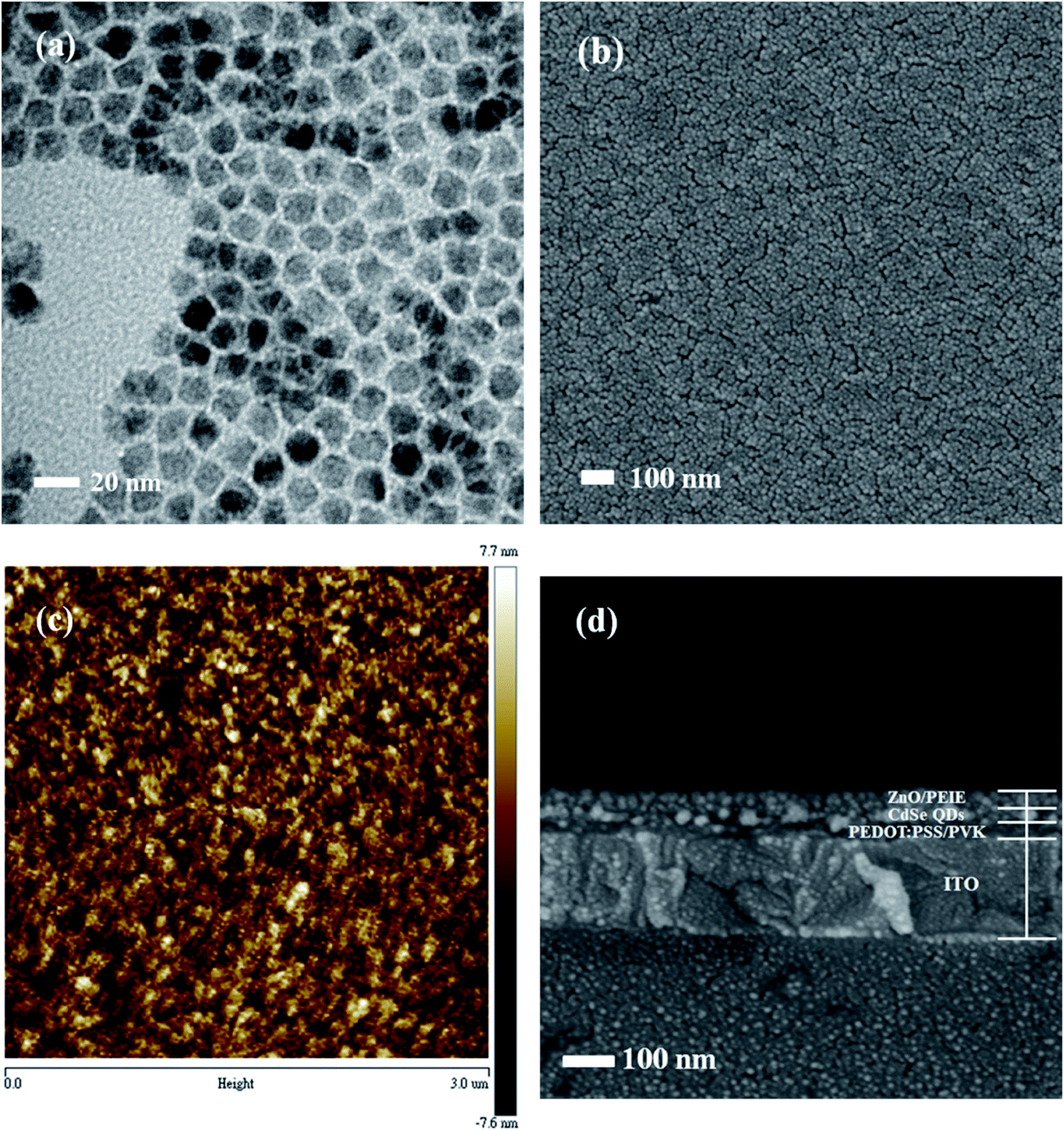 | ||
| Fig. 2 (a) TEM, (b) SEM and (c) AFM images of CdSe QDs; (d) cross-sectional SEM image of the whole device. | ||
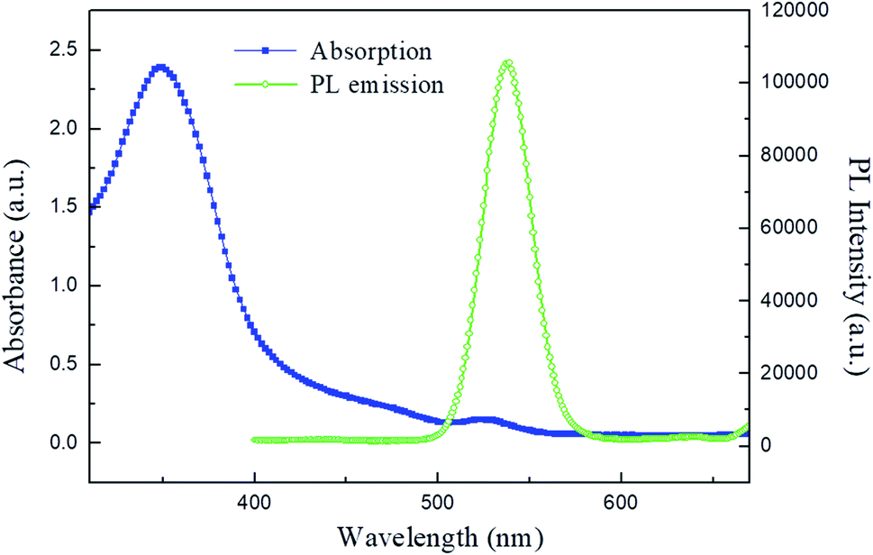 | ||
| Fig. 3 UV-vis absorption and PL emission spectra of CdSe QDs. | ||
To exploit a new device structure for CdSe QDs, four different QLEDs were fabricated for comparison, and the corresponding current density–voltage, brightness–voltage, current efficiency–current density and EQE–voltage characteristics are shown in Fig. 4(a)–(d). The structure of the standard device I is ITO/PEDOT:PSS/PVK/CdSe QDs/ZnO NPs/LiF/Al. The maximum brightness, current efficiency and EQE were measured to be 58985 cd m−2, 9.22 cd A−1 and 2.08%, respectively. For device II, a thin layer of PEIE was deposited on the ZnO NPs for the first time in the development of regular-type QLEDs. We found that the performance of device II with PEIE was dramatically increased, reaching 98563 cd m−2, 26.9 cd A−1 and 6.09%, which are much higher than those of device I. The reason for this phenomenon can be attributed to the lowered CB of ZnO NPs by PEIE and enhanced electron injection from the LiF/Al electrode. In order to further improve device brightness and current efficiency, an additive BYK-P105 from the commercial source was blended with either PVK or PEDOT:PSS to improve the device performance. The structure of device III is ITO/PEDOT:PSS/PVK + BYK-P105/CdSe QDs/ZnO NPs/PEIE/LiF/Al, while the structure of device IV is ITO/PEDOT:PSS + BYK-P105/PVK/CdSe QDs/ZnO NPs/PEIE/LiF/Al. By blending BYK-P105 with PVK, the maximum luminance, current efficiency and EQE of device III were measured to be 39737 cd m−2, 19.6 cd A−1 and 4.44%, respectively, which were significantly reduced compared with device II. By blending BYK-P105 with PEDOT:PSS, the maximum luminance and current efficiency of device IV were surprisingly increased up to 139909 cd m−2, 27.2 cd A−1 and 6.14%, respectively, and the turn-on voltage was notably decreased to 3.8 V. It is seen that the addition of 1 wt% BYK-P105 into different HTLs brought large difference in device performance. Besides, we also prepared 0.5 wt% BYK-P105 in PEDOT:PSS solution to examine its concentration effect. The device performance from 0.5 wt% BYK-P105 has been provided in Fig. S2 and Table S2 in the ESI.† It is seen that the brightness and current efficiency of the QLED were lower than those of the one using 1 wt% BYK-P105. By increasing the concentration to 2 wt%, however, BYK-P105 was not totally dissolved in PEDOT:PSS as observed with the naked eye. We observed that PEDOT:PSS blended with 1 wt% BYK-P105 and showed good film-forming properties since both of them possess an ionic structure. On the contrary, the structural nature of PVK is quite different from that of the additive BYK-P105 that affects miscibility in the solution state. The formed composite film was not very uniform and thus carrier transport ability was prohibited. The top-view SEM images of the two HTLs before and after blending with BYK-P105 are provided in Fig. S3 in the ESI.† It is seen that PEDOT:PSS retained a good film state before and after blending with BYK-P105; however, the PVK film blended with BYK-P105 showed some pinholes and hence the surface of the substrate was not fully covered. The electroluminescence (EL) spectrum of device IV is shown in Fig. 4(e), revealing very bright green light with a maximum EL wavelength at 532 nm. All device performance from the four different QLEDs is summarized in Table 1. The comparison of the device performance of green QLEDs from the previous literature studies and our study is listed in Table 2.4–6,10,20,24,25,27,29,30 It is seen that our optimized device IV comprising PEDOT:PSS + BYK-P105 as the HTL and PEIE-modified ZnO as the ETL showed a very high brightness and comparable current efficiency compared with other studies. Therefore, blending BYK-P105 with PEDOT:PSS provides a successful approach to improve the performance of QLEDs.
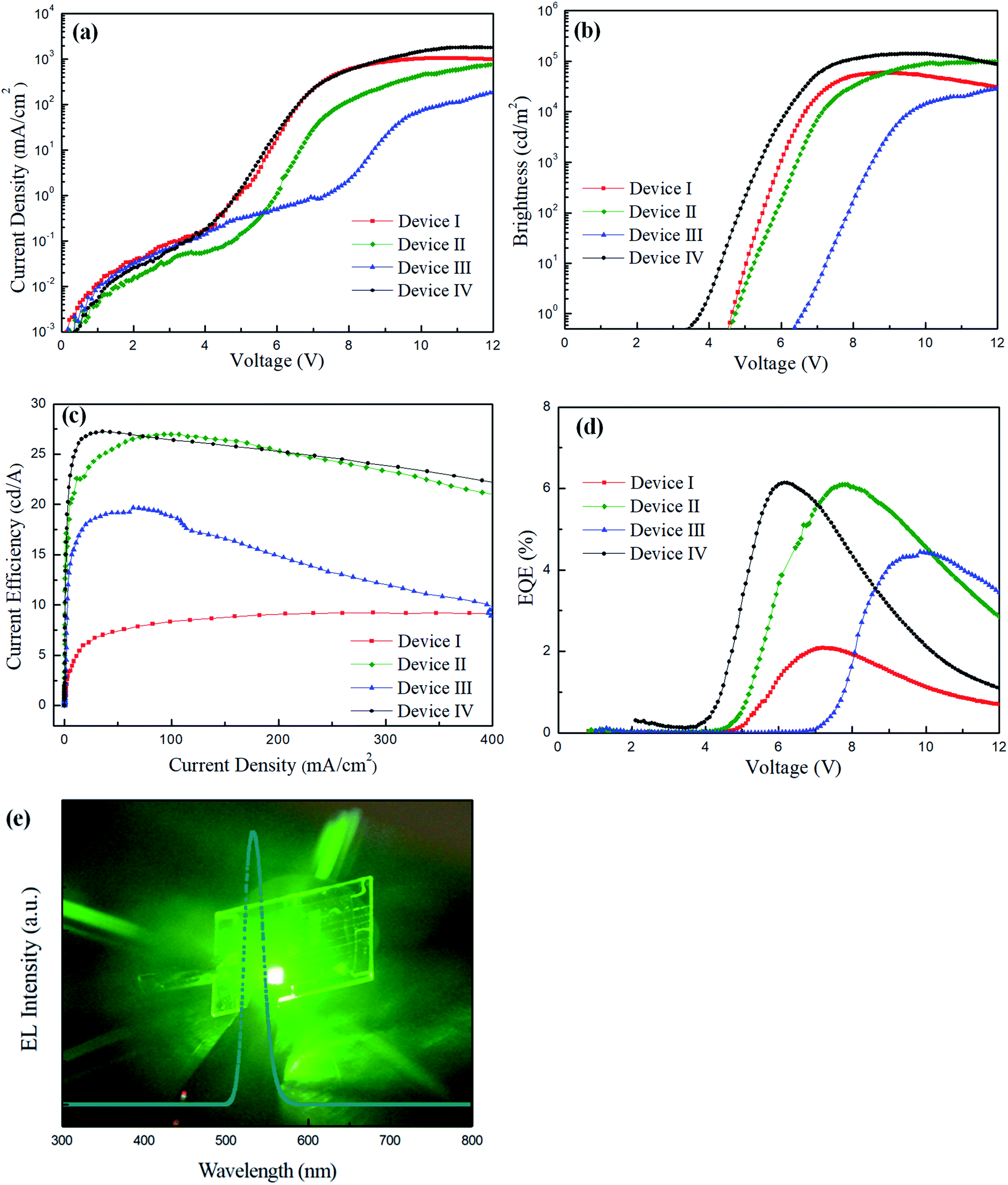 | ||
| Fig. 4 (a) Current density–voltage, (b) brightness–voltage, (c) current efficiency–current density and (d) EQE–voltage characteristics of the four QLEDs; (e) EL spectrum and snapshot of driving device IV. | ||
| Device | Turn-on voltagea (V) | Max brightness [cd m−2 @V] | Max current efficiency [cd A−1 @V] | Max EQE [% @V] |
|---|---|---|---|---|
| a Defined as the operating voltage when the brightness reached 1 cd m−2. | ||||
| I | 4.6 | 58985 @8.85 |
9.22 @7.2 | 2.08 @7.2 |
| II | 4.7 | 98563 @11.5 |
26.9 @7.8 | 6.09 @7.8 |
| III | 6.6 | 39737 @13.8 |
19.6 @9.8 | 4.44 @9.8 |
| IV | 3.8 | 139909 @9.8 |
27.2 @6.15 | 6.14 @6.15 |
| Device structure | V th (V) | L max (cd m−2) | η max (cd A−1) | Ref. |
|---|---|---|---|---|
| ITO/PEDOT:PSS + BYK-P105/PVK/CdSe QDs/ZnO NPs/PEIE/LiF/Al | 3.8 | 139909 |
27.2 | This work |
| ITO/ZnO NPs/CdSe QDs/CBP/MoO3/Al | 2.4 | 218800 |
19.2 | 4 |
| ITO/PEDOT:PSS/Poly-TPD/CdSe QDs/ZnO NPs/Al | 1.8 | 68000 |
7.5 | 5 |
| ITO/WO3 NPs/Poly-TPD/CdSe QDs/ZnO NPs/Al | 3.0 | 21300 |
4.4 | 6 |
| ITO/PEDOT:PSS/TFB/CdSe QDs/ZnMgO/Al | N/A | 52526 |
N/A | 10 |
| ITO/PEDOT:PSS/TFB/core–shell CdSe–ZnSe QDs/ZnO NPs/Al | N/A | 614000 |
N/A | 20 |
| ITO/ZnO NPs/PEIE/core–shell CdSe–ZnS QDs/PVK/PEDOT:PSS/Al | 4.0 | 35860 |
59.1 | 24 |
| ITO/ZnO NPs/PEIE/core–shell CdSe–ZnS QDs/PVK/PEDOT:PSS/Al | 3.8 | 46430 |
91.24 | 25 |
| ITO/PEDOT:PSS/Poly-TPD/Br-capped CdSe QDs/ZnO NPs/Al | 3.0 | 71000 |
6.4 | 27 |
| ITO/PEDOT:PSS/Poly-TPD/CdZnSeS QDs/TPBi/LiF/Al | 3.5 | <16000 |
6.0 | 29 |
| ITO/ZnO NPs/core–shell CdSe–ZnS QDs/PEIE/Poly-TPD/tungsten phosphate/Al | 5.0 | 74160 |
82.2 | 30 |
In order to confirm the enhanced hole transport capability of PEDOT:PSS by adding BYK-P105 and to verify whether charge balance is achieved, two hole-only ITO/PEDOT:PSS/Al and ITO/PEDOT:PSS + BYK-P105/Al devices and one electron-only ITO/ZnO NPs/PEIE/LiF/Al device were fabricated to measure their current–voltage characteristics, as shown in Fig. 5. The device based on PEDOT:PSS + BYK-P105 showed a higher current value, implying better hole transport than the pristine PEDOT:PSS one. The hole mobility of the PEDOT:PSS before and after blending with BYK-P105 was obtained from the space-charge limited current model J = (9/8)εrε0μeV2/d3, assuming εr = 4,10,17ε0 = 8.854 × 10⁻¹² F m−1, and film thickness d = 45 nm. The hole mobility of PEDOT:PSS and PEDOT:PSS + BYK-P105 films was estimated to be 1.13 × 10⁻⁴ and 2.686 × 10⁻⁴ cm2 V−1 s−1, respectively, revealing an enhanced value by using BYK-P105. Moreover, the conductivity of the PEDOT:PSS + BYK-P105 device was closer to that of the ZnO NPs/PEIE device, indicating more balanced carrier transport that is responsible for the improved device performance, as shown in Fig. 4 and Table 1.
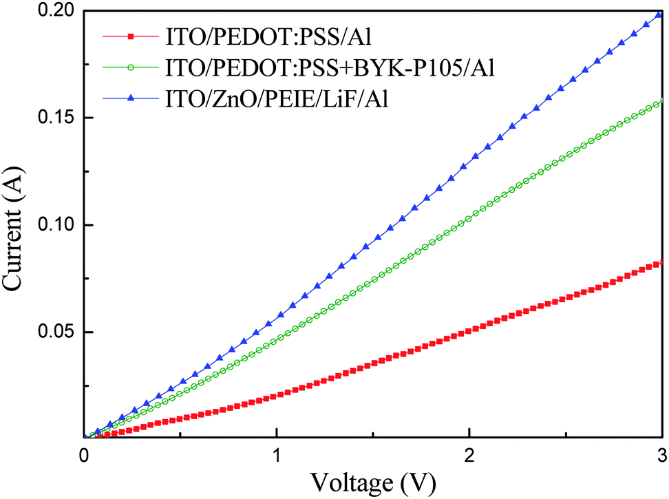 | ||
| Fig. 5 Current–voltage characteristics of the hole-only and electron-only devices. | ||
4. Conclusions
In this research, we successfully fabricated high-efficiency QLEDs by blending BYK-P105 with PEDOT:PSS to modify the hole transport. Meanwhile, for the first time, PEIE-modified ZnO NPs were utilized as the ETL to achieve carrier balance in regular-type QLEDs. The best device exhibited a maximum brightness of 139909 cd m−2 and current efficiency of 27.2 cd A−1 and shows promising use in light-emitting applications.
Conflicts of interest
The authors declare that there is no conflict of interest.Acknowledgements
The authors thank the Ministry of Science and Technology of Republic of China (grant number MoST 107-2221-E-009-042-MY3) for financial support of this work.References
- P. O. Anikeeva, J. E. Halpert, M. G. Bawendi and V. Bulovic, Nano Lett., 2009, 9, 2532–2536 CrossRef CAS PubMed.
- S. Coe, W. K. Woo, M. Bawendi and V. Bulovic, Nature, 2002, 420, 800–803 CrossRef CAS PubMed.
- Y. Yang, Y. Zheng, W. Cao, A. Titov, J. Hyvonen, J. R. Manders, J. Xue, P. H. Holloway and L. Qian, Nat. Photonics, 2015, 9, 259–266 CrossRef CAS.
- J. Kwak, W. K. Bae, D. Lee, I. Park, J. Lim, M. Park, H. Cho, H. Woo, D. Y. Yoon, K. Char, S. Lee and C. Lee, Nano Lett., 2012, 12, 2362–2366 CrossRef CAS PubMed.
- L. Qian, Y. Zheng, J. g Xue and P. H. Holloway, Nat. Photonics, 2011, 5, 543–548 CrossRef CAS.
- X. Yang, Y. Ma, E. Mutlugun, Y. Zhao, K. S. Leck, S. T. Tan, H. V. Demir, Q. Zhang, H. Du and X. W. Sun, ACS Appl. Mater. Interfaces, 2014, 6, 495–499 CrossRef CAS PubMed.
- K. S. Cho, E. K. Lee, W. J. Joo, E. Jang, T. H. Kim, S. J. Lee, S. J. Kwon, J. Y. Han, B. K. Kim, B. L. Choi and J. M. Kim, Nat. Photonics, 2009, 3, 341–345 CrossRef CAS.
- J. Pan, J. Chen, Q. Huang, Q. Khan, X. Liu, Z. Tao, Z. Zhang, W. Lei and A. Nathan, ACS Photonics, 2016, 3, 215–222 CrossRef CAS.
- B. S. Mashford, T. L. Nguyen, G. J. Wilsonb and P. Mulvaney, J. Mater. Chem., 2010, 20, 167–172 RSC.
- S. Wang, Y. Guo, D. Feng, L. Chen, Y. Fang, H. Shen and Z. Du, J. Mater. Chem. C, 2017, 5, 4724–4730 RSC.
- M. N. Kamalasanan and S. Chandra, Thin Solid Films, 1996, 288, 112–115 CrossRef CAS.
- E. Redel, P. Mirtchev, C. Huai, S. Petrov and G. A. Ozin, ACS Nano, 2011, 5, 2861–2869 CrossRef CAS PubMed.
- A. K. K. Kyaw, X. W. Sun, C. Y. Jiang, G. Q. Lo, D. W. Zhao and D. L. Kwong, Appl. Phys. Lett., 2008, 93, 221107 CrossRef.
- D. Zheng, G. Wang, W. Huang, B. Wang, W. Ke, J. L. Logsdon, H. Wang, Z. Wang, W. Zhu, J. Yu, M. R. Wasielewski, M. G. Kanatzidis, T. J. Marks and A. Facchetti, Adv. Funct. Mater., 2019, 29, 1900265 CrossRef.
- E. A. Meulenkamp, J. Phys. Chem. B, 1998, 102, 5566–5572 CrossRef CAS.
- Q. Zhang, X. Gu, Q. Zhang, J. Jiang, X. Jin, F. Li, Z. Chen, F. Zhao and Q. Li, Opt. Mater. Express, 2018, 8, 909–918 CrossRef CAS.
- X. Dai, Z. Zhang, Y. Jin, Y. Niu, H. Cao, X. Liang, L. Chen, J. Wang and X. Peng, Nature, 2014, 515, 96–99 CrossRef CAS PubMed.
- X. Jin, C. Chang, W. Zhao, S. Huang, X. Gu, Q. Zhang, F. Li, Y. Zhang and Q. Li, ACS Appl. Mater. Interfaces, 2018, 10, 15803–15811 CrossRef CAS PubMed.
- D. Li, J. Bai, T. Zhang, C. Chang, X. Jin, Z. Huang, B. Xu and Q. Li, Chem. Commun., 2019, 55, 3501–3504 RSC.
- H. Shen, Q. Gao, Y. Zhang, Y. Lin, Q. Lin, Z. Li, L. Chen, Z. Zeng, X. Li, Y. Jia, S. Wang, Z. Du, L. S. Li and Z. Zhang, Nat. Photonics, 2019, 13, 192–197 CrossRef CAS.
- J. Song, O. Wang, H. Shen, Q. Lin, Z. Li, L. Wang, X. Zhang and L. S. Li, Adv. Funct. Mater., 2019, 29, 1808377 CrossRef.
- H. H. Kim, S. Park, Y. Yi, D. I. Son, C. Park, D. K. Hwang and W. K. Choi, Sci. Rep., 2015, 5, 8968 CrossRef CAS PubMed.
- Y. L. Shi, F. Liang, Y. Hu, M. P. Zhuo, X. D. Wang and L. S. Liao, Nanoscale, 2017, 9, 14792–14797 RSC.
- P. Shen, X. Li, F. Cao, X. Ding and X. Yang, J. Mater. Chem. C, 2018, 6, 9642–9648 RSC.
- F. Cao, D. Zhao, P. Shen, J. Wu, H. Wang, Q. Wu, F. Wang and X. Yang, Adv. Opt. Mater., 2018, 6, 1800652 CrossRef.
- J. Pan, J. Chen, Q. Huang, Q. Khan, X. Liu, Z. Tao, W. Lei, F. Xua and Z. Zhang, RSC Adv., 2015, 5, 82192–82198 RSC.
- B. H. Kang, J. S. Lee, S. W. Lee, S. W. Kim, J. W. Lee, S. A. Gopalan, J. S. Park, D. H. Kwon, J. H. Bae, H. R. Kim and S. W. Kang, Sci. Rep., 2016, 6, 34659 CrossRef CAS PubMed.
- W. K. Bae, J. Kwak, J. W. Park, K. Char, C. Lee and S. Lee, Adv. Mater., 2009, 21, 1690–1694 CrossRef CAS.
- W. K. Bae, K. Char, H. Hur and S. Lee, Chem. Mater., 2008, 20, 531–539 CrossRef CAS.
- F. Cao, Q. Wu and X. Yang, ACS Appl. Mater. Interfaces, 2019, 11, 40267–40273 CrossRef CAS PubMed.
Footnote |
| † Electronic supplementary information (ESI) available. See DOI: 10.1039/c9na00618d |
| This journal is © The Royal Society of Chemistry 2020 |