
 Open Access Article
 This Open Access Article is licensed under a Creative Commons Attribution-Non Commercial 3.0 Unported Licence
The effect of ZnO/ZnSe core/shell nanorod arrays photoelectrodes on PbS quantum dot sensitized solar cell performance
M.
Kamruzzaman

Department of Physics, Begum Rokeya University, Rangpur, Rangpur-5400, Bangladesh. E-mail: kzaman.phy11@gmail.com; Tel: +880-1771034439
First published on 14th November 2019
Abstract
ZnO nanorod (NR) based inorganic quantum dot sensitized solar cells have gained tremendous attention for use in next generation solar cells. ZnO/ZnSe-core/shell NR arrays (NRAs) with various densities were grown on an Au@ZnO seed layer (Au = 0.0, 4.0, 8.0 and 16.0 nm) on glass supported fluorine-doped tin oxide (FTO) substrates using low cost hydrothermal and ion-exchange approaches. PbS quantum dots (QDs) were loaded into the ZnO/ZnSe core/shell NRAs via a successive ionic layer adsorption and reaction (SILAR) method. The morphology, structural and optical properties of the core/shell NRAs were investigated using field emission scanning electron microscopy (FE-SEM), transmission electron microscopy (TEM), X-ray diffraction (XRD) and UV-vis spectroscopy measurements. It was observed that the density of the ZnO/ZnSe NRAs decreases with increasing Au buffer layer thickness. The absorption decreases along with a decrease in the ZnO/ZnSe NRA density. The ZnO NRs/PbS QD photoelectrode performs poorly; however, after introducing a ZnSe shell on the core-ZnO, the solar cells parameters changed according to the ZnO/ZnSe NRA density. Values of η = ∼0.88%, JSC = 14.60 mA cm−2, and VOC = 190 mV, and η = ∼0.25%, JSC = 6.77 mA cm−2, and VOC = 115 mV were obtained for the highest and lowest NRA densities, respectively. Although the photovoltaic performance of these photoelectrodes is still inferior, further improvement of the device would be possible by suppressing surface defects, and through quality optimization of the ZnO/ZnSe NRAs, PbS QDs, counter electrode and electrolyte.
1. Introduction
Quantum dot (QD) sensitized nanostructure based solar cells have been attracting a tremendous amount of attention in the development of an alternative to silicon-based solar cells.1 Inorganic quantum dot solar cells (QDSSCs) are promising for next generation solar cells due to their low-cost cell fabrication and high power conversion efficiency.2–12 This type of photovoltaic cell is a modification of the dye synthesized solar cell (DSSC),13,14 which was first introduced by O'Regan and Grätzel in 1991.14 The efficiencies of QDSSCs are lower than those of DSCs,15 which implies that some challenges still remain in enhancing the performance of QDSSCs. The power conversion efficiency (PCE) of these solar cells has risen to over 11.6%.16–23 QDSSCs are more attractive than DSSCs due to the fact that QDs are promising efficient light harvesting candidate materials for sensitized solar cells.24 QDs have been used as a sensitizer due to them having several excellent properties such as; that their band gap can be tuned via a size dependent quantum confinement effect,25 they have higher absorption coefficients,26 multiple exciton generation (MEG),27 the possibility of hot electron injection,28 extended photostability, impact ionization effects and simple fabrication processes.29 Various narrow band gap inorganic semiconductors QDs such as CdS,30 CdSe,31 CdHgTe,32 InAs,32 CISeS,33 Zn–Cu–In–Se,16 CdTe,34 and PbS35 have been used as sensitizers. C. Y. Luan et al. and Lee et al. reported efficiencies of 0.27% and 0.59% for CdS QD-sensitized ZnO NR-based solar cells.30,36 The efficiency of CdSe QD-sensitized ZnO nanotube array based solar cells is around 0.44%.31 TiO2 nanostructured solar cells decorated with CdHgTe QDs and InAs QDs exhibit PCEs of around 0.81%31 and 0.3%,32 respectively. CuInSexS2−x and Zn–Cu–In–Se QD sensitized solar cells have efficiencies of around 5%33 and 11.61%.16 The efficiencies of core/shell CdSe/CdTe and CdTe/CdSe structures have been reported to be around 0.14% and ∼0.38%.34 The PCE of a PbS QD sensitized TiO2 nanoparticle thin film solar cell was found to be 3.88%.34 Baxter and Aydil have reported an efficiency of 0.5% for a ZnO NW-based solar cell.37 A vertical oriented ZnO NR based hybrid-polymer/ZnO photovoltaic device demonstrated an efficiency of 0.2%.38 An efficiency of 0.22% has been reported for a ZnO NR-based dye-synthesized solar cell.39 Recently, wide band gap metal oxides QDs have also been used to improve charge transfer properties and reduce the charge recombination rate.16 In addition, QD sensitized solar cell devices can be printed in a roll-to-roll manner using compatible techniques. Among the various QDs, lead sulfide (PbS) QDs have been chosen as a sensitizer for the development of photo-energy conversion efficiency25–35,40 and photodetector performance32 because of their unique properties such as size-dependent tunable band gap in between 0.41 (bulk) and 4.0 eV34,40, multiple exciton generation (MEG),41 high absorption coefficient and good photostability. PbS QDs exhibit strong quantum size effects compared to CdS and CdSe QDs29 for a QD size of <18 nm.To construct QD-sensitized solar cells, a general strategy is essential to design and select new materials as well as novel nanostructures for electron transporting and QD loading. In this case surface morphologies play a crucial role in improving electron mobility associated with ordered metal oxide nanostructures. The nanostructures of SnO2, TiO2, WO3 and ZnO metal oxides have been studied for several years. Among these oxides, the nanostructures of TiO2 and ZnO have been extensity and intensively investigated.42–48 Although TiO2 possesses an almost similar band gap and physical properties as those of ZnO, ZnO is the most suitable semiconductor material for photoanode applications.44–48 One dimensional (1D) ZnO NRs/NWs exhibit much higher electron mobility (155 cm2 V−1 s−1vs. 10−5 cm2 V−1 s−1) and large exciton diffusion lengths,49 low sensitivity to UV degradation and long term stability, which means that ZnO is a good alternative material to TiO2.43 Importantly, the nanostructures and morphology of ZnO can be simply controlled.50 A 1D ZnO-NR/NW nanostructure provides a direct pathway for the carrier transportation of photoinduced electrons if it is used as a photoanode, which might suppress charge recombination51–53 and hence the efficiency can be improved via the utilization of controllable nanostructured arrays. Furthermore, the infiltration of tunable size QDs in nanostructures can effectively improve the photovoltaic PCE.50,54–58 However, the performance of QDSSCs not only depends on the photoanode and QDs, but also on the counter electrode (CE) as well as on the electrolyte. The CE is an important issue in the development of efficient QDSSCs. Electrolyte improvement is needed to overcome the poor charge transfer of the CE to the oxidized redox electrolyte species, which greatly affects the fill factor and PCE.
In this report, ZnO/ZnSe core/shell NR arrays with various densities have been grown via hydrothermal and ion exchange approaches for QDSSC applications. The PbS QDs are loaded in the pores and/or on the walls of the vertically oriented ZnO/ZnSe core/shell NR arrays to increase the mobility of the carriers.58,59 Cu2S is used as a CE due to its superior performance in QDSSCs, in terms of its low cost, facile fabrication, high electrocatalytic activity and good stability. On the other hand, an electrolyte that operates via a polysulfide redox couple (Sn2−/S2−) is used for testing device performance owing to the effective stabilization of QDs and to improve the performance of QDSSCs.57,60
The purpose of this work is to investigate the effect of the physical properties of various densities of 1D ZnO/ZnSe core/shell NRAs on photoelectrode performance. Firstly, ZnO (core) NR arrays were synthesized on a modified Au@ZnO seed layer (Au = 0.0, 4.0, 8.0 and 16.0 nm) via a hydrothermal approach and then ZnO (core) was coated with a ZnSe shell via an ion exchange approach consisting of ZnO/ZnSe (core/shell) NRAs. The ZnSe shell is used to enhance the optical absorption attributed to reducing the band gap and enhancing the surface area for accommodating more QDs. As a sensitizer, PbS QDs infiltrate into the NRAs to enhance the light harvesting properties of the ZnO/ZnSe photoelectrode. A detailed synthesis process, characterization, and photoelectric performance of the photoelectrodes are discussed.
2. Experimental
The substrate cleaning, ZnO seed layer preparation and ZnO NR arrays growth have been described in previous papers.8,9,58,61 Briefly, a seed layer was prepared on cleaned glass supported fluorine-doped tin oxide (FTO) substrates via a spin coating method. A sol gel solution of zinc acetate dehydrate (0.03 M) and ethanolamine (0.03 M) was spin coated on the substrates at 2500 rpm for 1 min and the film was dried at a temperature of 200 °C. The process was repeated twice followed by thermal annealing at 400 °C for 30 min. Buffer layers of Au (0.0, 4.0, 8.0, and 16.0) nm were deposited on the ZnO seed layer via a thermal evaporation method under a pressure of 2.2 × 10⁻⁶ Torr. The modified Au@ZnO seed layers were then annealed at 350 °C for 30 min. After that, the modified seed layer substrates were suspended face down in an equimolar concentration (0.025 M) of an aqueous solution of zinc nitrate hexahydrate and hexamethylenetetramine (HMTA) at a temperature of 90 °C for 5 h. The process was repeated six times to grow the desired NR arrays. The final ZnO NR array products were annealed in the air at 350 °C for 30 minutes to remove inorganic salts or impurities and to improve crystallinity. Then, the ZnO/ZnSe core/shell NR arrays were synthesized by immersing ZnO NR arrays in a mixture of an aqueous solution of Se powder and NaBH4 (8 mm) at 55 °C for 3 h. The process was repeated for a second time to obtain a ZnSe shell with the desired thickness. After that, PbS QDs were loaded onto the ZnO/ZnSe NR core/shell NR arrays via a successive ionic layer adsorption and reaction (SILAR) method. Firstly, a ZnO/ZnSe NR core/shell was dipped into a 0.1 M lead nitrate Pb(NO3) aqueous solution for 1 min to form Pb2+ ions and then a further 1 min into a 0.1 M sodium sulfide (Na2S) aqueous solution to allow S2− to react with the pre-adsorbed Pb2+, leading to the formation of PbS QDs. The procedure was repeated 5 times and the substrate was rinsed with deionized (DI) water between the dips.To produce the final ZnO NR, ZnO/ZnSe core/shell NR array and PbS QD, the following chemical reactions eqn (1)–(3) were took place:58,62–64
| Zn(NO3)·6H2O + (CH2)6N4 ↔ ZnO + H2O | (1) |
| Se + 2NaBH4− + H2O ↔ ZnSe + 2OH− + H2 + 2BNaH3 | (2) |
| Pb(NO3)2 + Na2S·9H2O + H2O ↔ PbS + 2NaOH + H2 + 7H2O | (3) |
2.1 Electrolyte
To investigate the performance of the ZnO/ZnSe/PbS QD photoelectrode, a polysulfide electrolyte was made from aqueous solutions of 1.0 M S, 0.1 M NaOH, and 1.0 M Na2S, which is a good noncorrosive redox couple for QD solar cell devices.58 It is used to develop the performance of QDSSCs by reducing the charge recombination between the electrolyte and counter electrode. A low-volatile solvent (DI water) was used to increase the durability of the solar cells.582.2 Counter electrode
A Cu2S counter electrode was prepared by immersing a brass sheet in a HCl solution (37 wt%) at a temperature of 70 °C for 7 min and subsequently dipping it into a polysulfide aqueous solution of 1.0 M S, 0.1 M NaOH, and 1.0 M Na2S for 5 min. It is used as an electron collector to circulate through the external circuit and improve the device performance.582.3 Device fabrication
The solar cells were prepared using two electrodes, (ZnO/ZnSe NRs/PbS QDs and the counter electrode) separated by a 60 μm thick polypropylene spacer, and the internal space of the cells was filled with a polysulfide electrolyte. The active area of each photoelectrode was 0.05 cm2 and the device structure is shown in Fig. 6(a).582.4 Characterization
The nature of the surface of the materials was investigated by field emission scanning electron microscopy (FE-SEM, Philips). The crystallinity and crystal structures of the samples were investigated using X-ray diffraction (XRD, Rigaku Smart) and transmission electron microscopy (TEM, Philips). SEM images were collected using an acceleration voltage of 20 keV, spot size of 3 and working distance of ∼10 mm. TEM images were collected using a high resolution TEM at 200 keV. XRD data were taken in the range of 20° to 70° with a step width of 0.02°. UV-vis spectra were collected at RT in the wavelength range of 350 to 1100 nm (PerkinElmer Lambda). The current density (J)–voltage (V) readings were measured with the assistance of air mass 1.5 global (AM1.5G) illuminations apparatus, a calibrated solar simulator with an intensity of 100 mW cm−2 (1-sun).3. Results and discussion
3.1 X-ray diffraction
Fig. 1A(a)–(d) shows the XRD patterns of the (a) FTO substrate, (b) ZnO NRs, (c) ZnO/ZnSe core/shell and (d) ZnO/ZnSe NRs/PbS QDs. In this case, the ZnO NRs, ZnO/ZnSe and ZnO/ZnSe/PbS were grown on an Au free ZnO seed layer, i.e., Au = 0.0 nm. It can be seen that a few diffraction peaks come from the FTO substrate (Fig. 1A(a)). In Fig. 1A(b), several extra peaks can be observed around the diffraction angles 2θ = ∼31.80°, ∼34.42°, ∼36.28°, ∼47.56°, ∼56.66°, ∼62.66° and ∼66.46°. These peaks can be properly indexed as belonging to the (100), (002), (101), (102), (110), (103) and (200) planes, corresponding to hexagonal structured ZnO NRs (JCPDS card no. 036-1451). It is obvious that the intensity of the (002) peak is greater than that of the other peaks, attributed to the preferential vertical orientation along the (002) plane and [0001] direction, normal to the substrate surface. The preferential orientation of ZnO along the (002) plane can be attributed to the minimum surface free energy, minimum internal stress and high atomic density, which lead to the easy growth of the crystal.65 Importantly, some additional peaks in the ZnO/ZnSe (Fig. 1A(c)) spectrum associated with ZnO NRs (Fig. 1A(b)) at 2θ = ∼27.65°, ∼45.13° and ∼52.67° correspond to the index planes (111), (220) and (311) for cubic zinc blend structured ZnSe (JCPDS card no. 65-9602).68 The appearance of these peaks in the XRD pattern is good evidence for ZnO/ZnSe NR (core/shell) crystal formation and is in good agreement with the TEM image (Fig. 4). Besides these peaks, three additional peaks are observed in the diffraction pattern of ZnO/ZnSe/PbS QDs (Fig. 1A(d)) at 2θ = ∼23.55°, ∼29.58° and ∼43.83°, corresponding to the Miller indices (111), (200) and (220), attributed to the cubic phase of PbS (JCPDS no. 41-1049). Thus, the appearance of these peaks in the XRD patterns suggests that the structure consists of a ZnO/ZnSe/PbS QD photoelectrode.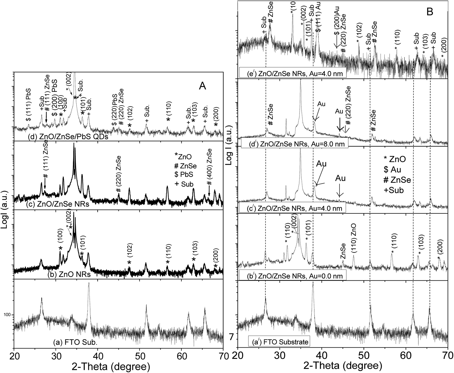 | ||
| Fig. 1 (A) XRD patterns of the (a) FTO sub., (b) ZnO NRs, (c) ZnO/ZnSe NRs and (d) ZnO/ZnSe/PbS QDs. (B) XRD patterns of the (a/) FTO sub., (b/) ZnO/ZnSe NRs, Au = 0.0 nm, (c/) ZnO/ZnSe NRs, Au = 4.0 nm, (d/) ZnO/ZnSe NRs, Au = 8.0 nm and (e/) ZnO/ZnSe NRs, Au = 16.0 nm NRAs with various densities. | ||
Fig. 1B shows the XRD patterns of the FTO substrate (Fig. 1B(a/)) and NRAs with various densities of ZnO/ZnSe (Fig. 1B(b/)–(e/)) coupled with an increase in the Au buffer layer thickness (Au = 0.0, 4.0, 8.0 and 16.0 nm). It is interesting that the sharpness of the peaks decreases with increasing buffer layer thickness up to Au = 8.0 nm, and the peak positions shift toward a higher angle (Fig. 1B(b/)–(d/)). However, the peaks positions shift significantly for the Au = 16.0 nm buffer layer (Fig. 1B(e/)) thickness indicating that a thicker Au buffer layer exerts more stress on ZnO/ZnSe NR growth as a result of NRs not being perfectly grown vertically on the substrate, which is in good agreement with the SEM images (Fig. 3(f)). No peak is visible for Au in the diffraction pattern of Fig. 1B(b/), reflecting that the ZnO/ZnSe NRAs have grown on the Au free ZnO seed layer. However, a few peaks can be seen in the diffraction patterns for Au (Fig. 1B(c/)–(e/)) indicating that these ZnO/ZnSe NRAs have grown on the Au = 0.0 nm coated ZnO seed layer. The intensity of the (111) diffraction peak increases with increasing Au buffer layer thickness, which is in good agreement with the SEM images (shown in Fig. 2(b) and (c).) It can be clearly seen that all of the crystallographic planes for the ZnO NRs are still present in all of the diffraction patterns, confirming the existence of wurtzite structured ZnO/ZnSe core/shell NRs.
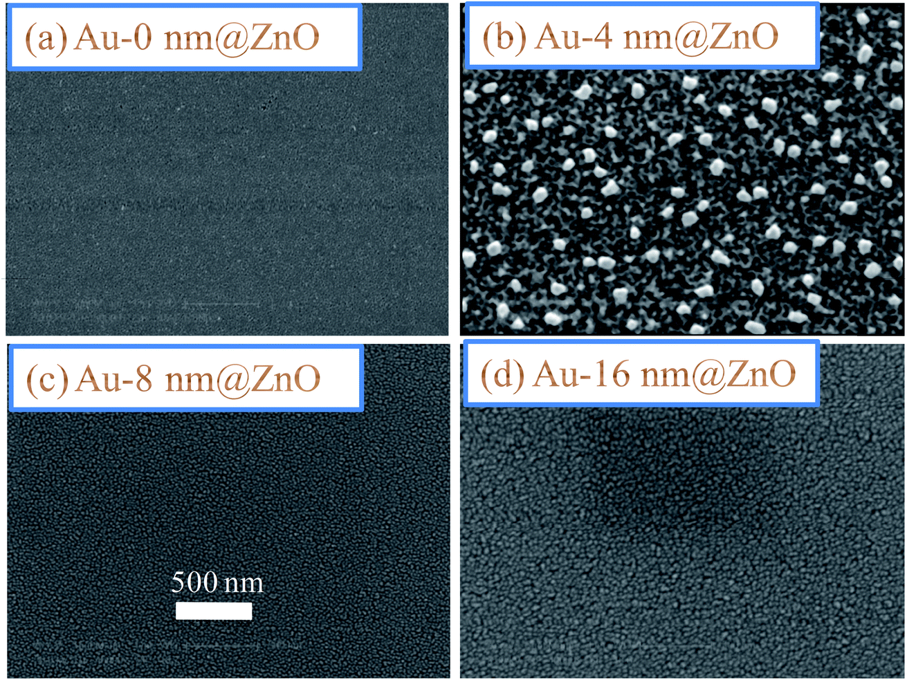 | ||
| Fig. 2 Surface morphologies of ZnO seed layers modified with Au (0.0, 4.0, 8.0 and 16 nm) buffer layers: (a) Au-0 nm@ZnO, (b) Au-4 nm@ZnO, (c) Au-8 nm@ZnO, and (d) Au-16 nm@ZnO seed layers (scale bar 500 nm). | ||
3.2. Surface morphology measurements using SEM
Fig. 2(a)–(d) show the surface morphologies of ZnO seed layers modified by the deposition of Au (0.0, 4.0, 8.0 and 16.0 nm) buffer layers. It can be clearly seen that the Au free ZnO seed layer (Fig. 2(a)) is smoother, uniformly covering the whole substrate surface in a defect free manner with no voids.After depositing the Au buffer layer on the ZnO seed layer (Fig. 2(b)–(d)), the samples were annealed at 350 °C under identical thermal conditions. This led to the formation of nanometer-sized Au grains (clusters), which were dispersed on ZnO seed layer. By comparing the images, it can be seen that there is a large variation in the size distribution of Au grains depending on the thickness of the Au buffer layers. For the Au = 4.0 nm thickness, an overall low density of nanograins/clusters can be observed in the seed surface, attributed to the agglomeration of smaller grains in the thin Au buffer layer.66 As the thickness of the Au increases, the grains of Au become noticeably larger and more compacted (Fig. 2(c) and (d)). Such morphology suggests that the Au buffer layers agglomerate into nanosized grains/clusters which play a pivotal role in the controllable growth of ZnO/ZnSe NRAs as is desirable for nanoelectronic and optoelectronic devices.
Fig. 3 shows the surface morphologies and cross-section views of the ZnO NRs (Fig. 3(a)) grown on the Au free ZnO seed layer and ZnO/ZnSe core/shell NRAs (Fig. 3(b)–(e)) grown on the Au modified ZnO seeded layers. From Fig. 3(b)–(e), it can be seen that the average core/shell ZnO/ZnSe NR array density (μm−2) changes considerably with an increase in the Au buffer layer thickness (Au = 0.0 to 16.0 nm), which is in good agreement with previous reports.67–74 As the ZnO seed layers are coated with the Au buffer layer, the nucleation site of the ZnO seeds possibly decreases, which might inhibit the growth of ZnO/ZnSe NRAs resulting in a decrease in the NR array density.73,74 Although the density of the ZnO/ZnSe NR arrays can be controlled, simultaneous control of nanostructure morphology, density, and aspect ratio (length/diameter) are still challenging issues for a facile hydrothermal method.67,68,70–75 In this study, it can be seen that with an increasing in the Au buffer thickness that both the length and diameter of the ZnO/ZnSe NRs change. The length and diameter of the NRs change in the range of 1.79–2.08 μm and 50–100 nm, respectively, in accordance with increasing Au buffer layer thickness. It is expected that the diameter of the NRs mainly depends on the nature of the ZnO seed layer. However, as the thickness of Au is increased, then the sizes of the granules/clusters of Au increase, compactly covering the ZnO seed layer (Fig. 2(b) and (c)). As a result, the diameter of the NRs grown on a thicker Au buffer layer is increased compared with those grown on an Au free ZnO seed layer. This change can be explained by the decrease in the nucleation agents of the ZnO seed layer for the growth of ZnO/ZnSe NRs.
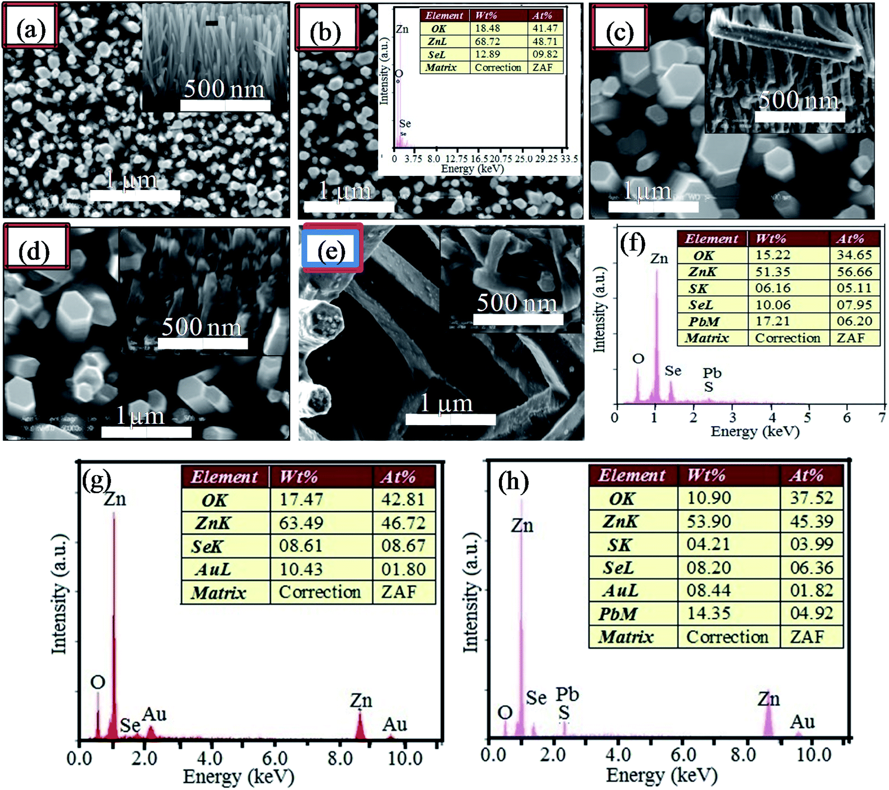 | ||
| Fig. 3 Top and side views (inset) of the ZnO NR arrays grown on the ZnO seed layer (a). Top and side views of the ZnO/ZnSe core/shell NRAs grown on (b) Au@ZnO, Au = 0.0 nm, (c) Au@ZnO, Au = 4.0 nm, (d) Au@ZnO, Au = 8.0 nm, and (e) Au@ZnO, Au = 16.0 nm seed layers (scale bars for the top of 1 μm and side of 500 nm). EDX spectra of the ZnO/ZnSe NRs (inset, (b)) and (f) ZnO/ZnSe/PbS QDs grown on an Au free ZnO seed layer. EDX spectra of (g) ZnO/ZnSe NRs and (h) ZnO/ZnSe/PbS QDs grown on an Au = 8.0 nm coated ZnO seed layer. | ||
Fig. 3(b) (inset) shows the energy dispersive X-ray (EDX) spectrum of ZnO/ZnSe core/shell NRs grown on an Au free ZnO seed layer. Three peaks of Zn, O and Se can be observed, indicating that the grown NR array is ZnO/ZnSe. The EDX spectrum of the ZnO/ZnSe/PbS QD structure grown on the Au free ZnO seed layer is shown in Fig. 3(f). Four elemental peaks for Zn, O, Se, Pb and S are present in the spectrum with proper stoichiometric percentages, confirming that ZnO NRs were uniformly coated with the Se, Pb and S elements. The EDX spectra of the ZnO/ZnSe NR and ZnO/ZnSe/PbS QD structures grown on an Au coated ZnO seed layer are shown in Fig. 3(g) and (h). Importantly, an additional peak for Au can be seen in both spectra with proper stoichiometry, providing evidence that the ZnO/ZnSe NRs and ZnO/ZnSe/PbS QDs have been grown on the Au coated ZnO seed layer.
3.3 Transmission electron microscopy (TEM)
Fig. 4A (left side) shows a low resolution image of intrinsic ZnO NRs (Fig. 4A(a)) and core/shell ZnO/ZnSe (Fig. 4A(b)), selected area electron diffraction (SAED) of ZnO/ZnSe (Fig. 4A(c)) and a high-resolution transmission electron microscopy (HRTEM) image of the ZnO/ZnSe/PbS QDs (Fig. 4A(d)). From Fig. 4A(a), it can be clearly seen that the single ZnO NR possesses a diameter of less than 100 nm. The ZnO/ZnSe consists of a core/shell-like structure, which is indicated by an arrow (Fig. 4A(b)). The SAED image of ZnO/ZnSe exhibits that the grown NR is single crystalline in nature (Fig. 4A(c)). The HRTEM shows a well-defined lattice fringe separation of ∼5.13 nm corresponding to the lattice constant ‘c’, meaning that the NRs have grown along the c-axis. This result indicates that the NRs have a high quality single-crystalline structure with a growth orientation along the [0001] direction, which is in good agreement with the SAED and XRD results. In addition, the d-spacing in between the crystal planes is about ∼2.67 nm, which is good agreement with the XRD results (Fig. 1A and B). Fig. 4B(a/) and (b/) shows TEM images of ZnO and ZnO/ZnSe grown on an Au = 8.0 nm coated ZnO seed layer. The SAED and HRTEM results of the ZnO/ZnSe/PbS QDs are shown in Fig. 4B(c/) and (d/). In Fig. 4B(d/), an area is enclosed by a white dotted line, which shows the average size of the PbS QDs. After analysis of the HRTEM, it can be concluded that a synthesized PbS QD size of ∼5.75 nm with a lattice constant of ∼0.24 nm was adsorbed on the ZnO/ZnSe core/shell NRA photoelectrode.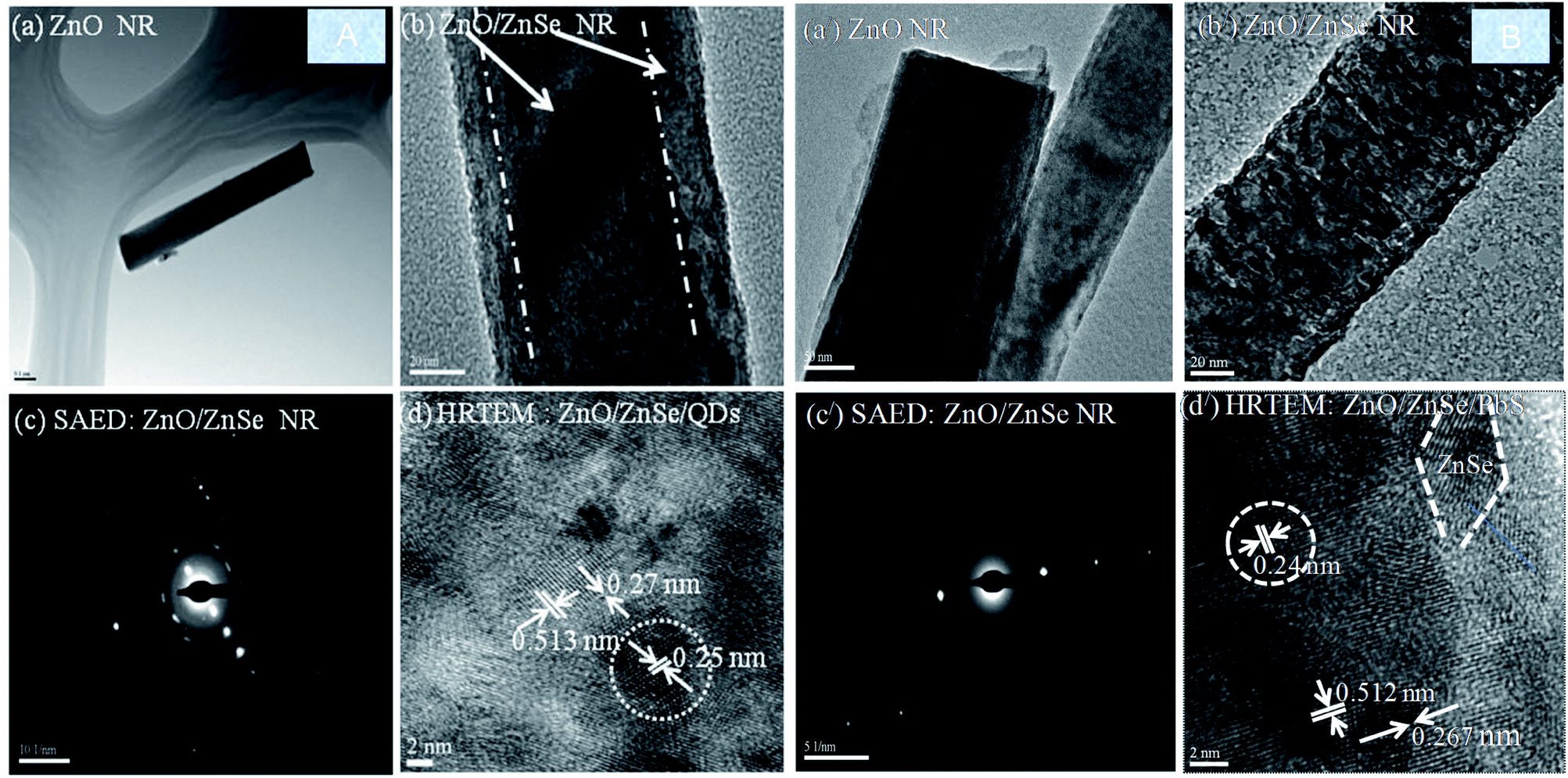 | ||
| Fig. 4 (A) TEM images (left side) of (a) pure ZnO NRs, and (b) core–shell ZnO/ZnSe NRs, (c) SAED pattern of the ZnO/ZnSe NRs and (d) HRTEM image of the ZnO/ZnSe/PbS QDs grown on an Au free ZnO seed layer. (B) TEM images of (a/) pure ZnO NRs, and (b/) core–shell ZnO/ZnSe NRs, (c/) SAED pattern of the ZnO/ZnSe NRs and (d/) HRTEM image of ZnO/ZnSe/PbS QDs grown on an Au = 8.0 nm coated ZnO ZnO seed layer. | ||
Fig. 4B(a/)–(d/) show TEM images of the ZnO/ZnSe and ZnO/ZnSe/PbS structures grown on an Au (Au = 8 nm) coated ZnO seed layer. In this case, it can be seen that the core–shell (ZnO/ZnSe) morphology is rougher (Fig. 4B(b/)) than when grown on the Au free ZnO seed layer (Fig. 4A(b)). The SAED pattern (Fig. 4B(c/)) and HRTEM lattice fringes (Fig. 4B(d/)) show small changes that can be attributed to the coating of Au on the ZnO seed layer. However, the photoelectrode consists of a ZnO/ZnSe/PbS QS structure, which is indicated by different white symbols (QD = white circle area, ZnSe = parallelogram area, ZnO = straight line with lattice constants).
3.4 Optical properties (absorption)
Fig. 5 shows the absorption spectra of the ZnO NRAs, ZnO/ZnSe (core/shell) NRAs and NRA density variation in the ZnO/ZnSe/PbS QDs. The inset digital image shows changes in color associated with the changes in the structures. From Fig. 5 (inset), it can be seen that the ZnO NRAs exhibit (white), ZnO/ZnSe NRs (orange) and ZnO/ZnSe/PbS QDs (black), respectively. The absorption edge of ZnO is located at around 380 nm and exhibits less absorption of light. However, the ZnO/ZnSe core/shell NRAs demonstrate that more light can comparatively be absorbed than for the ZnO NRAs. The absorption edge is shifted toward a higher wavelength, which lowers the band gap of the ZnO/ZnSe NRAs. Therefore, the optical absorption of ZnO can be enhanced by creating a ZnSe shell or more defects (e.g., metal ions doping) on the pure ZnO NRA surfaces. | ||
| Fig. 5 The absorption spectra in the wavelength range of 370–1100 nm of the pure ZnO NRs, and ZnO/ZnSe NRs/PbS QDs with increasing Au (Au = 0.0, 4.0, 8.0 and 16.0 nm) thickness. | ||
In this case, large numbers of hole–electron pairs could be generated even without the presence of UV light.76 Hence, the efficiency of the ZnO/ZnSe NR array based solar cell can be increased. It is interesting that the absorption is significantly enhanced in the visible to near infrared region (630–910 nm) for the ZnO/ZnSe/PbS QD structure, which can be attributed to the PbS QDs. This value gradually decreases with a decrease in the ZnO/ZnSe NRA density, implying that fewer QDs are loaded into lower ZnO/ZnSe NR array density surfaces. The band gap of the PbS QDs was found to be ∼1.75 eV, which is in good agreement with the reported value.58 The enhancement in the optical ability of the ZnO/ZnSe/PbS QD photoelectrode in the visible to near infrared region, making it promising for application in photovoltaic devices.
3.5 J–V characteristics
In an earlier publication, the solar cell performance for a specified NRA density was reported.58Fig. 6(a) shows a prototype ZnO NR-based QDSC for electron–hole pair generation and their transport mechanism in the device. The solar cell consists of ZnO/ZnSe (core/shell) NR arrays, QD sensitizer, polysulfide electrolyte and a counter electrode. In this case, the ZnO/ZbSe NR arrays serve as a backbone for direct electron transport providing short transport distances in the ZnO/ZnSe/PbS QDs solar cell. Under the illumination of light, photons are captured by PbS QDs yielding electron–hole pairs that are rapidly separated into electrons and holes at the interface between the ZnO/ZnSe NRs and PbS QDs. The electrons are quickly injected into the conduction band of ZnSe then into ZnO and the holes are released by redox couples (S2−/Sn2−) in the electrolyte.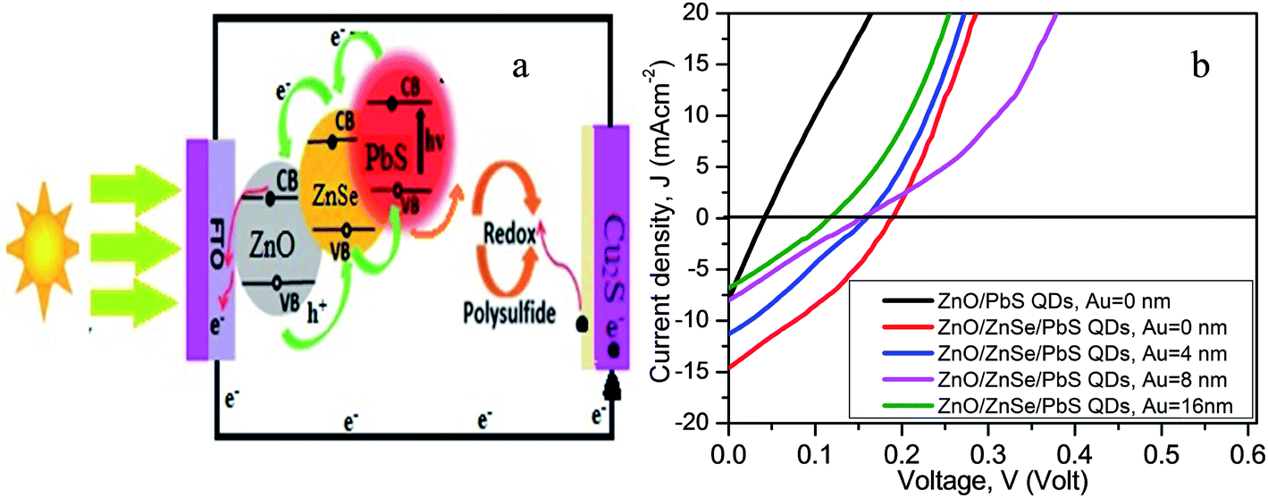 | ||
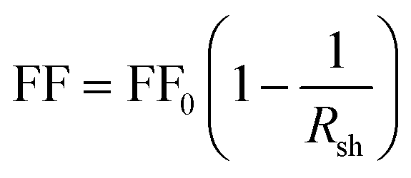
| Fig. 6 (a) Electron–hole transport mechanism [ref. 58], and (b) the J–V characteristics of the glass/FTO/ZnO/PbS QDs (black line) and ZnO/ZnSe NRA density varying glass/FTO/ZnO/ZnSe NRs/PbS QD solar cells. | ||
Fig. 6(b) shows the photocurrent density (J)–voltage (V) characteristics of the ZnO NRs/PbS QDs and NR array density variation of the ZnO/ZnSe/PbS QDs solar cells. The photoelectrode performance parameters such as short-circuit current density (JSC), open-circuit voltage (VOC), fill factor (FF), efficiency (η), series resistance (Rs) and shunt resistance (Rsh) for all of the devices are summarized in Table 1. From Fig. 6(b) (black line) and Table 1, it can be clearly seen that the ZnO NR-based solar cell fabricated as a ZnO/PbS QD device performed poorly with values of η = 0.079%, JSC = 7.92 mA cm−2 and VOC = 0.04 V, which could be due to its inability to capture more photons, resulting in the generation of fewer electron–hole pairs. The obtained results are consistent with the absorption phenomenon of the ZnO NR arrays shown in Fig. 5, in that the cell can absorb fewer photons in the visible region. It is interesting that the performance of the ZnO/ZnSe core/shell NR-based devices (ZnO NRs coated ZnSe) is significantly enhanced compared to that of ZnO NR-based devices (Table 1) and the solar cell parameters change with the variation in the ZnO/ZnSe NRA density (Fig. 6(b)). As the ZnSe (shell) is coated on the ZnO NRs (core), the band gap of ZnO/ZnSe is reduced and the surface defects are suppressed, consequently leading to the more effective absorption of photons.54–58 The PbS QD solar cell assembled using the highest ZnO/ZnSe NRA density exhibits a high performance of η = 0.88%, JSC = 14.60 mA cm−2, VOC = 0.19 V and FF = 0.32. Compared with the ZnO NR photoelectrode, the ZnO/ZnSe NR photoelectrode displays significantly enhanced η, JSC, VOC and FF values, which could be due to an increase in the efficiency of QD loading, suppression of surface defects, reduction in electron loss and decrease in the band gap of ZnO/ZnSe.54–58 The assembled QD device with the highest density of ZnO/ZnSe NRAs not only shows improved charge transport phenomena but also allows for the efficient loading of QDs to provide more active sites for generating large numbers of electron–hole pairs and to catalyze the reduction of Sn2− to nS2, hence enhancing the efficiency of the device.54–56,77 The improved morphology of the ZnO/ZnSe NRs offers efficient transport channels to ensure the rapid transportation of electrons due to band gap lowering, and thus the charge combination process can be suppressed, also leading to an increase in performance.55–58 As the density of the ZnO/ZnSe NRAs decreases, the photovoltaic performance decreases, which can be attributed to a decrease in the surface area for QD loading (shown in Fig. 3(b) and Table 1) and the production of too many defects, resulting in electron loss. The solar cell parameters for the PbS QD device with the lowest ZnO/ZnSe NRA density were obtained as η = 0.25%, JSC = 6.76 mA cm−2, VOC = 0.13 V and FF = 0.28 (Table 1). The lower value of VOC for the lowest ZnO/ZnSe NR array density can be attributed to the existence of large defects.
| Device name | J SC (mA cm−2) | V OC (volt) | FF | η (%) | R s (ohm) | R sh (ohm) |
|---|---|---|---|---|---|---|
| ZnO/PbS QDs, Au = 0 nm | 7.92 | 0.04 | 0.252 | 0.079 | 4.202 | 7.77 |
| ZnO/ZnSe/PbS QDs, Au = 0 nm | 14.60 | 0.19 | 0.312 | 0.876 | 0.730 | 16.42 |
| ZnO/ZnSe/PbS QDs, Au = 4 nm | 11.30 | 0.16 | 0.270 | 0.487 | 0.373 | 16.30 |
| ZnO/ZnSe/PbS QDs, Au = 8 nm | 8.01 | 0.155 | 0.235 | 0.291 | 0.804 | 19.42 |
| ZnO/ZnSe/PbS QDs, Au = 16 nm | 6.76 | 0.13 | 0.282 | 0.247 | 1.004 | 24.66 |
From Table 1 it is obvious that the ZnO/ZnSe/PbS QD solar cells possess higher (VOC) and large short-circuit current densities (JSC) than those of the ZnO/PbS QD solar cell. The enhancement in the VOC values of the ZnO/ZnSe/PbS QD solar cells can be attributed to the increase in the adsorption and decrease in defects as a result of surface modification. Therefore, the performance of ZnO/ZnSe-based QD devices is enhanced via changes in the surface characteristics of the ZnO NRAs for the harvesting of incident photons and for suppressing surface charge recombination. However, the value of JSC decreases with decreasing ZnO/ZnSe NRA density, which can be attributed to lower interfacial area resulting in decreased light harvesting (Table 1).
The efficiency of the highest ZnO/ZnSe NRA density is enhanced by ∼82% compared to the lowest NRA density via enlarging of the interfacial area between the NR arrays and PbS QDs. A notable efficiency of ∼0.88% was attained for the highest NRA density, while the efficiency of ZnO/ZnSe NRAs decreased with decreasing NR density suggesting that the dimension of free space between ZnO/ZnSe is also crucial for the infiltration of PbS QDs into the NR array system. It is reported that vertical nanostructures, especially low denser arrays of NRs/NWs, may not be optimal for light-harvesting because some photons can fall into the gap between adjacent nanorods and the light loss could be significant,78 while denser NR arrays of long and thin single-crystalline nanorods would be ideal to obtain a higher surface and higher electron transport.79
The fill factor (FF) and the shunt resistance (Rsh) values of the ZnO/ZnSe NR solar cells also improved over those of the ZnO NR-based solar cell, which can be attributed to a decrease in surface defects or recombination centers. The fill factor (FF) value is related to the Rsh value according to eqn (4):77
 | (4) |
Our findings suggest that the possible formation of a ZnO/ZnSe nanostructure material grown via facile hydrothermal and ion exchange methods could be used for QD sensitized solar cell applications.
The drawback of this type of solar cell is the rather poor VOC, fill factor and inferior device efficiency values, which limit the energy conversion efficiency. These poor values of the solar cell factors could be improved by increasing the hole recovery rate of the polysulfide electrolyte, leading to a higher probability of charge recombination,80 increase in the quality of the counter electrode and decrease in the surface defects of the ZnO/ZnSe nanostructure. Furthermore, to improve the efficiency of NR array-based devices, the structures of ZnO/ZnSe and the size of QDs should be optimized, and a new hole transport medium with a suitable redox potential and low electron recombination at the semiconductor and electrolyte interface should be developed.
4. Conclusions
Utilizing hydrothermal and ion exchange approaches, ZnO/ZnSe nanostructures can be controlled using a Au buffer layer deposited on a ZnO seed layer. It is found that the ZnO/ZnSe nanostructure array density plays an important role in the light-harvesting performance. The absorption increases with an increase in the ZnO/ZnSe core/shell NRA density and significant enhancement is observed in the visible to near infrared region. The infiltration of PbS QDs into the ZnO/ZnSe core/shell structure with the highest NR array density leads to a maximum PCE of ∼0.88%, and the efficiency decreases with a decrease in the ZnO/ZnSe core/shell NRA density. Indeed, the intrinsic ZnO/PbS QD solar cell exhibits low efficiency, but controlling the morphology of the ZnO/ZnSe NRA improves the device efficiency. It can be seen that the VOC, FF and JSC values depend on the morphology variation of the ZnO/ZnSe NRAs, which is an important factor that can be used to improve the device performance. Although the efficiency in the present study is very low, further improvement of the ZnO/ZnSe/PbS QD photoelectrode could be achieved via the optimization of the rod-to-rod spacing, length, diameter, density, and the quality of the ZnO/ZnSe NRs, counter electrode, and electrolyte, as well as the suppression of surface defects. In addition, the size of the PbS QDs should be optimized to harvest sunlight efficiently. The interface area between the QDs and nanostructured metal oxide, wherein the depletion region is formed, must also be as large as possible to create better carrier pathways.Conflicts of interest
There are no conflicts of interest in the present study.Acknowledgements
The author would like to thank the City University of Hong Kong for helping with the measurements.References
- S. E. Shaheen, D. S. Ginley and G. E. Jabbour, MRS Bull., 2005, 30, 10 CrossRef CAS.
- H. Tada, M. Fujishima and H. Kobayashi, Chem. Soc. Rev., 2011, 40, 4232–4243 RSC.
- P. K. Santra and P. V. Kamat, J. Am. Chem. Soc., 2012, 134, 2508–2511 CrossRef CAS PubMed.
- M. A. Hossain, J. R. Jennings, Z. Y. Koh and Q. Wang, ACS Nano, 2011, 5, 3172–3181 CrossRef CAS PubMed.
- J. Ryu, S. H. Lee, D. H. Nam and C. B. Park, Adv. Mater., 2011, 23, 1883–1888 CrossRef CAS.
- H. C. Zhao, J. P. Harney, Y. T. Huang, J. H. Yum, M. K. Nazeeruddin, M. Gratzel, M. K. Tsai and J. Rochford, J. Inorg. Chem., 2012, 51, 1–3 CrossRef CAS PubMed.
- P. G. Johansson, J. G. Rowley, A. Taheri and G. J. Meyer, Langmuir, 2011, 27, 14522–14531 CrossRef CAS PubMed.
- M. Kamruzzaman and J. A. Zapien, J. Nanosci. Nanotechnol., 2017, 17, 5342–5351 CrossRef CAS.
- M. Kamruzzaman and J. A. Zapien, J. Nanosci. Nanotechnol., 2017, 17, 5061–5072 CrossRef CAS.
- B. A. Gonfa, M. R. Kim, N. Delegan, A. C. Tavares, R. Izquierdo, N. Wu, M. A. El Khakani and D. Ma, Nanoscale, 2015, 7, 10039–10049 RSC.
- S. Shi, Y. Li, X. Li and H. Wang, Mater. Horiz., 2015, 2, 378–405 RSC.
- H. Zhang, J. Mao, H. He, D. Zhang, L. Zhu, F. Xie, K. S. Won, M. Grätzel and W. C. H. Choy, Adv. Energy Mater., 2015, 5, 1501354 CrossRef.
- K. W. J. Barnham and G. Duggan, J. Appl. Phys., 1990, 67, 3490 CrossRef CAS.
- B. O'Regan and M. Gratzel, Nature, 1991, 353, 737–740 CrossRef.
- S. Mathew, A. Yella, P. Gao, R. Humphry-Baker, F. E. Curchod Basile, N. Ashari-Astani, I. Tavernelli, U. Rothlisberger, M. D. K. Nazeeruddin and M. Grätzel, Nat. Chem., 2014, 6, 242–247 CrossRef CAS.
- J. Du J, Z. Du, J. S. Hu, Z. Pan, Q. Shen, J. Sun, D. Long, H. Dong, L. Sun L, X. Zhong and L. J. Wan, J. Am. Chem. Soc., 2016, 138, 4201–4209 CrossRef PubMed.
- A. H. Ip, S. M. Thon, S. Hoogland, O. Voznyy, D. Zhitomirsky, R. Debnath, L. Levina, L. R. Rollny, G. H. Carey, A. Fischer, K. W. Kemp, I. J. Kramer, Z. Ning, J. Labelle, K. Chou, A. Amassian and E. H. Sargent, Nat. Nanotechnol., 2016, 7, 9 Search PubMed.
- P. V. Kamat, J. Phys. Chem. Lett., 2013, 4, 908–918 CrossRef CAS.
- J. M. Luther, J. Gao, M. T. Lioyd, Q. E. Semonin, M. C. Beard and A. J. Nozik, Adv. Mater., 2010, 22, 3704–3707 CrossRef CAS.
- J. Tang, W. K. Kyle, S. Hoogland, S. K. Jeong, H. Liu, L. Levina, M. Furukawa, X. Wang, R. Debnath, D. Cha, W. K. Chou, A. Fischer, A. Amassian, B. J. Asbury and H. E. Sargent, Nat. Mater., 2011, 10, 765–771 CrossRef CAS PubMed.
- D. Zhitomirsky, O. Voznyy, L. Levina, S. Hoogland, W. K. Kemp, H. A. Ip, M. S. Thon and H. E. Sargent, Nat. Commun., 2014, 5, 3803 CrossRef CAS.
- M. C. H. Chuang, R. P. Brown, V. Bulović and G. M. Bawendi, Nat. Mater., 2014, 3984, 1–6 Search PubMed.
- Z. Ning, O. Voznyy, J. Pan, S. Hoogland, V. Adinolfi, J. Xu, M. Li, R. A. Kirmani, J. P. Sun, J. Minor, K. W. Kemp, D. Dong, L. Rollny, A. Labelle, G. Carey, B. Sutherland, I. Hill, A. Amassian, H. Liu, J. Tang, O. M. Bakr and H. E. Sargent, Nat. Mater., 2014, 4007, 1–7 Search PubMed.
- Y. Chen, W. Fu and P. Lv, Appl. Mech. Mater., 2014, 448–453, 1433–1436 Search PubMed.
- S. Gorer and G. Hodes, J. Phys. Chem., 1994, 98, 5338–5346 CrossRef CAS.
- W. W. Yu, L. Qu, W. Guo and X. Peng, Chem. Mater., 2003, 15, 2854–2860 CrossRef CAS.
- J. B. Sambur, T. Novet and B. A. Parkinson, Science, 2010, 330, 63–66 CrossRef CAS.
- W. A. Tisdale, K. J. Williams, B. A. Timp, D. J. Norris, E. S. Aydil and X. Y. Zhu, Science, 2010, 328, 1543–1547 CrossRef CAS.
- Z. Yang, C. Y. Chen, P. Roy and H. T. Chang, Chem. Commun., 2011, 47, 9561–9571 RSC.
- C. Y. Luan, A. Vaneski, A. S. Susha, X. Xu, H. En Wang, X. Chen, J. Xu, W. J. Zhang, C. S. Lee, A. L. Rogach and J. A. Zapien, Nanoscale Res. Lett., 2011, 6, 340 CrossRef.
- L. Luo, G. Lv, B. Li, X. Hu, J. Lei, J. Wang and Y. Tang, Thin Solid Films, 2010, 518, 5146–5152 CrossRef CAS.
- P. Yu, K. Zhu, A. G. Norman, S. Ferrere, A. J. Frank and A. J. Nozik, J. Phys. Chem. B, 2006, 110, 25451–25454 CrossRef CAS.
- H. McDaniel, N. Fuke, S. N. Makarov, M. J. Pietryga and I. V. Klimov, Nat. Commun., 2013, 4(2887), 1–10 Search PubMed.
- N. McElroy, D. Espinbarro-Valazquez, E. Lewis, S. Haigh, P. O'Brien and D. J. Binks, Thin Solid Films, 2014, 560, 65–70 CrossRef CAS.
- M. A. Abbas, M. A. Basit, T. J. Park and J. H. Bang, Phys. Chem. Chem. Phys., 2015, 17, 9752–9760 RSC.
- W. Lee, S. K. Min, V. Dhas, S. B. Ogale and H. S. Hwan, Electrochem. Commun., 2009, 11, 103–106 CrossRef CAS.
- J. B. Baxter and E. S. Aydil, Appl. Phys. Lett., 2005, 86, 053114 CrossRef.
- P. Ravirajan, A. M. Peiro, M. K. Nazeeruddin, M. Gratzel, D. D. C. Bradely, J. R. Durrant and J. Nelson, J. Phys. Chem., 2006, 110, 7635–7639 CrossRef CAS PubMed.
- Y. F. Hsu, Y. Y. Xi, A. Djurisic and W. K. Chen, Appl. Phys. Lett., 2008, 92, 133507 CrossRef.
- L. Yu, J. Jia, G. Yi and M. Han, RSC Adv., 2016, 6, 33279 RSC.
- R. J. Ellingson, M. C. Beard, J. C. Johnson, P. Yu, O. I. Micic, A. J. Nozik, A. Shabaev and A. L. Efros, Nano Lett., 2005, 5, 865–871 CrossRef CAS PubMed.
- M. Khan, C. Wei, M. Chen, J. Tao, N. Huang, Z. Qi and L. Li, J. Alloys Compd., 2014, 612, 306–314 CrossRef CAS.
- A. A. Kumar, S. K. N. Kumar, A. A. Aniley, R. E. Fernandez and S. Bhansali, J. Electrochem. Soc., 2019, 166, B3264–B3270 CrossRef.
- I. Elkamel, N. Hamdaoui, A. Mezni, R. Ajjel and L. Beji, J. Mater. Sci.: Mater. Electron., 2019, 30, 9444–9454 CrossRef.
- V. T. Duoc, D. T. T. Le, N. D. Hoa, N. V. Duy, C. M. Hung, H. Nguyen and N. V. Hieu, J. Nanomater., 2019, 6821937 Search PubMed.
- D. Calestani, M. Villani, M. Culiolo, D. Delmonte, N. Coppedè and A. Zappettini, Sens. Actuators, B, 2017, 245, 166–170 CrossRef CAS.
- P. Fakhri, B. Amini, R. Bagherzadeh, M. Kashfi, M. Latifi, N. Yavari, S. A. Kanice and L. Kong, RSC Adv., 2019, 9, 10117 RSC.
- F. Khan, W. Khan and S. D. Kim, Nanomaterials, 2019, 9, 440 CrossRef CAS.
- D. C. Olson, Y. J. Lee, M. S. White, N. Kopidakis, S. E. Shaheen, D. S. Ginley, J. A. Voigt and J. W. P. Hsu, J. Phys. Chem. C, 2007, 111, 16640–16645 CrossRef CAS.
- J. J. Tian, Q. F. Zhang, E. Uchaker, R. Gao, X. H. Qu, S. E. Zhang and G. Z. Cao, Energy Environ. Sci., 2013, 6, 3542 RSC.
- Y. Y. Bu, Z. Y. Chen, W. B. Li and J. Q. Yu, ACS Appl. Mater. Interfaces, 2013, 5, 5097 CrossRef CAS PubMed.
- X. P. Qi, G. W. She, Y. Y. Liu, L. X. Mu and W. S. Shi, Chem. Commun., 2012, 48, 242 RSC.
- H. N. Chen, W. P. Li, H. C. Liu and L. Q. Zhu, Electrochem. Commun., 2011, 13, 331 CrossRef CAS.
- C. Ding, Y. Zhang, F. Liu, Y. Kitabatake, S. Hayase, T. Toyoda, R. Wang, K. Yoshino, T. Minemoto and Q. Shen, Nanoscale Horiz., 2018, 3, 417–429 RSC.
- M. L. Zhang, F. Jin, M. L. Zheng, J. Liu, Z. S. Zhao and X. M. Duan, RSC Adv., 2014, 4, 10462 RSC.
- F. Zhang, X. Han, S. T. Leeb and B. Sun, J. Mater. Chem., 2012, 22, 5362 RSC.
- X. Song, M. Wang, J. Deng, Y. Ju, T. Xing, J. Ding, Z. Yang and J. Shao, J. Power Sources, 2014, 269, 661–670 CrossRef CAS.
- M. Kamruzzaman and J. A. Zapien, J. Nanopart. Res., 2017, 19, 125–136 CrossRef.
- K. M. Coakley, B. S. Srinivasan, J. M. Ziebarth, C. Goh, Y. Liu and M. D. McGehee, Adv. Funct. Mater., 2005, 15, 1927 CrossRef CAS.
- V. Chakrapani, D. Baker and P. V. Kamat, J. Am. Chem. Soc., 2011, 133, 9607–9615 CrossRef CAS.
- M. Kamruzzaman and J. A. Zapien, Crystallogr. Rep., 2018, 63, 456–471 CrossRef CAS.
- S. Xu and Z. L. Wang, Nano Res., 2011, 4, 1013 CrossRef CAS.
- J. Xu J, C. Y. Luan, Y. B. Tang, X. Chen, J. A. Zapien, W. J. Zhang, H. L. Kwong, X. M. Meng, S. T. Lee and C. S. Lee, ACS Nano, 2010, 4, 6064–6070 CrossRef PubMed.
- L. Yu, J. Jia, G. Yi G and M. Han, RSC Adv., 2016, 6, 33279 RSC.
- Joint Committee on Powder Di_raction Standards, Powder Diffraction File, (Philadel-phia, PA: ASTM, 1967). Card 0361451 (for ZnO hexagonal) and 40831 (for Zn hexagonal).
- J. Y. Kwon, T. S. Yoon, K. B. Kim and S. H. Min, J. Appl. Phys., 2003, 93, 3270 CrossRef CAS.
- B. Weintraub, S. Chang, S. Singgamaneni, W. H. Lee, Y. J. Choi, J. H. Bae, M. Kirkham, V. V. Tsukruk and Y. Deng, Nanotechnology, 2008, 19, 435302 CrossRef.
- H. Sun, M. Luo, W. Weng, K. Cheng, P. Du, G. Shen and G. Han, Nanotechnology, 2008, 19, 395602 CrossRef.
- C. Y. Luan, K. T. Cheung, Y. Foo, L. Y. Yu, Q. Shen and J. A. Zapien, Proc SPIE 8987-627, Oxide-based Materials and Devices, 2014, p. 898725 Search PubMed.
- G. Sinha, L. E. Depero and I. Alessandri, ACS Appl. Mater. Interfaces, 2001, 3, 2557–2563 CrossRef.
- X. D. Wang, J. H. Song and C. J. Summers, J. Phys. Chem. B, 2006, 110, 7720–7724 CrossRef CAS PubMed.
- J. B. Cui, C. P. Daghlian, U. J. Gibson, R. Pusche, P. Geithner and l. Ley, J. Appl. Phys., 2005, 97, 044315 CrossRef.
- M. Mahanti and D. Basak, RSC Adv., 2014, 4, 15466 RSC.
- S. H. Kim, C. S. Lee, J. Kim, J. W. Cho and Y. K. Kim, AIP Adv., 2013, 3, 092132 CrossRef.
- S. Muthumari, G. Devi, P. Revathi, R. Ijayalakshmi R and C. Sanjeeviraja, J. Appl. Sci., 2012, 12, 1722–1725 CrossRef CAS.
- S. Sakthivel, B. Neppolian, M. V. Shankar, B. Arabindoo, M. Palanichamy and V. Murugesan, Sol. Energy Mater. Sol. Cells, 2003, 77, 65–82 CrossRef CAS.
- K. Park, Q. F. Zhang, B. B. Garcia and G. Z. Cao, J. Phys. Chem. C, 2011, 115, 4927–4934 CrossRef CAS.
- C. Y. Jiang, X. W. Sun, G. Q. Lo and D. L. Kwong, Appl. Phys. Lett., 2007, 90, 263501 CrossRef.
- I. Gonzalez-Valls and M. Lira-Cantu, Energy Environ. Sci., 2009, 2, 19–34 RSC.
- Y. L. Lee and C. H. Chang, J. Power Sources, 2018, 185, 584 CrossRef.
| This journal is © The Royal Society of Chemistry 2020 |