DOI:
10.1039/C9NA00502A
(Paper)
Nanoscale Adv., 2020,
2, 340-346
Structural, optical and terahertz properties of graphene-mesoporous silicon nanocomposites†
Received
13th August 2019
, Accepted 23rd November 2019
First published on 25th November 2019
Abstract
We investigate the structural, optical and terahertz properties of graphene-mesoporous silicon nanocomposites using Raman, terahertz time-domain and photoluminescence spectroscopy. The nanocomposites consist of a free-standing mesoporous silicon membrane with its external and pore surfaces coated with few-layer graphene. Results show a stabilization of the porous silicon morphology by the graphene coating. The terahertz refractive index and absorption coefficient were found to increase with graphene deposition temperature. Four bands in the 1.79–2.2 eV range emerge from the PL spectra of the nanocomposites. The broad bands centered at 1.79 eV and 1.96 eV were demonstrated to originate from Si nanocrystallites of different sizes. The narrower bands at 2.11 eV and 2.14 eV could be related to a thin SiC film at the Si/C interface.
Introduction
Porous silicon has attracted significant attention in diversified fields including biological and chemical sensing,1–4 high resolution electronic microsystems,4,5 energy storage technology6,7 as well as photonics.8–17 One of the major interests of porous silicon is related to the ability to modify its properties via the control of its fabrication process that subsequently affect the size, depth and orientation of pores. Its large surface-to-volume ratio provides an excellent environment to host liquid or gas molecules as functionalization groups. The silicon substrate doping, its crystal orientation and the anodization current are key parameters determining the porous silicon structure. In return, the Si crystallites morphology plays an important role on the electronic transport as well as the optical and structural properties of porous silicon.4 In particular, pioneer works4,12,13,18 highlight intense room-temperature photoluminescence of porous silicon in the whole visible spectrum, as the dimensions of the silicon crystallites decrease to nanometric scales.
Mesoporous silicon (mPSi) is the form of porous silicon with pores size ranging from 2 to 50 nm. Because the pore sizes lie in the same range as the crystallite dimensions, the porous network can serve as a template for growing nanostructures. This advantage was used in previous works19,20 to synthetize a new type of porous silicon nanocomposites named graphene-mesoporous silicon nanocomposites (GPSi-nCs). These nanocomposites consist of a free-standing mesoporous silicon membrane whose external and pore surface is covered with few-layer graphene coating by thermal carbonization. It was shown that this graphene coating enhanced significantly the mechanical flexibility of the porous silicon matrix and thermally insulated the porous structure against extreme temperatures as high as 1050 °C.20 The carbonization of porous silicon was also shown to stabilize the surface chemistry by replacement of terminal Si–H bonds with much more stable Si–C bonds.21 The stable chemical properties of these nanostructures as well as the possibility to functionalize their surface with organic or biological molecules make them attractive for optical sensing and optoelectronic applications.21–23 However, to the best of our knowledge, no investigation have yet reported the impact of the graphene coating on the optical as well as the terahertz (THz) properties of GPSi-nCs.
In this work, we report the study of GPSi-nCs structural, optical and THz properties using Raman, THz time-domain and photoluminescence (PL) spectroscopy. Results demonstrate the stabilization of the nanocomposite morphology with the graphene coating and a strong dependence of the nanocomposites' THz dielectric properties with graphene deposition temperature. PL spectra revealed a broad emission at 1.75 eV in mPSi and a series of four bands at higher energies in GPSi-nCs. We suggest a credible interpretation for the origin of each emission band.
Samples preparation and characterization
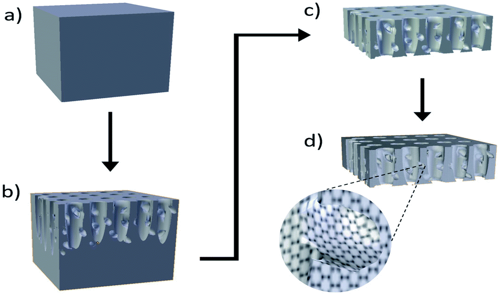
GPSi-nCs consist of a mPSi free-standing membrane whose pore and external surface is covered with graphene. The mPSi free-standing membranes were fabricated by electrochemical etching of highly p-doped (0.01–0.02 Ω cm) Si (100) substrate placed into a single bath cell filled with hydrofluoric acid (49%) and ethanol 1![[thin space (1/6-em)]](https://www.rsc.org/images/entities/char_2009.gif) :1 (v/v) and processed following a protocol described in detail elsewhere.19 A 100 mA cm−2 pulsed current density was used during anodization. In order to detach the porous layer from the mother wafer, the first electrolyte was replaced by a diluted solution made up of hydrofluoric acid (49%) and ethanol 1:3 (v/v). A 220 mA cm−2 current density was used to release the mPSi membrane from the mother wafer. A graphene coating was formed on mPSi specific surface using a Chemical Vapor Infiltration (CVI) process. First, the furnace was purged with argon to limit the formation of native oxides within the mPSi matrix. Next, the deposition was performed via an infiltration step realized at 100 °C for 40 min with a continuous flow of argon, hydrogen and acetylene. Finally, the temperature was increased, and deposition occurred for 40 min. In this work, samples were produced at four graphene deposition temperatures: 750 °C, 800 °C, 850 °C and 920 °C. Fig. 1 shows a schematic of the GPSi-nCs preparation process. Thermally annealed (TA) mPSi samples were also produced for reasons discussed in the following sections. The annealing phase was achieved at 750 °C, 850 °C and 880 °C respectively under argon atmosphere to prevent oxidation of uncarbonized mPSi membranes. Cross-sectional observations using scanning electron microscopy (Zeiss LEO Supra 1530 VP microscope) was used to evaluate the morphology of our mesoporous structures.
:1 (v/v) and processed following a protocol described in detail elsewhere.19 A 100 mA cm−2 pulsed current density was used during anodization. In order to detach the porous layer from the mother wafer, the first electrolyte was replaced by a diluted solution made up of hydrofluoric acid (49%) and ethanol 1:3 (v/v). A 220 mA cm−2 current density was used to release the mPSi membrane from the mother wafer. A graphene coating was formed on mPSi specific surface using a Chemical Vapor Infiltration (CVI) process. First, the furnace was purged with argon to limit the formation of native oxides within the mPSi matrix. Next, the deposition was performed via an infiltration step realized at 100 °C for 40 min with a continuous flow of argon, hydrogen and acetylene. Finally, the temperature was increased, and deposition occurred for 40 min. In this work, samples were produced at four graphene deposition temperatures: 750 °C, 800 °C, 850 °C and 920 °C. Fig. 1 shows a schematic of the GPSi-nCs preparation process. Thermally annealed (TA) mPSi samples were also produced for reasons discussed in the following sections. The annealing phase was achieved at 750 °C, 850 °C and 880 °C respectively under argon atmosphere to prevent oxidation of uncarbonized mPSi membranes. Cross-sectional observations using scanning electron microscopy (Zeiss LEO Supra 1530 VP microscope) was used to evaluate the morphology of our mesoporous structures.
 |
| | Fig. 1 Schematic of sample preparation process: (a) p-doped bulk silicon, (b) mesoporous silicon on bulk silicon after electrochemical etching, (c) free-standing mesoporous silicon membrane detached from mother substrate, (d) graphene-mesoporous silicon nanocomposites. | |
Micro-Raman measurements were made at room temperature using a He–Ne laser at 632.8 nm in the backscattering geometry. The laser power was kept constant at ∼1.3 mW and a 50× microscope objective focused the laser beam on a 3 μm spot diameter on the surface of the sample. The scattered light was directed towards a Labram-800 Raman spectrometer and detected using a nitrogen-cooled charge coupled device (CCD).
The THz time-domain spectroscopy (TDS) setup was coupled to a Ti:sapphire oscillator that delivers 70 fs laser pulses at a 82 MHz repetition rate. The wavelength of the laser pulses was centered at 790 nm. THz radiation was emitted using a semi-insulating GaAs photoconductive antenna triggered by short laser pulses. The excitation beam was chopped at 1350 Hz. The THz pulses transmitted through the test sample was detected by electro-optic sampling in a 0.5 mm-thick ZnTe crystal. The probing beam was polarized parallel to the THz beam and the electro-optic signal was measured using a lock-in amplifier. All THz measurements were done at room temperature in a water vapor free environment.
Photoluminescence measurements were carried out at room temperature using a 1 m-spectrometer (SPEX model) equipped with cooled photomultiplier tube (Hamamatsu R2658 model). A 532 nm semiconductor laser diode providing ∼20 mW was used as an excitation source and the excitation beam was focused onto the sample surface on a spot diameter of ∼100 μm. The PL signals were recorded using a modulated excitation beam at 300 Hz and a lock-in detection.
Results and discussions
Structural characterization
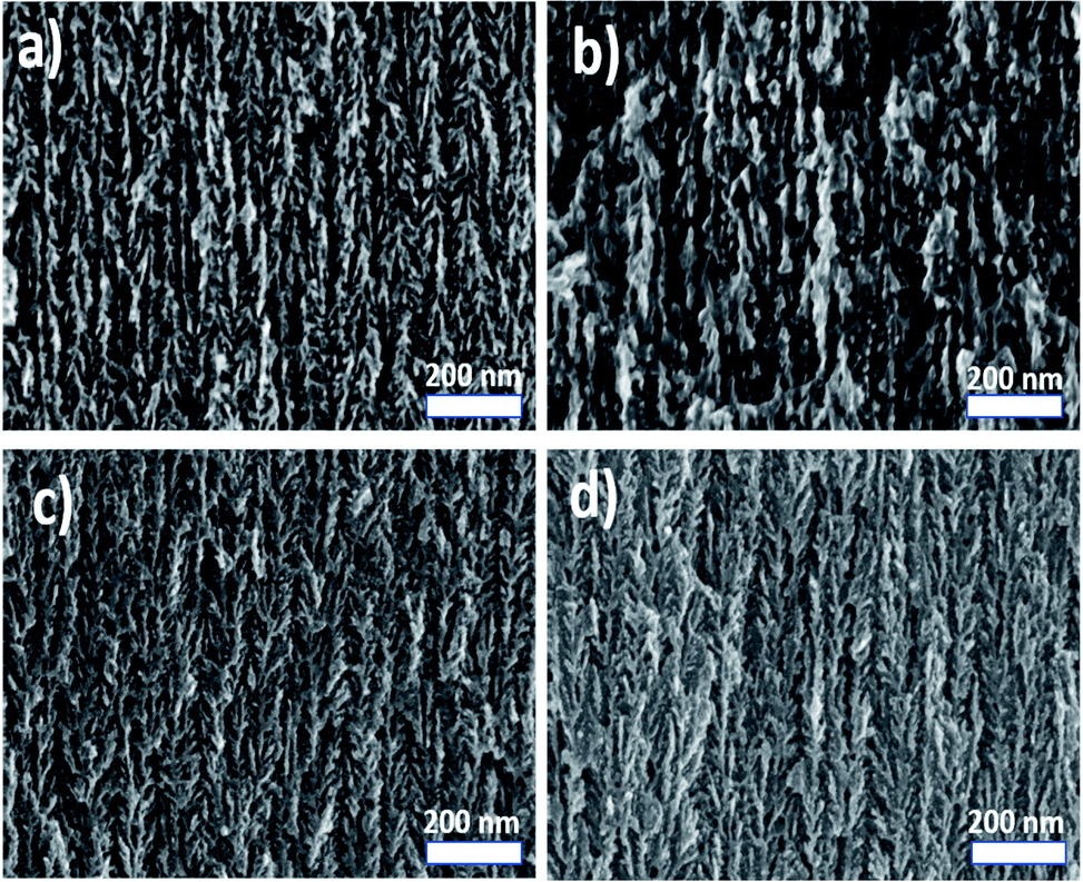
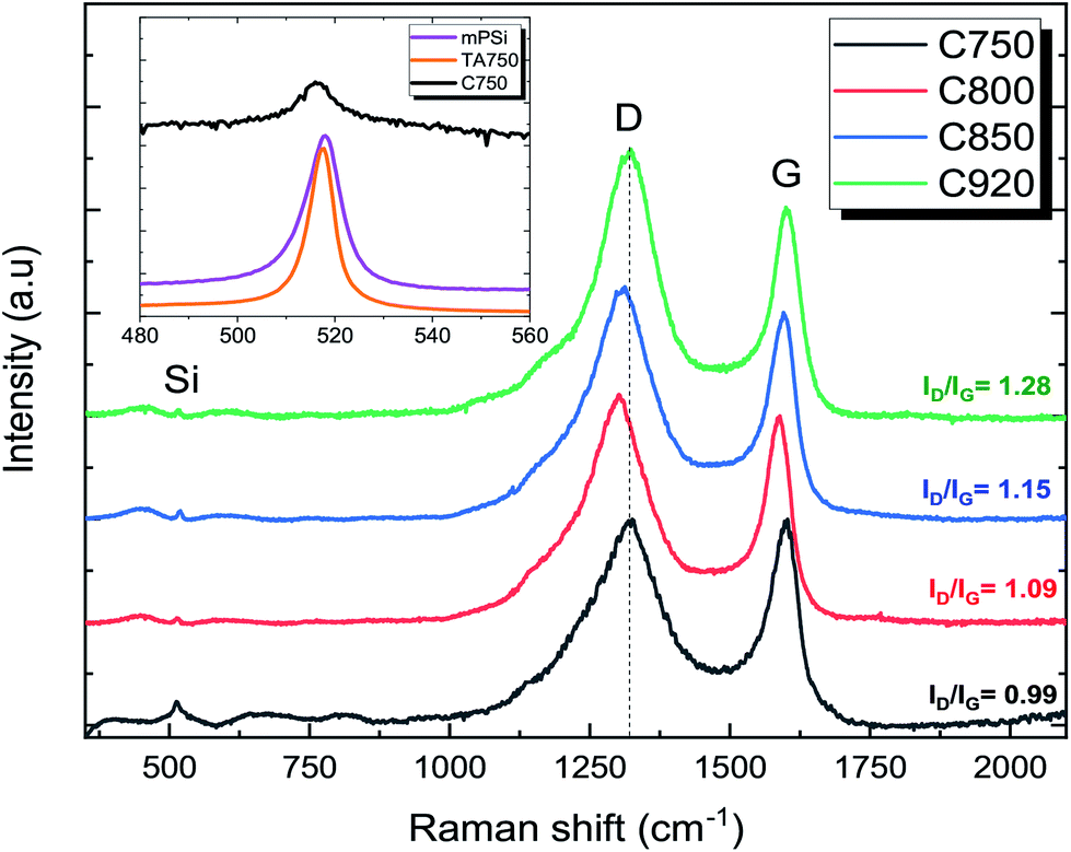
Fig. 2 shows scanning electron microscopy (SEM) cross-sectional images of free-standing mPSi, TA mPSi and GPSi-nCs samples. The average nanocrystallites size and pore diameters were estimated to 6 nm and 17 nm, respectively. The micrographs provide clear evidence of modified surface morphology after thermal annealing process. The surface irregularities are due to fluctuations in the shape and size of the nanocrystallites. Mesoporous materials have very large specific surface compared to bulk. A large portion of atoms in mesoporous compounds are surface atoms with significantly higher mobility at high temperatures compared to bulk atoms.24 Therefore, thermal annealing allows the diffusion of atoms on the surface and promotes the formation of larger nanocrystallites. However, the morphology of the mesoporous structure is conserved when graphene coating is deposited at a higher temperature. Therefore, the graphene coating stabilizes the walls of mesoporous silicon from thermal diffusion processes. Raman spectra of GPSi-nCs illustrated in Fig. 3 show the signature of few-layer graphene or graphene-like carbon with the D and G bands centered at 1320 cm−1 and 1598 cm−1, respectively. The G band is related to first order Raman scattering and is associated with doubly degenerate phonons (iTO and LO) near the center of the Brillouin zone. This band is related to C–C bond stretching and is the main Raman signature of all sp2 carbon systems. For relatively pure graphene, this band usually appears near 1560 cm−1. The D band, usually appearing at around 1350 cm−1, have been attributed to a second order Raman scattering process involving one iTO phonon. It is a breathing mode from sp2 carbon rings that is active only when the ring is adjacent to a graphene edge or a defect.25–27 Another Raman active mode related to C–C bonds between sp3 hybridized carbon atoms of cubic structure also gives a signature at around 1330 cm−1.28,29 For our graphene-like material, both of these vibrational modes might contribute to the intensity of this Raman band, that is designated as the D band, regardless of the nature of the vibration mode. The relative intensity of these two main bands (D and G) is somehow related to the structural quality of our graphene-like films. In relatively pure graphene, the ID/IG value is less than 0.3. The measured ID/IG values are 0.99, 1.09, 1.15 and 1.28 respectively for our C750, C800, C850 and C920 samples. The large values of ID/IG are characteristics of a poor few-layer graphene 2D crystallinity. This ratio increases with graphene deposition temperature indicating an increased amount of sp3 hybridized carbon as the films grow.
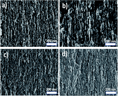 |
| | Fig. 2 Scanning electron microscopy (SEM) cross section images: (a) mPSi membrane, (b) thermally annealed mPSi at 750 °C (TA750), (c) GPSi-nC formed at 750 °C (C750), (d) GPSi-nCs formed at 850 °C (C850). | |
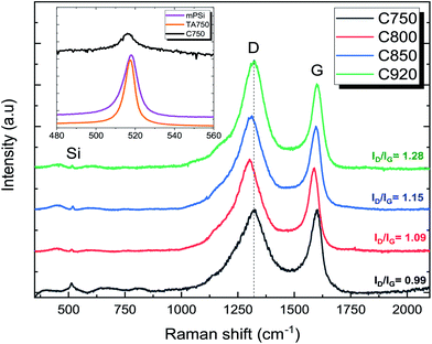 |
| | Fig. 3 Raman spectra of GPSi-nCs presents D and G bands characteristic of graphene. Spectra are vertically shifted for clarity. The inset in the figure illustrates the Si band for mPSi, TA750 and C750 samples. | |
Raman spectra taken at different spots on the samples surface as well as Raman spectra of previously reported GPSi-nCs show similar values of ID/IG ratio to ours, owing to a relatively uniform graphene coating. Based on gravimetric analysis, ref. 20 estimated the coating thickness to 2–3 monolayers for graphene deposition temperature between 650 °C and 800 °C. The inset in Fig. 3 illustrates a well-defined silicon peak at 517 cm−1 corresponding to the free-standing mPSi sample. For the C750 sample, new graphene-related bands emerge causing a strong reduction of the Si LO phonon peak which is redshifted and broader compared to the one in free mesoporous samples. The slight shift observed in the position of this peak (−1.22 cm−1) is a good indicator of tensile stress exerted on Si nanocrystallites. The stress is probably induced by the graphene coating.
THz dielectric properties
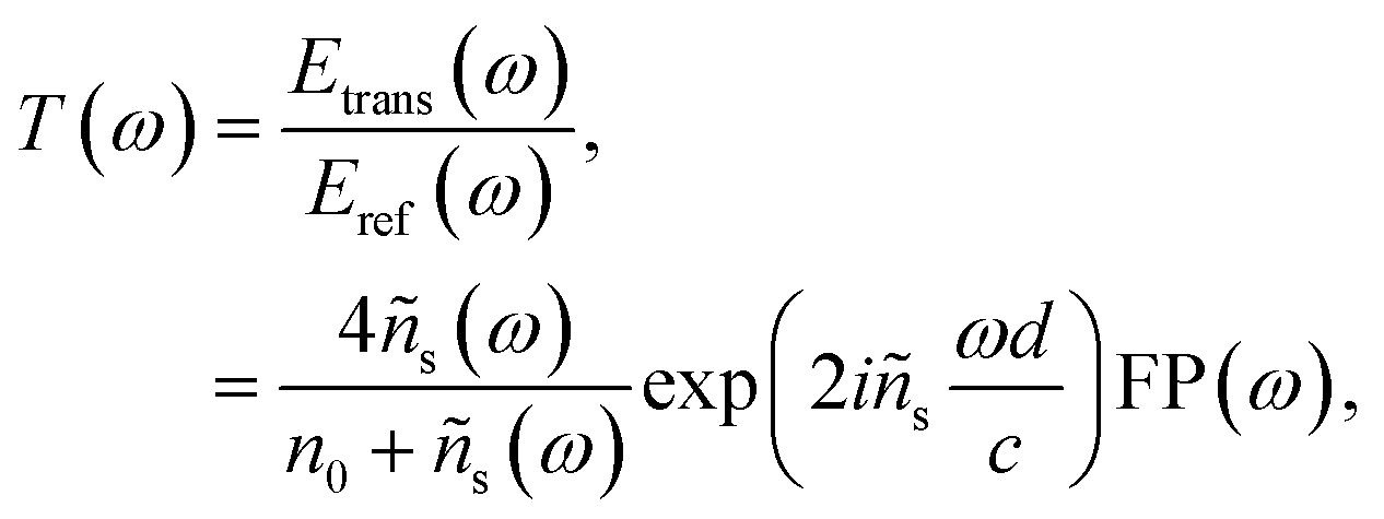
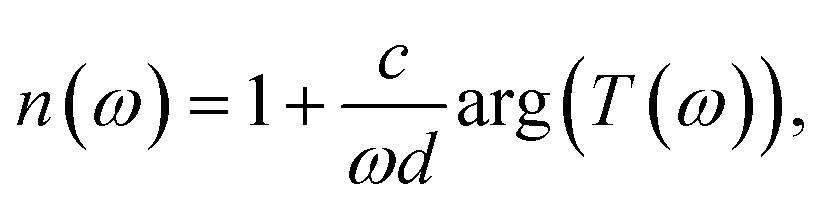
THz TDS is a powerful technique to investigate the far infrared dielectric properties of semiconductors. In dielectric, bound charges absorb the low-energy THz photons and get promoted towards higher vibrational modes. In metals or doped semiconductors, it is the free charges that absorb THz photons to undergo motion. In transmission mode, a THz pulse transmitted through the sample of refractive index n and thickness d undergoes a temporal delay given by (n−1)d/c where c is the speed of light in vacuum. This pulse will also undergo multiple reflections at the air/sample boundaries leading to the formation of several echoes. In optically thin media, the echo delay 2nd/c is small enough such that all echoes appear within the first THz pulse. This mechanism generates Fabry–Perot artifacts in the complex transfer function of the sample that can significantly perturb the real and imaginary parts of the dielectric function. If ñs(ω) = n(ω) + i(c/2ω)α(ω), is the complex refractive index of the sample, the complex transfer function T(ω) of the THz pulses at normal incidence can be expressed as:| | 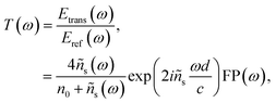 | (1) |
| |  | (2) |
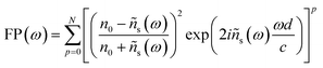
where FP(ω) is the Fabry–Perot function, N is the number of echoes contained in the temporal trace of the THz pulse and n0 is the refractive index of the reference environment (n0 ∼ 1) in which the THz pulse travels. Here we assume the porous nanocomposites substrate to be dielectrics, such that:| | 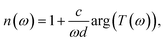 | (3) |
| |  | (4) |
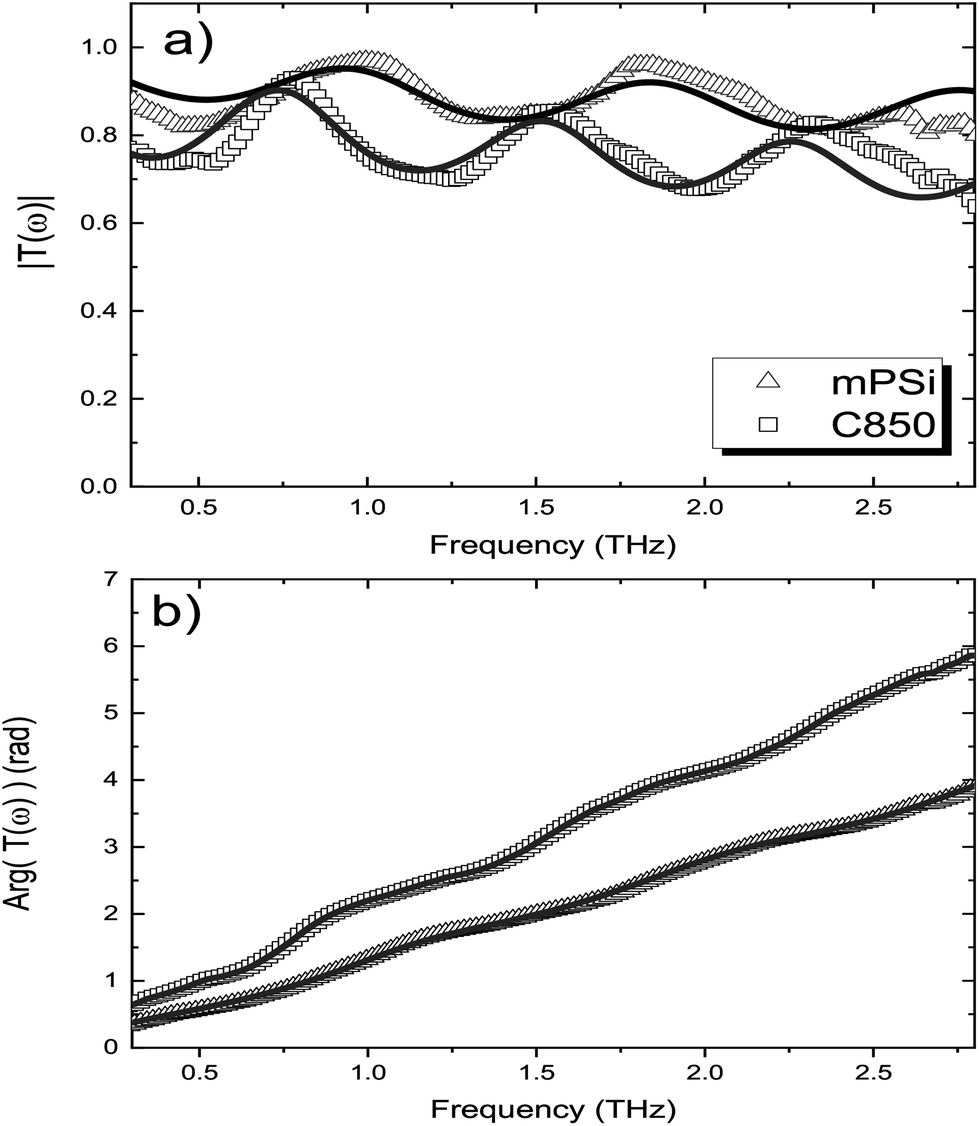
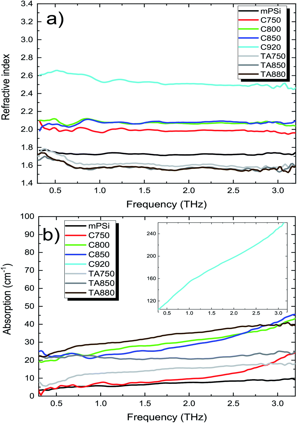
Since the work of Duvillaret et al.,30 error minimization algorithms have been widely used to cancel Fabry–Perot oscillations in the frequency dependent refractive index and absorption coefficient of optically thin samples. In this work, we use a homemade program inspired from a recent work31 to remove the contribution of the Fabry–Perot oscillations present in the |T(ω)| and arg[T(ω)] curves in order to recover the correct dielectric properties n(ω) and α(ω) of the film. Fig. 4 illustrates the amplitude (a) and the phase (b) of the transfer function for the mPSi and C850 samples. The solid lines correspond to the best fits to the data curves obtained using eqn (1) and (2). The same procedure has been used to extract the frequency-dependent dielectric properties of our different samples. These results are summarized in Fig. 5. The refractive index n(ω) shows very little dispersion with values ranging between n0 = 1 for air and nSi ∼ 3.42 for bulk silicon. The variation of this value from one sample to the other must be related to the nature and thickness of the native oxide on the Si nanocrystallites as well as the level of pore filling by the graphene or carbonized coating. On the other hand, Fig. 5b shows a slight increase in the absorption coefficient as a function of frequency, for all samples. In addition, the level of absorption increases with the annealing temperature and with the graphene deposition temperature. The interpretation of these behaviors requires a good description of the various interactions between the material and the THz radiation. Let us first mention that there are no free charges in our mPSi materials. In addition, electrical measurements performed parallel to the surface of the membranes (direction of the THz field in our experiments) show negligible conductivity for all our samples even for the ones with a graphene-like coating. Therefore, the dielectric properties of our samples can be well described by the Lorentz oscillator model. The refractive index and the absorption coefficient get bigger as the density of electric dipoles, contained within the nanocrystallites or at their interfaces increases. The functions n(ω) and α(ω) depend both on the number of dipoles and the position of their resonance frequency. For samples annealed at high temperature, the results suggest that the treatment leads to a partial desorption of atoms in the oxide/passivation layer surrounding the nanocrystallites. The loss of material will directly affect the density of electric dipoles resulting in a reduction of the refraction index, while the appearance of dangling bonds on the surface of the nanocrystallites could lead to an increase of the low-frequency absorption due to a change in the resonant frequencies of these new dipolar oscillators.
 |
| | Fig. 4 Amplitude (a) and phase (b) of the complex transfer function. The solid lines correspond to the best fits to the data using eqn (1) and (2). | |
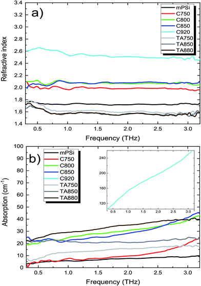 |
| | Fig. 5 (a) Refractive index of samples increasing with graphene deposition temperature. (b) Evolution of the samples absorption coefficient with frequency. The low mPSi absorption coefficient (<10 cm−1) within 0.3–3 THz range is consistent with literature.10 The absorption level increases with graphene deposition temperature. | |
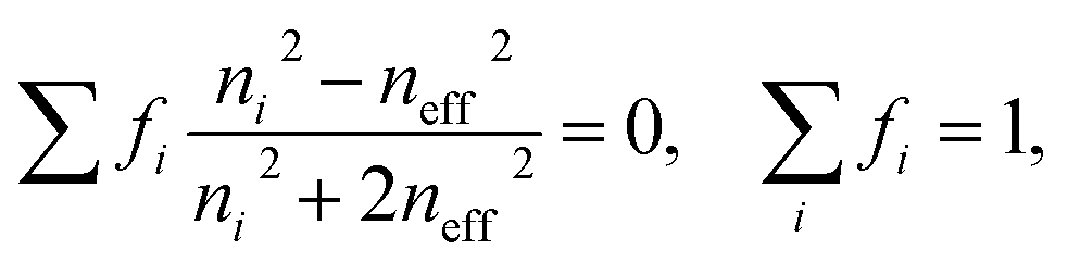
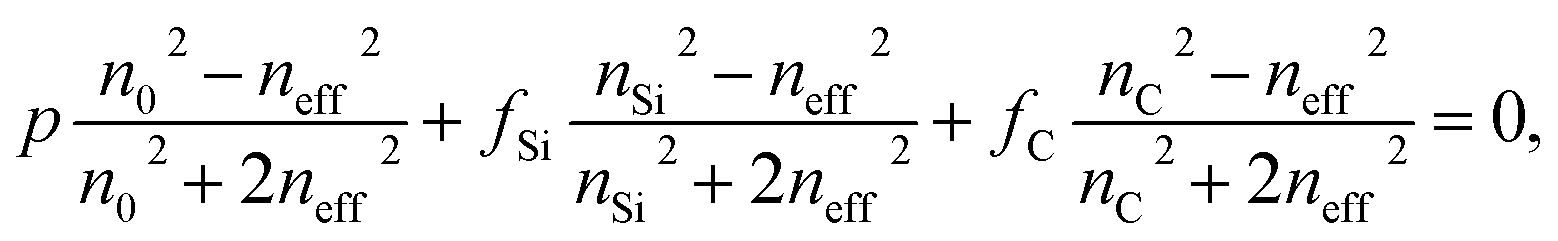
For the composite materials, the refractive index increases as the deposition temperature increases. This behavior can be explained by carbon diffusion within the pores of the mPSi matrix. At temperatures >700 °C, the carbon atoms are sufficiently mobile on the walls of the pores to favor the formation of graphene-like materials. The dielectric properties of each constituent of the nanocomposite materials can be evaluated using an effective medium theory (EMT).32 The most widely used EMTs are Maxwell-Garnett (MG) and Bruggeman (BR) models. MG theory assumes spherical inclusions much smaller than the pore sizes and uniformly distributed within a given matrix. However, this model does not suit for our samples since the average pore size and nanocrystallite diameter are comparable. The BR theory on the other hand is more appropriate for heterogeneous composites with a wider range of inclusion sizes. It is mathematically expressed as:
| | 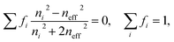 | (5) |
where
neff is the effective refractive index of the composite,
ni and
fi are the intrinsic refractive index and volume fraction of the
ith inclusion respectively. We use the following expanded Bruggeman formula
| | 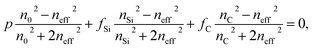 | (6) |
to evaluate the porosity
p of the membranes. In this equation
n0 = 1 is the refractive index of the pores (air),
nSi and
fSi are the refractive index and volume fraction of Si respectively, while
nC and
fC are the refractive index and volume fraction of graphene. For the sake of simplicity, we neglect the influence of a thin oxide layer on the effective refractive index of the composite material for all samples. Values of
p and
fC are estimated using
eqn (6) and the experimental values of
neff at 1 THz are evaluated from
Fig. 5a. In this procedure, we assume the refractive indices of the few-layer graphene coating and that of Si nanocrystallites to be
nC = 101 (
ref. 33) and
nSi = 3.42, respectively. The extracted values are given in
Table 1. Results show that the porosity decreases while the carbon content increases as the graphene deposition temperature increases. The value of the effective refractive index goes from 1.72 for the mPSi sample to 2.53 for GPsi-nC sample made at 920 °C. mPSi exhibits very small absorption coefficient (<10 cm
−1) within the 0.3–3 THz as reported by previous works.
10,11 The increasing trend of the absorption coefficient with frequency could result from Si phonon bands at 3.66 THz, 4.11 THz, 11.17 THz and even stronger bands at 16.99 THz and 18 THz.
34 The comparison of the absorption curves in
Fig. 5b shows that it is the annealing temperature or the graphene deposition temperature that mostly affects the level of absorption. For these two types of samples, the breaking of the Si–Si and Si–H bonds at the surface seems to create dangling bonds or harmful defects for the THz absorption in the 0.3 to 3 THz range. Previous work has shown that the deposition of a graphene-like coating stabilized the structure of the Si nanocrystallites,
19 but these new results indicate that the process still needs to be optimized in order to limit the presence of these surface defects which significantly increase the THz absorption level.
Table 1 Impact of graphene deposition temperature on refractive index and porosity as determined by Bruggeman model (eqn (6))
| Samples |
Temp (°C) |
n
eff
|
Porosity p (%) |
f
C (%) |
| mPSi |
— |
1.72 |
63.5 |
— |
| C750 |
750 |
1.96 |
61.5 |
7.7 |
| C800 |
800 |
2.02 |
59.8 |
9.4 |
| C850 |
850 |
2.07 |
59.7 |
9.5 |
| C920 |
920 |
2.53 |
54.5 |
14.7 |
Photoluminescence
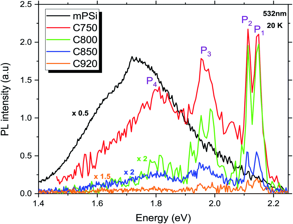
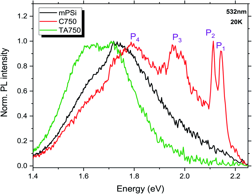
Low temperature (20 K) photoluminescence of mPSi and GPSi-nCs are shown in Fig. 6. A broad PL band centered at 1.75 eV is observed for the mPSi sample. The energy of the emitted photons is higher than the bulk Si indirect band gap and this is due to quantum confinement in the Si nanocrystallites.4,13,14 PL spectra of GPSi-nCs show a series of emission bands at higher energies (from 1.79 to 2.2 eV) common to all samples. Moreover, the PL signal is drastically reduced as the graphene deposition temperature increases. This PL quenching effect is explained by an increasing density of nonradiative recombination centres in these samples. These defects are mainly surface traps associated with Si–Si bond breaking and Si-impurity complex formation.8,9,17 In order to better understand the origin of the high-energy emission bands observed for the graphene-coated films, we compare in Fig. 7 the PL spectra of three samples: the untreated mPSi film, the mPSi film annealed at 750 °C, and the nanocomposite material made at 750 °C. The broad luminescence band observed for the mPSi and TA750 samples is characteristic of a large size distribution of Si nanocrystallites. The spectra show the presence of two dominant bands, indicating a bimodal size distribution of nanocrystallites. These PL spectra show that annealing has the effect of red-shifting these two emission bands. This observation is consistent with SEM results which show that the size of the nanocrystallites increases after the thermal annealing treatment. The appearing of a lower energy emission may also result from an energy transfer via charge carrier diffusion or Förster resonance between smaller Si nanocrystallites and larger nanocrystallites where the lower energy radiative recombination is expected. For the C750 sample, the PL main broad emission band appears to be blue-shifted with respect to the same PL band of the mPSi and TA750 samples. This blue shift can be explained by strain exerted upon Si nanocrystallites that induce an additional carrier confinement. A pioneer work established that few-layer graphene has a negative linear thermal expansion coefficient (TEC) that can be as large as −8 × 10⁻⁶ K−1 for monolayers.35 Through Raman spectroscopy it was found that upon heating (cooling) of a few-layer graphene sample grown on SiO2 substrate, the graphene film undergoes compressive (tensile) stress as the SiO2 substrate expands (contracts). For our GPSi-nC samples, it appears that the growth of graphene at high temperature and the cooling of the sample leads to a net stress upon the Si nanocrystallites which is the cause of the blue-shift of the P4 emission band.
 |
| | Fig. 6 PL spectra of mPSi and GPSi-nCs excited at 532 nm. Luminescence bands on the high energy side of the mPSi emission band emerge from carbonization. | |
 |
| | Fig. 7 PL spectra of three different samples: a mPSi film, a thermally annealed mPSi film (TA750), and a GPSi-nCs film produced at 750 °C (C750). For the C750 sample, the designated P1, P2, P3 and P4 emission bands are common for each of our graphene-coated film. | |
Three other emission bands, labeled P1, P2 and P3, are visible at 2.14 eV, 2.11 eV and 1.95 eV, respectively. The broad P3 band is attributed to carrier or exciton recombination within Si nanocrystallites of smaller sizes compared to the nanocrystallites in the mPSi sample. This could suggest that the diffusion length of the photocarriers is severely reduced in our nanocomposite materials, which prevents the carriers or excitons from reaching the lower energy regions corresponding to the larger nanocrystallites. This observation could also be explained by the altering of a Förster energy transfer between close Si nanocrystallites by the graphene coating.36 In this case, the perturbation of the dipole–dipole interaction between nanocrystallites would decouple smaller nanocrystallites from larger ones, hence, leading to a relative increase of the PL signal coming from regions of high confinement in small nanocrystallites (P3 and P4 bands). On the other hand, the P1 and P2 are less likely to be associated with luminescence from Si nanocrystallites as they appear far away (320–350 meV) from the Si nanocrystallite emission band. In addition, these emission bands are very narrow and appear only for the graphene coated samples. These observations suggest that they are associated with the radiative recombination of carriers or excitons in a thin SixC1−x37,38 layer present at the Si/graphene interfaces. In fact, Si–C like bonds have already been observed in thermally carbonized porous silicon.21,39–41 Nevertheless, the narrow width of P1 and P2 emission bands as well as their very small intensity drop with temperature (see ESI†) are also consistent with radiative recombination of excitons bound to deep defects in SiC.42 These defects are most likely Si vacancy related point defects in SiC and are well known for their good optical stability.
Conclusions
In summary, the optical, structural and high-frequency dielectric properties of a series GPSi-nCs grown at different temperatures were investigated using Raman, photoluminescence and THz time-domain spectroscopy. It is found that the graphene coating stabilizes the morphology of the Si nanocrystallites in the nanocomposites as opposed to uncoated samples. THz spectroscopy results show partial filling of mesopores by carbon and the increase in the amount of ligand bonds with the graphene deposition temperature. Pore filling by carbon atoms was found to significantly tune the refractive index at filling fractions greater than 10% of the nanocomposites volume. Photoluminescence spectroscopy revealed a series of four emission bands in the 1.79–2.2 eV energy range. The main broad bands centered at 1.79 eV and 1.96 eV have been attributed to radiative recombination in Si nanocrystallites of different sizes. The two narrower bands observed at 2.11 eV and 2.14 eV have been tentatively attributed to excitonic recombinations in the SiC film formed at the Si/C interfaces. The integrated PL intensity over all these bands decreases rapidly as the carbonized films filled the pores of the mPSi film, which is attributed to the growing density of nonradiative recombination centres formed at these interfaces. Our results stress the critical role of the graphene coating on the structural and THz dielectric properties of GPSi-nCs and the impact of the SiC thin film formed at the Si/C interface on their optical properties. The possibility to further engineer surface (functionalization or passivation) as well as their stable mechanical and optical properties make GPSi-nCs potential good candidates for optical sensing applications. Low absorption of GPSi-nCs at THz frequencies and the relatively large electron mobility exhibited by porous silicon make GPSi-nCs interesting materials for optoelectronic applications.
Conflicts of interest
There are no conflicts to declare.
Acknowledgements
This work is supported financially by NSERC and FRQNT (Québec). The authors would like to thank G. Laliberté for technical support, M. Mbodji for valuable help on Fabry–Perot cancellation algorithm needed for extracting THz dielectric properties of our films, and A. Dupuy for valuable discussions on the fabrication aspects of the mPSi membranes. The authors also appreciate discussion with B. Ilahi on the origin of the GPSi-nCs PL bands.
Notes and references
- H. Sohn, S. Létant, M. J. Sailor and W. C. Trogler, J. Am. Chem. Soc., 2000, 122, 5399–5400 CrossRef CAS.
- N. Massad-Ivanir, G. Shtenberg, N. Raz, C. Gazenbeek, D. Budding, M. Bos and E. Segal, Sci. Rep., 2016, 6, 38099 CrossRef CAS PubMed.
- Kenry, J. C. Yeo and C. T. Lim, Microsyst. Nanoeng., 2016, 2, 16043 CrossRef CAS PubMed.
-
L. Canham, Handbook of Porous Silicon, Springer, 2014, pp. 1–1017 Search PubMed.
- G. Lammel, S. Schweizer and P. Renaud, Sens. Actuators, A, 2001, 92, 52–59 CrossRef CAS.
- M. Ge, J. Rong, X. Fang and C. Zhou, Nano Lett., 2012, 12, 2318–2323 CrossRef CAS PubMed.
- A. Douglas, N. Muralidharan, R. Carter, K. Share and C. L. Pint, Nanoscale, 2016, 8, 7384–7390 RSC.
- R. Schwarz, F. Wang, M. Ben-Chorin, S. Grebner, A. Nikolov and F. Koch, Thin Solid Films, 1995, 255, 23–26 CrossRef CAS.
- R. Tomasiunas, I. Pelant, J. Kocka, P. Knápek, R. Lévy, P. Gilliot, J. B. Grun and B. Hönerlage, J. Appl. Phys., 1996, 79, 2481–2486 CrossRef CAS.
- J. Knab, X. Lu, F. Vallejo, G. Kumar, T. Murphy and L. Michael Hayden, Opt. Mater. Express, 2014, 4, 300–307 CrossRef CAS.
- S.-Z. A. Lo, A. M. Rossi and T. E. Murphy, Phys. Status Solidi A, 2009, 206, 1273–1277 CrossRef CAS.
- X. Chen, D. Uttamchandani, C. Trager-Cowan and K. P. O'Donnell, Semicond. Sci. Technol., 1993, 8, 92 CrossRef CAS.
- L. Canham, Appl. Phys. Lett., 1990, 57, 1046–1048 CrossRef CAS.
- L. Canham, T. Cox, A. Loni and A. Simons, Appl. Surf. Sci., 1996, 102, 436–441 CrossRef CAS.
- Y. Qu, L. Liao, Y. Li, H. Zhang, Y. Huang and X. Duan, Nano Lett., 2009, 9, 4539–4543 CrossRef CAS PubMed.
- A. I. Mabilangan, L. P. Lopez, M. A. B. Faustino, J. E. Muldera, N. I. F. Cabello, E. S. Estacio, A. A. Salvador and A. S. Somintac, Superlattices Microstruct., 2016, 100, 892–899 CrossRef CAS.
- A. Zakar, R. Wu, D. Chekulaev, V. Zerova, W. He, L. Canham and A. Kaplan, Phys. Rev. B, 2018, 97, 155203 CrossRef CAS.
- V. Lehmann and U. Gösele, Appl. Phys. Lett., 1991, 58, 856–858 CrossRef CAS.
- A. R. Boucherif, A. Boucherif, G. Kolhatkar, A. Ruediger and R. Arès, Small, 2017, 13, 1603269 CrossRef PubMed.
- G. Kolhatkar, A. Boucherif, A. R. Boucherif, A. Dupuy, L. G. Fréchette, R. Arès and A. Ruediger, Nanotechnology, 2018, 29, 145701 CrossRef PubMed.
- J. Salonen and E. Mäkilä, Adv. Mater., 2018, 30, 1703819 CrossRef PubMed.
-
S. Muto, A. Vasin, Y. Ishikawa, N. Shibata, J. Salonen and V. P. Lehto, PRICM 6, 2007, pp. 1127–1130 Search PubMed.
- J. Buriak, Chem. Rev., 2002, 102, 1271–1308 CrossRef CAS PubMed.
- G. Müller, M. Nerding, N. Ott, H. P. Strunk and R. Brendel, Phys. Status Solidi A, 2003, 197, 83–87 CrossRef.
- L. Malard, M. Pimenta, G. Dresselhaus and M. Dresselhaus, Phys. Rep., 2009, 473, 51–87 CrossRef CAS.
- A. C. Ferrari, Solid State Commun., 2007, 143, 47–57 CrossRef CAS.
- A. Jorio, ISRN Nanotechnol., 2012, 2012, 234216 Search PubMed.
- L. Oakes, A. Westover, J. W. Mares, S. Chatterjee, W. R. Erwin, R. Bardhan, S. M. Weiss and C. L. Pint, Sci. Rep., 2013, 3, 3020 CrossRef PubMed.
- T. Jawhari, A. Roid and J. Casado, Carbon, 1995, 33, 1561–1565 CrossRef CAS.
- L. Duvillaret, F. Garet and J.-L. Coutaz, IEEE J. Sel. Top. Quantum Electron., 1996, 2, 739–745 CrossRef CAS.
- A. Taschin, P. Bartolini, J. Tasseva and R. Torre, Measurement, 2017, 118, 282–288 CrossRef.
- V. Markel, J. Opt. Soc. Am. A, 2016, 33, 1244–1256 CrossRef PubMed.
- I.-T. Lin, J.-M. Liu, K.-Y. Shi, P.-S. Tseng, K.-H. Wu, C.-W. Luo and L.-J. Li, Phys. Rev. B: Condens. Matter Mater. Phys., 2012, 86, 235446 CrossRef.
- B. A. Weinstein and G. J. Piermarini, Phys. Rev. B: Solid State, 1975, 12, 1172–1186 CrossRef CAS.
- D. Yoon, Y.-W. Son and H. Cheong, Nano Lett., 2011, 11, 3227–3231 CrossRef CAS PubMed.
- T.-Q. Nguyen, J. Wu, V. Doan, B. J. Schwartz and S. H. Tolbert, Science, 2000, 288, 652–656 CrossRef CAS PubMed.
- H. W. Shim, K. C. Kim, Y. H. Seo, K. S. Nahm, E.-K. Suh, H. J. Lee and Y. G. Hwang, Appl. Phys. Lett., 1997, 70, 1757–1759 CrossRef CAS.
- J. Fan, X. Wu and P. K. Chu, Prog. Mater. Sci., 2006, 51, 983–1031 CrossRef CAS.
- Y. Seo, H. Cheon and D. Choi, J. Mater. Sci. Lett., 1998, 17, 313–315 CrossRef CAS.
- J. Salonen, E. Laine and L. Niinistö, J. Appl. Phys., 2002, 91, 456–461 CrossRef CAS.
- A. V. Vasin, P. N. Okholin, I. N. Verovsky, A. N. Nazarov, V. S. Lysenko, K. I. Kholostov, V. P. Bondarenko and Y. Ishikawa, Semiconductors, 2011, 45, 350–354 CrossRef CAS.
- J. R. Weber, W. F. Koehl, J. B. Varley, A. Janotti, B. B. Buckley, C. G. Van de Walle and D. D. Awschalom, J. Appl. Phys., 2011, 109, 102417 CrossRef.
Footnote |
| † Electronic supplementary information (ESI) available. See DOI: 10.1039/c9na00502a |
|
| This journal is © The Royal Society of Chemistry 2020 |
Click here to see how this site uses Cookies. View our privacy policy here. 
 Open Access Article
 This Open Access Article is licensed under a Creative Commons Attribution-Non Commercial 3.0 Unported Licence
 *abc,
Stéphanie
Sauze
bc,
Abderraouf
Boucherif
bc,
Richard
Arès
*abc,
Stéphanie
Sauze
bc,
Abderraouf
Boucherif
bc,
Richard
Arès