DOI:
10.1039/D0MH00250J
(Communication)
Mater. Horiz., 2020,
7, 1613-1622
Solution-processed one-dimensional CsCu2I3 nanowires for polarization-sensitive and flexible ultraviolet photodetectors†
Received
13th February 2020
, Accepted 1st April 2020
First published on 2nd April 2020
Abstract
Recently, much progress has been made in polarization-sensitive photodetectors based on the newly-emerging metal-halide perovskites. However, compared to extensive work on visible/infrared-light photodetection, polarization-sensitive perovskite photodetectors targeted at the ultraviolet (UV) region have not been reported. In addition, most of the previously reported photodetectors concentrated on lead-halide perovskites, but the lead-toxicity and poor stability severely restricted their practical applications. In this study, for the first time, one-dimensional CsCu2I3 nanowires (NWs) were used as the light absorber to fabricate a polarization-sensitive UV photodetector because of their electric and optical anisotropy of the asymmetric structure and external morphology anisotropy, and a high photocurrent anisotropy ratio of ∼3.16 was achieved. Owing to the high crystallinity of the CsCu2I3 NWs, the device exhibits remarkable photodetection ability with a photoresponsivity of ∼32.3 A W−1, a specific detectivity of 1.89 × 10¹² Jones, and a fast response speed of 6.94/214 μs. Moreover, such a device fabricated on a flexible substrate shows almost no photodetection degradation after extreme bending for 1000 cycles, demonstrating good flexibility and bending endurance. The results obtained highlight the great potential of such copper halides as a stable and environmentally-friendly candidate for polarization-sensitive UV photodetectors, rendering them potentially useful for assembly of optoelectronic systems in the future.
New concepts
Polarization-sensitive ultraviolet (UV) photodetectors are highly desired due to their great significance in many applications. As newly-emerging functional semiconductors, metal-halide perovskites have attracted huge attention in photodetection due to their excellent optoelectronic features. However, the previously reported perovskite polarized photodetectors mainly focused on the visible/infrared-light region, and devices targeted at the UV region have not been reported. Here, for the first time, ternary copper halide CsCu2I3 nanowires were used as the light absorber to achieve polarization-sensitive UV photodetection. By combining the intrinsic anisotropy of the asymmetric structure and external morphology anisotropy of CsCu2I3 nanowires, a record photocurrent anisotropy ratio of ∼3.16 was achieved, and also the shortcomings of lead-toxicity and environmental instability for conventional lead-halide perovskites were overcome effectively. Moreover, such photodetectors fabricated on a flexible substrate demonstrate good flexibility and stability, showing almost no photoresponse degradation after extreme bending for 1000 cycles. The results suggest that the lead-free CsCu2I3 nanowires are potentially an attractive candidate for high-performance polarization-sensitive UV photodetectors compatible for practical applications.
|
Introduction
Recently, polarization-sensitive photodetectors have increasingly attracted research interest because of their significant applications like high-contrast polarizers, optical switches and interconnects, etc.,1,2 which require photoactive materials with outstanding optoelectronic characteristics, and anisotropic crystal structures or morphology. On the one hand, materials with unique anisotropic properties originating from asymmetric crystal structures have always been applied in polarization-sensitive photodetectors, such as black phosphorus,3–5 germanene,6 and antimony selenide.7,8 On the other hand, materials with one-dimensional (1D) morphology can be also used as photoactive materials for polarization-sensitive photodetection, resulting in linear polarization sensitivity.2,9,10 For example, by means of the order-of-magnitude polarization anisotropy of InP nanowires (NWs) resulting from the great dielectric contrast between the NWs and the surrounding environment, Wang et al. demonstrated a polarization-sensitive nanoscale photodetector based on isolated InP NWs.2 A similar polarization-sensitive photoresponse was also observed in an aligned CdSe quantum-wire solid by Singh et al.11
As newly-emerging functional semiconductors, the intrinsically large light absorption coefficient and long charge diffusion length provide metal-halide perovskites with broad prospects for high-performance photodetectors,12–20 and much progress in this field has been witnessed in the past three years.21–24 Very recently, polarization-sensitive photodetectors based on such perovskite materials have attracted much attention.9,25–32 For example, by using the anisotropic geometry of CH3NH3PbI3 NWs, polarization-sensitive light detection was achieved by Tang's and Jiang's groups.9,32 Zhang et al. reported a polarization-dependent photodetector based on CsPbX3 single-crystal NW arrays,25 and the minimum photocurrent appears in the direction perpendicular to the axial direction, while the maximum photocurrent appears when the polarization angle is parallel to the NWs. For the above three studies, the polarization-sensitive photodetection was realized through the external anisotropy of the 1D geometry of perovskite NWs, which is due to the fact that tetragonal CH3NH3PbI3 and cubic CsPbX3 have symmetric crystal structures lacking intrinsic anisotropy. In reality, polarization-sensitive photodetection realized by the intrinsic anisotropy of the asymmetry crystal structure was also proved to be an effective strategy. For example, Ding et al. demonstrated a CH3NH3PbCl3 perovskite single crystal with an anisotropic crystal structure for polarized light detection.26 By using anisotropic orthorhombic CsPbI3 NWs, Zhou et al. fabricated a linearly polarized visible photodetector with a photocurrent anisotropy ratio of 2.68.27 More recently, Ghoshal et al. demonstrated the potential of 2D layered (BA)2PbI4 perovskite NWs with anisotropic crystal structure for polarized light detection.28 But, so far, the previously reported devices have mainly focused on visible/infrared-light detection, and polarization-sensitive perovskite photodetectors targeted at the ultraviolet (UV) region are rarely reported. Moreover, another important factor is that most of the previous studies use conventional lead-halide perovskites, and their environmental instability and toxicity limit their further commercialization.33–35 Thus, it is imperative to search for environmentally stable and lead-free alternatives as the photoactive material targeted at the UV region to solve the above problems.
Herein, we demonstrated a polarization-sensitive UV photodetector based on solution-processed 1D CsCu2I3 NWs. By combining the intrinsic anisotropy of the asymmetric structure and external morphology anisotropy of the CsCu2I3 NWs, a record photocurrent anisotropy ratio of ∼3.16 was achieved among perovskite-based polarized photodetectors. Owing to the high crystallinity of the CsCu2I3 NWs, the device performance is remarkable in terms of a photoresponsivity of ∼32.3 A W−1, a specific detectivity of 1.89 × 10¹² Jones, and a fast response speed of 6.94/214 μs. Moreover, such devices fabricated on a flexible polyethylene terephthalate (PET) substrate demonstrate good flexibility and stability, showing almost no photoresponse degradation after 1000 bending cycles. Given the record polarization sensitivity and high stability, the lead-free copper halides might hold promise for high-performance polarization-sensitive UV photodetectors compatible for practical applications.
Results and discussion
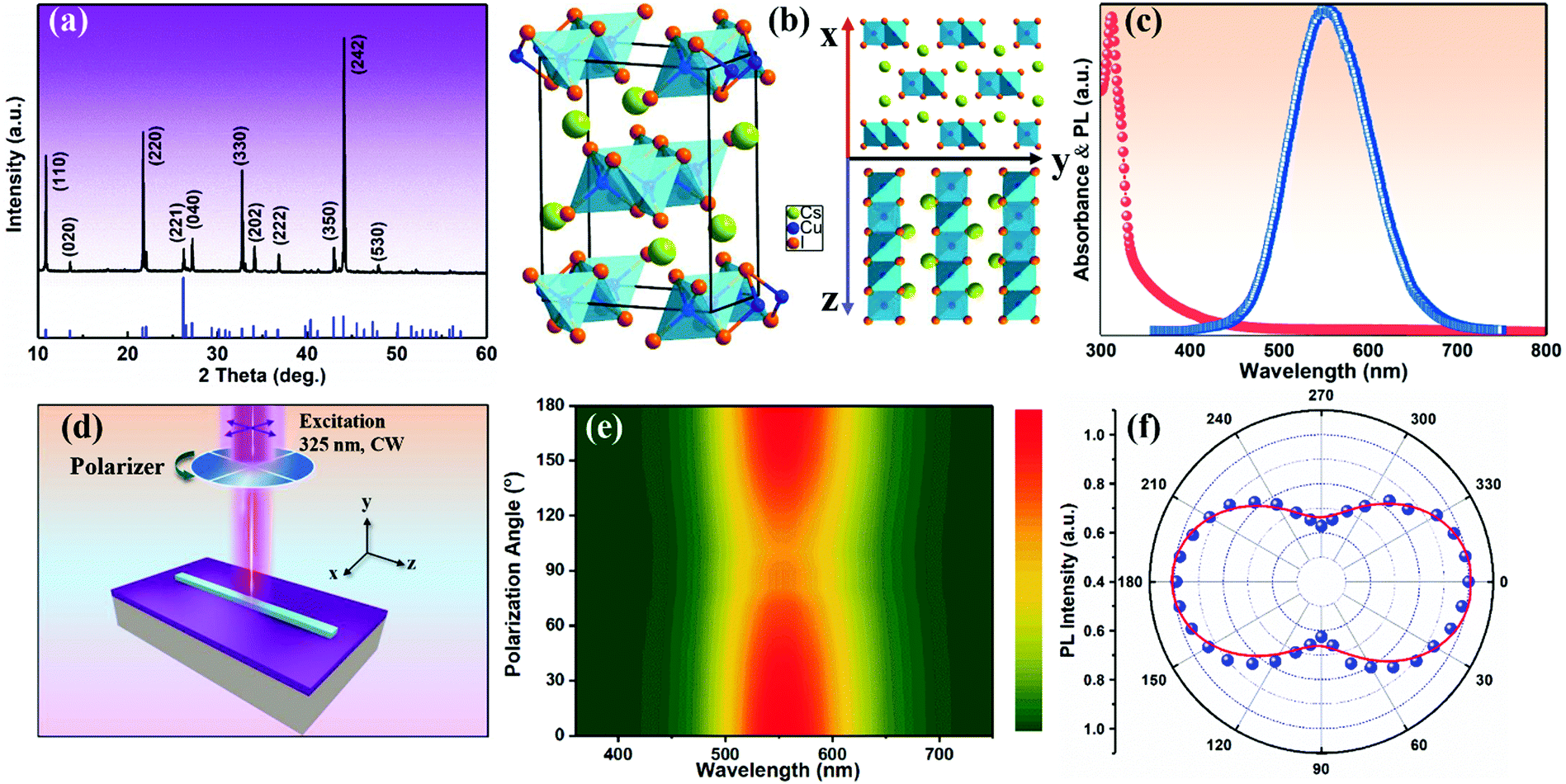
Fig. 1a illustrates the preparation procedures of 1D CsCu2I3 NWs by using antisolvent engineering, as reported for conventional lead-halide perovskites, and diethyl ether was employed as the antisolvent. Note that the diffusion of diethyl ether in acetonitrile will consume some acetonitrile solvent in the precursor solution. Since CsI and CuI cannot dissolve in diethyl ether, the consumption of acetonitrile will increase the concentration of CsI and CuI in the solution. This will result in the crystallization and formation of CsCu2I3 crystals, and detailed parameters are shown in the Experimental section. The right panes in Fig. 1a present the corresponding dried powders under sunlight and UV light irradiation, which are composed of isolated CsCu2I3 NWs with a large scale. Since the crystallization rate for antisolvent engineering is very fast, so the dropping speed of diethyl ether is very important for the crystallinity and morphology characteristics of the products. In the present case, the width and length of the CsCu2I3 NWs can be adjusted within a large range from the nanometer (35 nm) to the micrometer (6.0 μm) scale by changing the dropping speed of diethyl ether, as displayed in Fig. S1 (ESI†), and the length of the wires could be up to 0.1 mm. Fig. 1b shows a typical morphology of the as-synthesized CsCu2I3 NWs, which were measured by scanning electron microscopy (SEM) to have a length of 7.4 μm and width of 350 nm. Fig. 1b shows the elemental mapping examined by energy-dispersive X-ray spectroscopy (EDS), in which the elements are homogeneously distributed throughout an individual wire. Fig. S2 (ESI†) shows the corresponding EDS spectrum, which gives a quantified atomic ratio (%) of 1![[thin space (1/6-em)]](https://www.rsc.org/images/entities/char_2009.gif) :1.95:2.83 for Cs:Cu:I, close to the stoichiometry of CsCu2I3. Atomic force microscopy (AFM) measurements were further performed to investigate the morphology characteristics of the as-synthesized CsCu2I3 NWs. As shown in Fig. 1c, the 1D CsCu2I3 NW is characterized by a homogeneous height of ∼100 nm and a smooth top surface. Fig. 1d and g present typical transmission electron microscopy (TEM) images of CsCu2I3 wires with a straight boundary and uniform widths of ∼35 nm and 4.0 μm. The high-resolution TEM image (Fig. 1e) taken from the main body marked in the wire reveals clear lattice fringes, and the interplanar distance is 0.341 nm, corresponding to the (221) lattice plane of the orthorhombic CsCu2I3 crystal. The above results together with the selected area electron diffraction (SAED) pattern shown in Fig. 1f confirm the single-crystalline property of the CsCu2I3 NWs.
:1.95:2.83 for Cs:Cu:I, close to the stoichiometry of CsCu2I3. Atomic force microscopy (AFM) measurements were further performed to investigate the morphology characteristics of the as-synthesized CsCu2I3 NWs. As shown in Fig. 1c, the 1D CsCu2I3 NW is characterized by a homogeneous height of ∼100 nm and a smooth top surface. Fig. 1d and g present typical transmission electron microscopy (TEM) images of CsCu2I3 wires with a straight boundary and uniform widths of ∼35 nm and 4.0 μm. The high-resolution TEM image (Fig. 1e) taken from the main body marked in the wire reveals clear lattice fringes, and the interplanar distance is 0.341 nm, corresponding to the (221) lattice plane of the orthorhombic CsCu2I3 crystal. The above results together with the selected area electron diffraction (SAED) pattern shown in Fig. 1f confirm the single-crystalline property of the CsCu2I3 NWs.
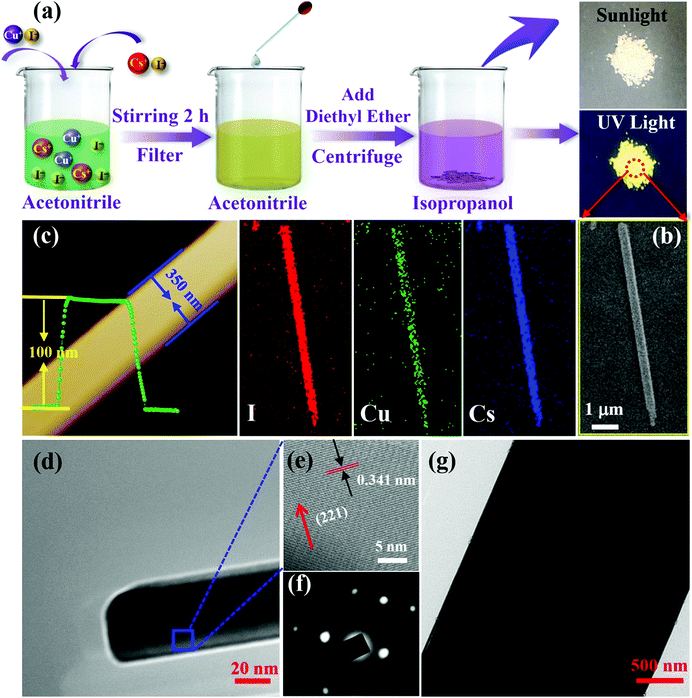 |
| | Fig. 1 (a) Schematic of the processing procedures of the CsCu2I3 NWs. (b) SEM image of an individual NW, and the corresponding EDS mapping showing the uniform distribution of Cs, Cu, and I elements. (c) AFM image of an individual CsCu2I3 wire. TEM images of the CsCu2I3 NWs with a width of (d) 35 nm, and (g) 2 μm. (e) High-resolution TEM image of the CsCu2I3 NW as marked in (d), and the corresponding (f) SAED pattern. | |
The orthorhombic structural characteristics of the produced CsCu2I3 NWs were also tested by X-ray diffraction (XRD). As seen in Fig. 2a, four dominant diffraction peaks at 10.88°, 21.71°, 32.74°, and 44.09° were observed, which can be assigned to the (110), (220), (330), and (242) planes of orthorhombic CsCu2I3 (space group Cmcm, a = 10.505 Å, b = 13.147 Å, c = 6.072 Å, α = β = γ = 90°). No other impurity phases were found, further indicating the good crystallinity of the produced CsCu2I3 NWs. Fig. 2b shows the crystal structure diagram of CsCu2I3, which is composed of a 1D chain structure formed by edge-sharing [CuI4]− dimerized units. Each [CuI4]− tetrahedron is linked by three common edges, forming parallel rod bundles. The Cs+ ions are intercalated between the chains, which are coordinated by eight I− ions in the form of double-capped trigonal prisms. The crystal structures of CsCu2I3 from the top and left view indicate that CsCu2I3 has an anisotropic crystal structure and could easily grow into a 1D linear morphology, which provides the possibility of designing a photodetector by using its anisotropic character. Further, the optical properties of the CsCu2I3 NWs were studied by UV-visible absorption and photoluminescence (PL) spectra. As can be seen from Fig. 2c, a clear absorption edge at around 332.4 nm was observed, and the corresponding Tauc plot of the absorption spectrum (Fig. S3, ESI†) reveals that CsCu2I3 possesses a direct bandgap of 3.73 eV, which is consistent with other articles.36–38 The blue-dotted line displays the PL spectrum of a single CsCu2I3 NW at an excitation wavelength of 330 nm, and an emission peak centered at 542 nm was observed, and the linewidth is 112 nm. It should be mentioned that there is a large Stokes shift of ∼209.6 nm, which implies that the PL mechanism can be explained by excited-state structural reorganization or exciton self-trapping rather than a direct band-to-band transition, and this behavior was frequently observed in low-dimensional metal-halide perovskites.39–41 To better study the optical recombination mechanisms of CsCu2I3, temperature-dependent PL measurements were conducted. As shown in Fig. S4 (ESI†), an obvious thermal quenching behavior of the PL intensity with increasing the temperature can be observed. Fig. S4b (ESI†) shows the relationship between the integrated PL intensity and the reciprocal temperature, and the thermal quenching behavior can be fitted by the following formula:
| |  | (1) |
where
I0 is the emission intensity at 0 K,
A is a proportionality constant, and
kB is the Boltzmann constant. The fitting curve produces a value of 201.7 ± 6.5 meV for the exciton binding energy (
Eb). Further, we measured the PL excitation spectra of CsCu
2I
3 NWs at different emission wavelengths from 470 to 670 nm. As shown in Fig. S5 (ESI
†), the PL excitation spectra show the same properties and shapes, indicating that the PL at 542 nm is caused by the relaxation of the same excited state instead of the defect recombination centers. Considering the anisotropic properties of the CsCu
2I
3 NWs, polarization-dependent PL measurements were therefore performed (one NW with a width of 100 nm was taken as an example) by using a continuous-wave laser (325 nm) as the excitation source, and the schematic diagram of such a measurement configuration is drawn in
Fig. 2d. Note that 0° was defined as the polarization angle parallel to the NWs (the
z-axis labeled in
Fig. 2b).
Fig. 2e shows a color plot showing the variation in the PL intensity
versus the polarization angle. One can see that the emission at around 542 nm shows the maximum intensity at an angle of 0°, and the PL intensity decreases gradually with changing the polarization angle and reaches the minimum at 90° polarization (perpendicular to the wire). The red curve in
Fig. 2f shows the cosine fitting of the PL intensity with a period of 2π, and the PL intensity shows a polarization ratio of ∼1.7
:
1. It should be noted that the polarization ratio herein results from the anisotropic crystal structure and anisotropic morphology simultaneously. An additional observation is that the polarization ratio is inversely proportional to the width of the NWs. As shown in Fig. S6 (ESI
†), a relatively small polarization ratio of ∼1.37 was achieved for the CsCu
2I
3 NW with a width of 6.0 μm, which may be due to the effect of electrostatic dielectric confinement.
28
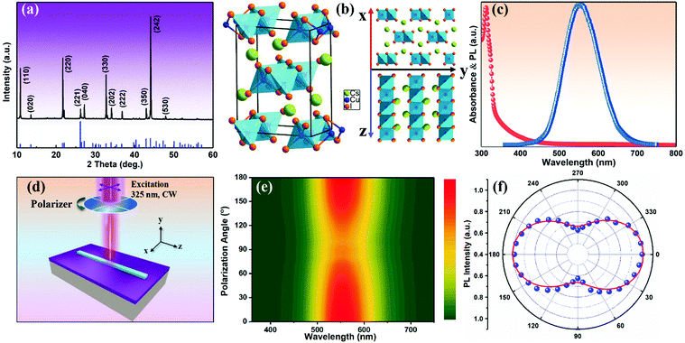 |
| | Fig. 2 (a) Experimental XRD spectrum (top) of the as-grown CsCu2I3 NWs and the standard XRD pattern (bottom) for the orthorhombic CsCu2I3. (b) Crystal structure of CsCu2I3 from side, top, and left views. (c) Steady-state PL and absorption spectra of the CsCu2I3 NWs. (d) Schematic diagram of polarization PL measurements. (e) PL spectra as a function of the incident light polarization. The color represents the emission intensity. (f) Polarization-dependent PL intensity of 1D CsCu2I3 NWs. The data (blue dots) are fitted with a cosine (red) function. | |
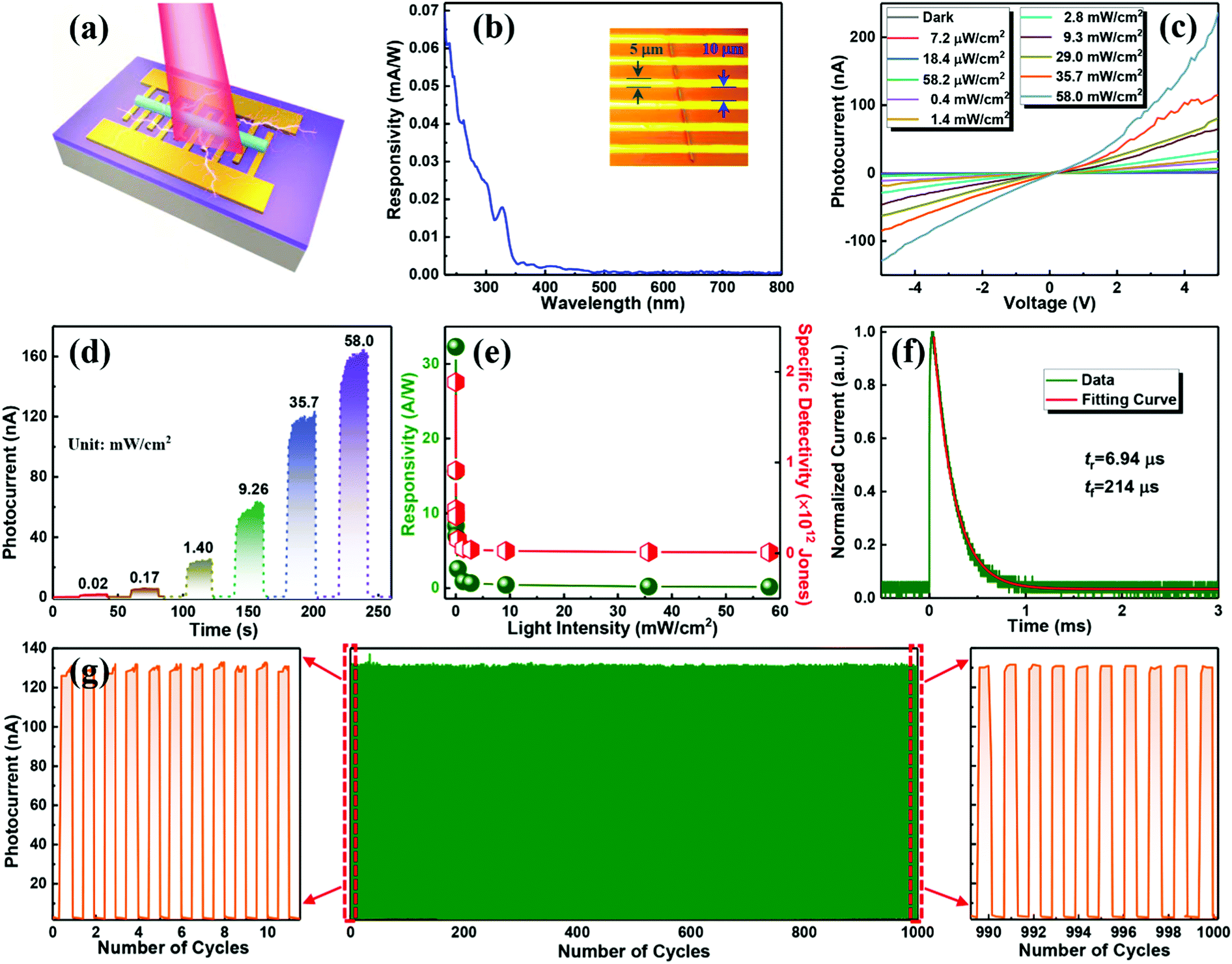
The as-synthesized 1D CsCu2I3 NWs with high crystallinity and strong emission anisotropy suggest their potential as a photoactive material for polarization-sensitive photodetectors. In our case, a metal–semiconductor–metal type photodetector was constructed by transferring a single CsCu2I3 NW to a silicon oxide substrate with Au as the contact electrode, as schematically illustrated in Fig. 3a, and the real device photograph is shown Fig. 3b. Note that the length of the NW used for device fabrication is about 90 μm, and the width is about 600 nm. The energy band alignment of Au/CsCu2I3 was drawn according to the obtained UV-visible absorption spectra together with the UV photoelectron spectroscopy (UPS) data (Fig. S7, ESI†), and a Schottky barrier formed at the hetero-interface. The formation of the Schottky barrier can suppress the leakage current, reduce the dark current, and improve the response speed of the photodetector.
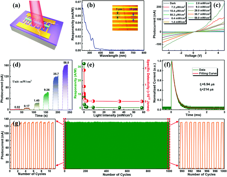 |
| | Fig. 3 (a) Schematic illustration of the photodetector based on an individual CsCu2I3 NW. (b) Spectral response of the photodetector. The inset shows an optical microscope image of the photodetector. (c) I–V and (d) I–t curves of the devices with different light irradiation intensities. (e) Responsivity and specific detectivity of the device versus light irradiation power. (f) Temporal response under 266 nm pulsed laser excitation with a pulse width of 1 ns. (g) One thousand continuous response cycles of the device with a period of 1 s. | |
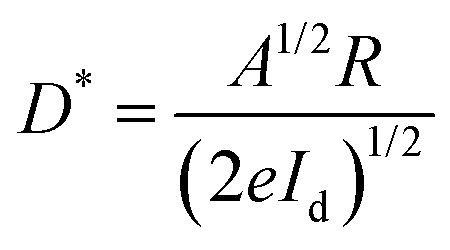
The spectral response in the range of 230–800 nm was firstly tested to achieve the response sensitivity of the photodetector. As seen in Fig. 3b, the device exhibits a photoresponse ranging from 230 to 350 nm, demonstrating the same trend as the absorption spectrum of CsCu2I3 and also suggesting a bandgap excitation process of CsCu2I3.42,43Fig. 3c exhibits the current versus voltage (I–V) characteristics of the photodetector tested in the dark and under light excitation (325 nm) with different irradiation intensities. Owing to the intrinsic low carrier concentration of copper halides, the device displays a rather low dark current of 6.3 × 10⁻¹¹ A under a bias of 5 V, which is beneficial for high detectivity of such device. Following the light illumination, the current increases gradually because the number of photogenerated carriers increases with the absorbed photon flux. In the present case, the I–V curves possessed an asymmetrical behavior, which may be caused by the undesired interface states at the CsCu2I3/Au interface and also the formation of a Schottky barrier. In addition, the curves between photocurrent (IP) and the light intensity can be fitted by the power law of IP = α·Pβ, where α represents a proportionality constant, P is the light intensity, and β is an empirical value that reflects the recombination of photoexcited carriers. As plotted in Fig. S8 (ESI†), fitting the curve in a wide light intensity range gives rise to a value of β = 0.71. The nonunity exponent of the law is due to the complex process of electron–hole generation, trapping, and recombination activity within the CsCu2I3 NW photodetector.44 The current–time (I–t) curves of the photodetector versus varied excitation intensity were also measured, where the pulse bandwidth is 20 s per cycle and the bias voltage is 5 V. As shown in Fig. 3d, the current reversibly switches between high and low conductance with excellent reproducibility and stability, generating a series of tunable on/off ratios. Under a light power of 58.0 mW cm−2, the on/off ratio reaches 2.6 × 10³, which is comparable with the photodetectors based on conventional lead-halide perovskites.45–48 Besides, the photoresponsivity (R) and specific detectivity (D*) are key parameters to quantitatively characterize the photoresponse ability to an optical signal, which can be expressed using the following equations:
| |  | (3) |
in which
Ip represents the photocurrent,
A represents the active area (
A = 54 μm
2), and
Popt is the incident light intensity. Based on the equations, the relationships of
R and
D* with the light intensity at a bias of 5 V are summarized in
Fig. 3e, and the maximum values of
R and
D* for such a photodetector were calculated to be 32.3 A W
−1 and 1.89 × 10
12 Jones (1 Jones = 1 cm Hz
1/2 W
−1), respectively. Note that both
R and
D* decrease with increasing light intensity; this may be due to the enhanced carrier recombination possibility at higher light intensity.
49–51 Besides, we investigated the response time of the CsCu
2I
3 NW-based photodetector by illuminating it with a 266 nm pulsed laser (pulse width 1 ns, 1000 Hz). One can observe that the device could monitor and respond to each pulsed signal (Fig. S9, ESI
†), producing a rise time (
tr) of 6.94 μs defined as the time for the current to increase from 10% to 90% of the peak value, as seen in
Fig. 3f. In addition, by fitting a time-dependent photocurrent curve at the falling edge using an exponential decay curve, the fall time (
tf) of the device is estimated to be ∼214 μs. The fast response speed for such a device is believed to be related to the high crystallinity of the CsCu
2I
3 NWs, which ensures few grain boundaries, a low defect concentration, and a small carrier recombination rate, and therefore facilitates the fast transport of charged photo-generated carriers.
47,52,53 Moreover, the long-term working stability of the CsCu
2I
3 NW-based device was investigated. By using a mechanical chopper with a frequency of 1 Hz to switch the incident light (325 nm, 36 mW cm
−2), the photocurrent signals were obtained by an oscilloscope in real time with a bias voltage of 5 V. As can be seen in
Fig. 3g, the photodetector can maintain its photoresponse ability after 1000 consecutive response cycles, revealing good stability and repeatability.
By virtue of the flexible and deformable structural framework of the 1D NWs, the electrical stability of such a photodetector fabricated on a flexible PET substrate in the bending state was further studied for practical application. As displayed in the insets of Fig. 4a, the device fixed in a vernier caliper was bent at different angles (0°, 60°, 90°, 120°, and 160°) to test its flexibility, and the light intensity was kept at 0.2 mW cm−2 for each cycle (100 s). As shown in Fig. 4a, the current remains almost unchanged under various bending angles, revealing that this flexible photodetector was not influenced by the external bending stress. The excellent electrical stability of the device is also evidenced by the logarithmic I–V curves and I–t period curves under various bending angles, as illustrated in Fig. S10 (ESI†). To further investigate the electrical stability and folding endurance of the flexible photodetector, the logarithmic I–V and I–t curves after different bending cycles with a bending angle of 90° were acquired and put together for comparison. As shown in Fig. 4b and c, the photocurrent, dark current, and photo-switching characteristic of the device were kept very well even after an extreme 1000 bending cycles. The highly flexible photodetector thus opens up opportunities for fundamental research on 1D lead-free perovskites and may greatly expand their application fields especially in portable devices.
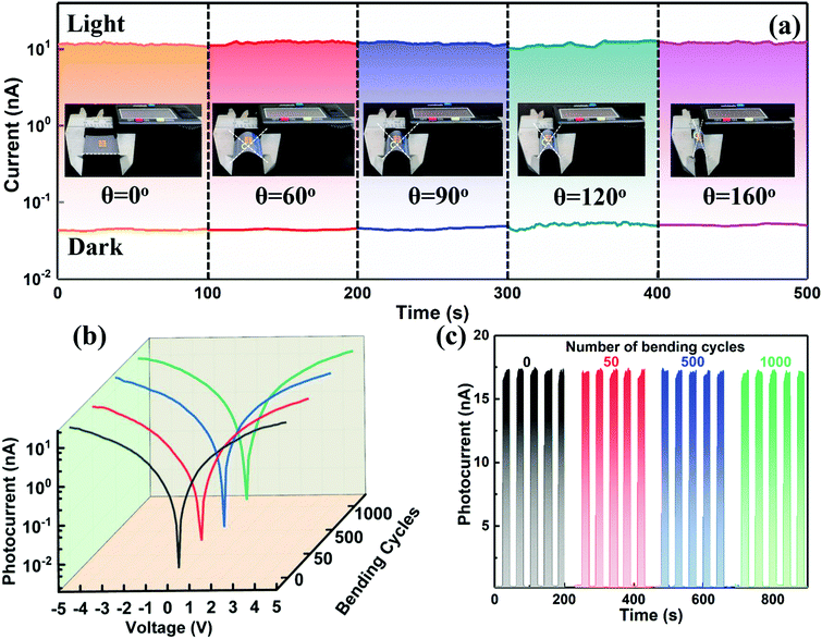 |
| | Fig. 4 (a) Output currents of the device with different bending angles under dark and light illumination with a light intensity of 0.2 mW cm−2 at a bias voltage of 5 V. The insets are the corresponding optical images of the device under five bending states. θ is the bending angle. (b) I–V and (c) I–t curves of the device under different bending cycles. | |
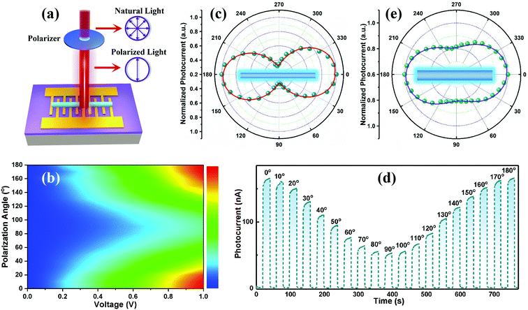
As we all know, in order to realize high-precision detection in complex environments, more information on the light is needed, such as polarimetric information.54–56 The strong anisotropy of 1D CsCu2I3 NWs promotes their applications as a suitable photoactive material for polarization-sensitive photodetectors. In view of this, the incident light was set to pass through a polarizer firstly and then illuminate the NW, as illustrated in Fig. 5a, and the measurements were performed by rotating the polarizer every 10° to change the polarization direction while keeping the light power (58 mW cm−2) constant. Fig. 5b depicts the remarkable anisotropic photoresponse of the photodetector via a 2D colormap within a bias from 0 to 1.0 V. Obviously, upon linearly polarized light excitation, the photocurrent of the device is a strong function of the angle between the polarization of the incident light and the orientation of the NW, as well as the bias voltage. Similar to the polarization-dependent PL spectra, the photocurrent reaches the maximum when the polarization of the light is parallel to the wire (0°) and reaches the minimum when it is perpendicular to it (90°). Then the photocurrent increases with the polarization angle and recovers totally at 180° polarization. The evolution of current at a bias voltage of 1.0 V was further extracted as a function of the polarization angle in polar coordinates, as plotted in Fig. 5c, and a high photocurrent anisotropy ratio of about 3.16 was achieved (defined as the photocurrent tested at a polarization of 0° divided by the photocurrent tested at 90°), which is the maximum value among the perovskite-based polarized photodetectors as far as we know, and also superior to previous studies on 2D materials, such as GeSe (2.16), GeS2 (2.1), GeAs2 (2.0), and so on,54,57–59 as summarized in Table 1. Fig. 5d depicts the corresponding I–t curves of the photodetector as a function of the polarization angle, and an obvious polarization dependence was observed, consistent with the above discussions. Besides, another photodetector with a wider CsCu2I3 wire of 6.0 μm was used for identical measurements. From the polarization angle-dependent curve plotted in Fig. 5e, a relatively smaller photocurrent anisotropy ratio of ∼1.24 was obtained. This trend with smaller width showing higher polarization sensitivity is well consistent with the above polarization-dependent PL results.
 |
| | Fig. 5 (a) Schematic illustration of the polarization-sensitive photodetection based on 1D CsCu2I3 NWs. (b) Anisotropic response in photocurrent under 325 nm light excitation described via a 2D colormap (photocurrent is denoted by the color bar, with voltage as the x-axis and polarization angle as the y-axis). Polarization dependence of the photocurrent for NWs with different widths of (c) 600 nm, and (e) 6.0 μm. (d) Photocurrent response of a 1D CsCu2I3 NW device under incident light with different polarization angles. | |
Table 1 Summary of the performances of the polarization-sensitive photodetectors
| Materials |
Response range (nm) |
Lead-free (yes/no) |
Responsivity (A W−1) |
D* (× 1012 Jones) |
Polarization ratio |
Ref. |
| CH3NH3PbI3 nanowires |
400–800 |
No |
4.95 |
20 |
1.3 |
9
|
| CH3NH3PbCl3 single crystals |
350–450 |
No |
0.0011 |
— |
2.25 |
26
|
| CH3NH3PbI3 nanowires |
400–800 |
No |
1000 |
— |
2.6 |
32
|
| CsPbBr3 nanowires |
400–530 |
No |
0.0115 |
— |
0.78 |
25
|
| CsPbI3 nanowires |
400–800 |
No |
0.745 |
0.035 |
2.68 |
27
|
| (BA)2PbI4 nanowires |
480–600 |
No |
— |
— |
3.62 |
28
|
| CsPbCl3 microcrystals |
300–520 |
No |
0.11 |
0.024 |
3 |
29
|
| Black phosphorus flake |
400–3750 |
Yes |
3.5 × 10⁻⁴ |
— |
3.5 |
4
|
| GeAs2 flake |
400–700 |
Yes |
— |
— |
2 |
57
|
| GeSe flake |
400–950 |
Yes |
— |
— |
2.16 |
58
|
| GeS2 flake |
250–350 |
Yes |
— |
— |
2.1 |
59
|
| ZnO |
400–600 |
Yes |
— |
— |
1.13 |
60
|
| CsCu2I3 nanowires |
250–350 |
Yes |
32.2 |
1.89 |
3.16 |
This work |
Conclusions
In conclusion, high-quality lead-free 1D CsCu2I3 NWs were successfully prepared by an antisolvent engineering approach. The polarization-dependent PL spectra confirm the optical anisotropy of the CsCu2I3 NWs, which results from their intrinsic anisotropy of the asymmetric structure and external morphology anisotropy. Furthermore, we demonstrated a polarization-sensitive photoconductive detector with an individual CsCu2I3 NW as the photoactive material. A record photocurrent anisotropy ratio of ∼3.16 was achieved, which is the maximum value among perovskite-based polarized photodetectors. Moreover, the photodetector exhibits a good detection performance, a large photoresponsivity of ∼32.3 A W−1, a high specific detectivity of 1.89 × 10¹² Jones, and a fast response speed of 6.94/214 μs. In addition, the photodetector fabricated on a flexible substrate demonstrates good flexibility and stability, showing almost no photoresponse degradation after 1000 bending cycles. The results obtained highlight the great potential of such lead-free CsCu2I3 NWs as an attractive candidate to be applied in polarization-sensitive UV photodetectors.
Experimental section
Preparation of CsCu2I3 NWs
0.7 mmol CsI and 1.4 mmol CuI were added to 4 mL anhydrous acetonitrile. The precursor solution was prepared by stirring at 60 °C for 5 h. Then, the precursor solution was naturally cooled down to room temperature. After that, the saturated solution was filtered using a syringe filter of PTFE (0.45 μm). Then, the solution was titrated with anti-solvent (diethyl ether) to precipitate CsCu2I3 wires. By changing the dropping speed of diethyl ether, high-quality 1D CsCu2I3 NWs with different sizes can be obtained.
Fabrication of devices
For polarization-sensitive photodetector fabrication, the as-prepared CsCu2I3 NWs were transferred onto a silicon oxide substrate with Au patterned fingers as the contact electrode, and the Au contact electrode fingers were 5 μm wide and 500 μm long, and the channel spacing was 10 μm. For the flexible photodetector fabrication, a commercially available PET substrate was employed, and other fabrication procedures are the same as above.
Characterization of materials and devices
The morphology of the produced CsCu2I3 wires was studied by field-emission SEM (JEOL-7500F, 15 keV). The element composition was analyzed using an EDS attached to the SEM. XRD (Panalytical X’Pert Pro) was conducted to examine the crystallinity of the products. AFM (Dimension Icon, Bruker) was used to study the morphology and height profiles of the CsCu2I3 NWs. The PL spectra were studied using a spectrofluorometer (Horiba; Fluorolog-3). A closed-cycle helium cryostat (Jannis; CCS-110) was used to carry out the PL measurements at different temperatures. The absorption spectra were measured using a Shimadzu UV-3150 spectrophotometer. UPS was conducted to study the energy band properties, and the UPS radiation was generated by a He-gas discharge lamp (He I = 21.22 eV). The optoelectrical and electrical measurements of the photodetectors were conducted by using a testing system that includes an oscilloscope (Tektronix, DPO2012B), an optical chopper (SRS, SR540), a digital SourceMeter (Keithley 2636B), a monochromator, and light sources in ambient air. A Xe lamp (Gloria-X150A, Zolix) equipped with a monochromator (Omni-λ300, Zolix) was used to generate the monochromatic light to conduct the spectral response measurements.
Conflicts of interest
There are no conflicts to declare.
Acknowledgements
This work was supported by the National Natural Science Foundation of China (No. 11774318, 61935009, and 11604302), the Key Scientific Research Projects of Higher Education in Henan Province (18A140007), and the Support Program for Scientific and Technological Innovation Talents of Higher Education in Henan Province (19HASTIT017).
Notes and references
- M. Long, A. Gao, P. Wang, H. Xia, C. Ott, C. Pan, Y. Fu, E. Liu, X. Chen and W. Lu, Sci. Adv., 2017, 3, 1700589 CrossRef PubMed
 .
.
- J. Wang, M. S. Gudiksen, X. Duan, Y. Cui and C. M. Lieber, Science, 2001, 293, 1455 CrossRef CAS PubMed .
- F. Xia, H. Wang and Y. Jia, Nat. Commun., 2014, 5, 4458 CrossRef CAS PubMed .
- H. Yuan, X. Liu, F. Afshinmanesh, W. Li, G. Xu, J. Sun, B. Lian, A. G. Curto, G. Ye and Y. Hikita, Nat. Nanotechnol., 2015, 10, 707 CrossRef CAS PubMed .
- X. W. Wang, A. M. Jones, K. L. Seyler, V. Tran, Y. C. Jia, H. Zhao, H. Wang, L. Yang, X. D. Xu and F. N. Xia, Nat. Nanotechnol., 2015, 10, 517 CrossRef CAS PubMed .
- L. F. Li, S. Z. Lu, J. B. Pan, Z. H. Qin, Y. Q. Wang, Y. L. Wang, G. Y. Cao, S. X. Du and H. J. Gao, Adv. Mater., 2014, 26, 4820 CrossRef CAS PubMed .
- C. Chao, D. C. Bobela, Y. Yang, S. C. Lu, K. Zeng, C. Ge, B. Yang, L. Gao, Y. Zhao, M. C. Beard and J. Tang, Front. Optoelectron., 2017, 10, 18 CrossRef .
- H. Song, T. Li, J. Zhang, Y. Zhou, J. Luo, C. Chen, B. Yang, C. Ge, Y. Wu and J. Tang, Adv. Mater., 2017, 29, 1700441 CrossRef PubMed .
- L. Gao, K. Zeng, J. Guo, C. Ge, J. Du, Y. Zhao, C. Chen, H. Deng, Y. He, H. Song, G. Niu and J. Tang, Nano Lett., 2016, 16, 7446 CrossRef CAS PubMed .
- X. He, W. Gao, L. Xie, B. Li, Q. Zhang, S. Lei, J. M. Robinson, E. H. Hároz, S. K. Doorn, W. Wang, R. Vajtai, P. M. Ajayan, W. W. Adams, R. H. Hauge and J. Kono, Nat. Nanotechnol., 2016, 11, 633 CrossRef CAS PubMed .
- A. Singh, X. Y. Li, V. Protasenko, G. Galantai, M. Kuno, H. Xing and D. Jena, Nano Lett., 2007, 7, 2999 CrossRef CAS PubMed .
- Y. Wang, X. M. Li, J. Z. Song, L. Xiao, H. B. Zeng and H. D. Sun, Adv. Mater., 2015, 27, 7101 CrossRef CAS PubMed .
- Y. Li, Z. Shi, L. Lei, S. Li, D. Yang, D. Wu, T. Xu, Y. Tian, Y. Lu, Y. Wang, L. Zhang, X. Li, Y. Zhang, G. Du and C. Shan, Adv. Mater. Interfaces, 2019, 6, 1900188 CrossRef .
- G. C. Xing, N. Mathews, S. Y. Sun, S. S. Lim, Y. M. Lam, M. Grätzel, S. Mhaisalkar and T. C. Sum, Science, 2013, 342, 344 CrossRef CAS PubMed .
- J. Chen, L. Gan, F. Zhuge, H. Li, J. Song, H. Zeng and T. Zhai, Angew. Chem., Int. Ed., 2017, 56, 2390 CrossRef CAS PubMed .
- J. Burschka, N. Pellet, S. J. Moon, R. Humphry-Baker, P. Gao, M. K. Nazeeruddin and M. Grätzel, Nature, 2013, 499, 316 CrossRef CAS PubMed .
- Y. Zhang, J. Du, X. Wu, G. Zhang, Y. Chu, D. Liu, Y. Zhao, Z. Liang and J. Huang, ACS Appl. Mater. Interfaces, 2015, 7, 21634 CrossRef CAS PubMed .
- M. Y. Leng, Z. W. Chen, Y. Yang, Z. Li, K. Zeng, K. H. Li, G. D. Niu, Y. He, Q. C. Zhou and J. Tang, Angew. Chem., Int. Ed., 2016, 55, 15012 CrossRef CAS PubMed .
- Z. Shi, Y. Li, Y. Zhang, Y. Chen, X. Li, D. Wu, T. Xu, C. Shan and G. Du, Nano Lett., 2017, 17, 313 CrossRef CAS PubMed .
- Z. Gu, Z. Huang, C. Li, M. Li and Y. Song, Sci. Adv., 2018, 4, eaat2390 CrossRef PubMed .
- Y. Zhang, W. X. Xu, X. J. Xu, J. Cai, W. Yang and X. S. Fang, J. Phys. Chem. Lett., 2019, 10, 836 CrossRef CAS PubMed .
- X. Hu, H. Zhou, Z. Y. Jiang, X. Wang, S. P. Yuan, J. Y. Lan, Y. P. Fu, X. H. Zhang, W. B. Zheng, X. X. Wang, X. L. Zhu, L. Liao, G. Z. Xu, S. Jin and A. L. Pan, ACS Nano, 2017, 11, 9869 CrossRef CAS PubMed .
- X. Gong, M. Tong, Y. Xia, W. Cai, J. Moon, Y. Cao, G. Yu, C. Shieh, B. Nilsson and A. J. Heeger, Science, 2009, 325, 1665 CrossRef CAS PubMed .
- Z. Shi, S. Li, Y. Li, H. Ji, X. Li, D. Wu, T. Xu, Y. S. Chen, Y. Tian, Y. Zhang, C. Shan and G. Du, ACS Nano, 2018, 12, 1462 CrossRef CAS PubMed .
- Y. Gao, L. Zhao, Q. Shang, Y. Zhong, Z. Liu, J. Chen, Z. Zhang, J. Shi, W. Du, Y. Zhang, S. Chen, P. Gao, X. Liu, X. Wang and Q. Zhang, Adv. Mater., 2018, 30, 1801805 CrossRef PubMed .
- J. X. Ding, X. H. Cheng, L. Jing, T. L. Zhou, Y. Zhao and S. J. Du, ACS Appl. Mater. Interfaces, 2017, 10, 845 CrossRef PubMed .
- Y. Zhou, J. Luo, Y. Zhao, C. Ge, C. Wang, L. Gao, C. Zhang, M. Hu, G. Niu and J. Tang, Adv. Opt. Mater., 2018, 6, 1800679 CrossRef .
- D. Ghoshal, T. Wang, H. Z. Tsai, S. W. Chang, M. Crommie, N. Koratkar and S. F. Shi, Adv. Opt. Mater., 2019, 7, 1900039 CrossRef .
- X. Z. Hu, X. Y. Wang, S. D. Zhuang and J. Q. Xu, CrystEngComm, 2020, 22, 178 RSC .
- X. Cheng, J. Q. Ma, Y. X. Zhou, C. Fang, J. Wang, J. Z. Li, X. L. Wen and D. H. Li, J. Phys.: Photonics, 2020, 2, 014008 Search PubMed .
- Y. B. Li, T. Yang, Z. Y. Xu, X. T. Liu, X. Y. Huang, S. G. Han, Y. Liu, M. F. Li, J. H. Luo and Z. H. Sun, Angew. Chem., Int. Ed., 2020, 59, 3429 CrossRef CAS PubMed .
- J. Feng, X. Yan, Y. Liu, H. Gao, Y. Wu, B. Su and L. Jiang, Adv. Mater., 2017, 29, 1605993 CrossRef PubMed .
- Y. Li, Z. Shi, W. Q. Liang, L. Wang, S. Li, F. Zhang, Z. Ma, Y. Wang, Y. Tian, D. Wu, X. Li, Y. Zhang, C. Shan and X. Fang, Mater. Horiz., 2020, 7, 530 RSC .
- N. J. Jeon, J. H. Noh, Y. C. Kim, W. S. Yang, S. Ryu and S. Seok, Nat. Mater., 2014, 13, 897 CrossRef CAS PubMed .
- Z. Z. Ma, Z. Shi, L. Wang, F. Zhang, D. Wu, D. W. Yang, X. Chen, Y. Zhang, C. X. Shan and X. J. Li, Nanoscale, 2020, 12, 3637 RSC .
- T. Jun, T. Handa, K. Sim, S. Limura, M. Sasase, J. Kim, Y. Kanemitsu and H. Hosono, APL Mater., 2019, 7, 111113 CrossRef .
- M. Du, ACS Energy Lett., 2020, 5, 464 CrossRef CAS .
- P. Vashishtha, G. Nutan, B. Griffith, Y. Fang, D. Giovanni, M. Jagadeeswararao, T. Sum, N. Mathews, S. Mhaisalkar, J. Hanna and T. White, Chem. Mater., 2019, 31, 9003 CrossRef CAS .
- T. Jun, K. Sim, S. Iimura, M. Sasase, H. Kamioka, J. Kim and H. Hosono, Adv. Mater., 2018, 30, 1804547 CrossRef PubMed .
- C. Zhou, Y. Tian, M. Wang, A. Rose, T. Besara, N. K. Doyle, Z. Yuan, J. C. Wang, R. Clark, Y. Y. Hu, T. Siegrist, S. C. Lin and B. W. Ma, Angew. Chem., Int. Ed., 2017, 56, 9018 CrossRef CAS PubMed .
- Z. Yuan, C. Zhou, Y. Tian, Y. Shu, J. Messier, J. C. Wang, L. J. V. D. Burgt, K. Kountouriotis, Y. Xin, E. Holt, K. Schanze, R. Clark, T. Siegrist and B. W. Ma, Nat. Commun., 2017, 8, 14051 CrossRef CAS PubMed .
- C. Ji, P. Wang, Z. Wu, Z. Sun, L. Li, J. Zhang, W. Hu, M. Hong and J. Luo, Adv. Funct. Mater., 2018, 28, 1705467 CrossRef .
- Y. Liu, Z. Yang, D. Cui, X. Ren, J. Sun, X. Liu, J. Zhang, Q. Wei, H. Fan, F. Yu, X. Zhang, C. Zhao and S. Z. Liu, Adv. Mater., 2015, 27, 5176 CrossRef CAS PubMed .
- Y. Li, Z. Shi, X. Li and C. Shan, Chin. Phys. B, 2019, 28, 017803 CrossRef CAS .
- J. R. Zhang, Q. Wang, X. S. Zhang, J. X. Jiang, Z. F. Gao, Z. W. Jin and S. Z. Liu, RSC Adv., 2017, 7, 36722 RSC .
- J. Chen, Y. Fu, L. Samad, L. Dang, Y. Zhao, S. Shen, L. Guo and S. Jin, Nano Lett., 2017, 17, 460 CrossRef CAS PubMed .
- S. Li, Y. Li, Z. Shi, L. Lei, H. Ji, D. Wu, T. Xu, X. Li and G. Du, Sol. Energy Mater. Sol. Cells, 2019, 191, 275 CrossRef CAS .
- X. M. Li, D. J. Yu, F. Cao, Y. Gu, Y. Wei, Y. Wu, J. Z. Song and H. B. Zeng, Adv. Funct. Mater., 2016, 26, 5903 CrossRef CAS .
- G. Konstantatos, I. Howard, A. Fischer, S. Hoogland, J. Clifford, E. Klem, L. Levina and E. H. Sargent, Nature, 2006, 442, 180 CrossRef CAS PubMed .
- W. Y. Kong, G. A. Wu, K. Y. Wang, T. F. Zhang, Y. F. Zou, D. D. Wang and L. B. Luo, Adv. Mater., 2016, 28, 10725 CrossRef CAS PubMed .
- L. H. Zeng, S. H. Lin, Z. J. Li, Z. X. Zhang, T. F. Zhang, C. Xie, C. H. Mak, Y. Chai, S. P. Lau, L. B. Luo and Y. H. Tsang, Adv. Funct. Mater., 2018, 28, 1705970 CrossRef .
- L. Q. Pang, Y. Yao, Q. Wang, X. S. Zhang, Z. W. Jin and S. Z. Liu, Part. Part. Syst. Charact., 2018, 35, 1700363 CrossRef .
- Y. Li, Z. Shi, L. Z. Lei, Z. Ma, F. Zhang, S. Li, D. Wu, T. Xu, X. Li, C. Shan and G. Du, ACS Photonics, 2018, 5, 2524 CrossRef CAS .
- C. Jia, X. W. Huang, D. Wu, Y. Z. Tian, J. W. Guo, Z. H. Zhao, Z. F. Shi, Y. T. Tian, J. S. Jie and X. J. Li, Nanoscale, 2020, 12, 4435 RSC .
- Z. Q. Zhou, M. S. Long, L. F. Pan, X. T. Wang, M. Z. Zhong, M. Blei, J. Wang, J. Z. Fang, S. Tongay, W. D. Hu, J. B. Li and Z. M. Wei, ACS Nano, 2018, 12, 12416 CrossRef CAS PubMed .
- Y. Yan, W. Q. Xiong, S. S. Li, K. Zhao, X. T. Wang, J. Su, X. H. Song, X. P. Li, S. Zhang, H. Yang, X. F. Liu, L. Jiang, T. Y. Zhai, C. X. Xia, J. B. Li and Z. M. Wei, Adv. Opt. Mater., 2019, 7, 1900622 CrossRef CAS .
- L. Li, P. L. Gong, D. P. Sheng, S. Wang, W. K. Wang, X. D. Zhu, X. Q. Shi, F. K. Wang, W. Han, S. J. Yang, K. L. Liu, H. Q. Li and T. Y. Zhai, Adv. Mater., 2018, 30, 1804541 CrossRef PubMed .
- X. T. Wang, Y. T. Li, L. Huang, X. W. Jiang, L. Jiang, H. L. Dong, Z. M. Wei, J. B. Li and W. P. Hu, J. Am. Chem. Soc., 2017, 139, 14976 CrossRef CAS PubMed .
- Y. Yang, S. C. Liu, X. Wang, Z. B. Li, Y. Zhang, G. M. Zhang, D. J. Xue and J. S. Hu, Adv. Funct. Mater., 2019, 29, 1900411 CrossRef .
- Z. M. Liao, J. Xu, J. M. Zhang and D. P. Yu, Chin. Phys. Lett., 2008, 25, 2622 CrossRef CAS .
Footnote |
| † Electronic supplementary information (ESI) available: SEM images of the 1D CsCu2I3 nanowires with different widths, EDS spectra of the CsCu2I3 nanowires, calculation of the optical bandgap of the CsCu2I3 nanowires using the Tauc method, temperature-dependent PL spectra and the calculation of the exciton binding energy, PLE spectra of the CsCu2I3 nanowires measured at different emission wavelengths from 470 to 670 nm, PL intensity as a function of the excitation polarization in a polar plot, UPS data and the energy band profile of the Au/CsCu2I3 contact, dependence of photocurrent on the incident light power density of the photodetector, time-resolved photoresponse curves of the device excited by a 266 nm pulsed laser for ten cycles, I–V and I–t curves of the device measured at different bending angles. See DOI: 10.1039/d0mh00250j |
|
| This journal is © The Royal Society of Chemistry 2020 |
Click here to see how this site uses Cookies. View our privacy policy here. 
 *a,
Lintao
Wang
a,
Yancheng
Chen
a,
Wenqing
Liang
a,
Di
Wu
*a,
Lintao
Wang
a,
Yancheng
Chen
a,
Wenqing
Liang
a,
Di
Wu