
Soluble poly(4-fluorostyrene): a high-performance dielectric electret for organic transistors and memories†
Yuanwei
Zhu
a,
Yongkang
Fan
a,
Shengtao
Li
*a,
Peng
Wei
a,
Dongfan
Li
a,
Bo
Liu
*b,
Dongmei
Cui
 b,
Zhicheng
Zhang
c,
Guochang
Li
d,
Yongjie
Nie
e and
Guanghao
Lu
*a
b,
Zhicheng
Zhang
c,
Guochang
Li
d,
Yongjie
Nie
e and
Guanghao
Lu
*a
aFrontier Institute of Science and Technology and State Key Laboratory of Electrical Insulation and Power Equipment, Xi'an Jiaotong University, Xi'an, 710054, China. E-mail: guanghao.lu@xjtu.edu.cn; sli@xjtu.edu.cn
bState Key Laboratory of Polymer Physics and Chemistry, Changchun Institute of Applied Chemistry, Chinese Academy of Science, Changchun, 130022, China. E-mail: liubo@ciac.ac.cn
cSchool of Science, Xi'an Jiaotong University, Xi'an, 710054, China
dQingdao University of Science and Technology, Qingdao, 266042, China
eElectric Power Research Institute, Yunnan Power Grid Co., Ltd, Kunming, 650217, China
First published on 17th April 2020
Abstract
Electrets, referring to an insulating dielectric material carrying quasi-permanent neat charges, are attracting interest for their potential wide applications in electronic devices, filtration fabrics and biological/medical sterilization. Here we report a high-performance, optical transparent and solution-processible polymer electret, atactic poly(4-fluorostyrene) (FPS), synthesized by radical polymerization. The deep bulk traps of FPS could stably accommodate charges, and the hydrophobicity of this material prevents moisture invasion in ambient environments, both of which contribute to the high environmental-stability. Subsequently, the solution processed FPS film with a high sheet charge density of 6.8 × 1012 cm−2, high dielectric strength, good thermal stability and decreased leakage current is introduced as a gate dielectric for organic field effect transistors (OFETs) and non-volatile memories. Using FPS-coated SiO2 as the gate dielectric and 2,7-didodecyl[1]benzothieno[3,2-b][1]benzothiophene (C12-BTBT) as the semiconductor, OFETs can work with a high mobility of 11.2 cm2 V−1 s−1 and on/off ratio of 107, along with a large memory window of 108 V, and enhanced memory stability over one month during direct exposure to ambient air. Finally, we use a conjugated polymer blended with FPS to show the general improvement of OFET performance by our FPS electret.
New conceptsA polymer electret carrying neat charges serves as a floating gate can manipulate organic field effect transistors (OFETs) performance, which enables improved application potential for OFET-based non-volatile memories, sensors, and integrated circuits. However, such charges are usually not stably trapped in an electret, threatening the long-term operation of the electronic device. Herein, we introduce a new soluble polymer, atactic poly(4-fluorostyrene) (FPS). The electron and hole trap densities of FPS are increased by 29.6% and 9.6%, respectively, along with an increased trap energy over 0.1 eV, as compared to the model dielectric polystyrene. As a result, the charge storage capability reaching 6.8 × 1012 cm−2, and charge storage stability over one month in ambient air, of FPS, are superior to state-of-the-art polymer electrets. With our FPS gate dielectric, general improvements in operation performance and memory stability of OFETs are achieved with both small molecule and polymer semiconductors, showing the wide-potential of FPS. |
Introduction
Compared with metals and semiconductors, an insulator is electrically resistant. This feature implies that charges trapped in an insulator do not easily leak away, and such a dielectric insulator with quasi-permanent neat charges is generally called an electret. Electrets are widely used in electronic devices,1–3 filtration fabrics,4,5 electrostatic printing6 and biological/medical sterilizations.7,8 However, due to ambient humidity, the charge population in an electret typically decays quickly during direct exposure to air. Currently, the community is looking for electret materials with higher charge trapping density and longer retention time.9 On the other hand, organic field effect transistors (OFETs) are attracting wide attention as the next generation electronic device, owing to their particular characteristics of low cost, large area solution processability and mechanical flexibility.10–13 Practical applications require OFETs with high mobility, large on/off ratio, appropriate threshold voltage and good stability. The performance optimization of an OFET can be achieved by constructing a dielectric electret (floating gate) between a semiconductor and gate electrode.14–17 With the additional electric field generated by the floating gate, OFET performance such as field-effect mobility, on/off ratio, and sub-threshold swing can be manipulated, enabling great application potential for OFET-based non-volatile memories, sensors, and integrated circuits.1,18–20In non-volatile memories containing an electret, a sufficiently large shift of transfer characteristic manipulated by the gate voltage is required.21–23 As OFET memory has drawn significant attention recently, optimization investigations of dielectric layers have been carried out, which particularly focus on the design and synthesis of dielectric polymers to improve charge storage properties.24–28 For example, functional groups were grafted onto polystyrene (PS) to achieve higher charge storage/trapping capability,2,3 and the charge density of an electret was enhanced to 5.7 × 1012 cm−2 for poly(α-methylstyrene) (PαMS).29 Another strategy to enhance charge storage capability is the design of fluorinated polymers; due to the strong electronegativity of F atoms.22,30–37 Poly(pentafluorostyrene) (PFS),38 poly[bis-(4-aminophenyl)fluorene-hexafluoroiso propylidene diphthalimide] (PI(BAPF-6FDA)),39 and poly(3-trifluoromethylstyrene) (P3TFMS)40 were proposed to fabricate OFETs, and for instance, the trapped charge density was enlarged to 5.3 × 1012 cm−2 with an enhanced memory window of 77 V in a PI(BAPF-6FDA)/pentacene structure.39 Some of the representative electret polymers and their OFET performances are summarized in Table S1 in the ESI.† It is demonstrated that for these previously reported dielectric electrets, the field effect mobility and on/off ratio of the OFET are not improved with the increased memory window. For instance, the mobility of a PαMS/pentacene OFET is 0.35 cm2 V−1 s−1 with an on/off ratio of 105.3 Other reported device characteristics are still not satisfactory, which greatly limits the further development and practical operation of OFET memories. Therefore, improving OFET performance along with enhanced memory characteristics becomes a challenging issue.
For non-volatile characteristics of electret OFETs, the long-term stability of the charged electret is the key factor. However, according to Table S2 (ESI†), the intensity of most electrets generated in the dielectric polymers of OFETs, quickly decays within minutes to hours.41–44 Also, more than 70% of the reported data were obtained in a laboratory nitrogen environment without moisture,23,45,46 which can hardly be representative of ambient conditions.24 For example, the mobility of a pentacene OFET could experience an obvious loss from 0.62 cm2 V−1 s−1 to 0.12 cm2 V−1 s−1 in ambient conditions.26 Therefore, stability, memory window, and OFET performance need to be simultaneously achieved, as shown by our in-depth understanding of the contributions of gate dielectrics in transistors and memories.
In this work, a new polymeric material, poly(4-fluorostyrene) (FPS) is synthesized and applied as the gate dielectric in OFETs. Differential scanning calorimetry (DSC), thermogravimetric analysis (TGA), UV-visible absorption, water contact angle, permittivity, dielectric loss and dielectric breakdown of FPS are systematically investigated. FPS is compared with the widely-used model dielectric material, polystyrene. Two organic semiconductors, 2,7-didodecyl[1]benzothieno[3,2-b][1]benzothiophene (C12-BTBT) and poly[4-(4,4-dihexadecyl-4H-cyclopenta[1,2-b:5,4-b′]dithophen-2-yl)-alt-[1,2,5]-thiadiazolo [3,4-c]pyridine] (PCDTPT), are applied to form a C12-BTBT/FPS bilayer and PCDTPT/PS blend, respectively, to demonstrate the general application potential of FPS for high performance OFETs with long-term memory stability.
Results and discussion
FPS was prepared through radical polymerization as shown in Fig. 1a, the details of the synthesis are provided in the Synthesis and device fabrication section of the Experimental. Fig. S1 (ESI†) shows the 1H NMR spectrum of FPS, and Fig. S2 (ESI†) shows Mw = 1600 kDa, and PDI = 1.25. Fig. 1b shows the water contact angle results of PS and FPS films respectively, which shows that PS has a contact angle of 86.6°, while that of FPS is 97.3°. The solution spin coated PS and FPS films are both amorphous with a flat surface. Consequently, the difference in terms of contact angle is ascribed to the chemical structure between PS and FPS. As a well-known phenomenon, fluorinated polymers generally feature lower surface energy, as compared with non-fluorinated ones.47 This leads to a hydrophobic surface, preventing moisture from invading. Fig. 1c shows the TGA profile of PS and FPS, from which the thermal decomposition temperatures of PS and FPS are extracted as 391 °C and 396 °C, respectively, demonstrating a 5 °C increase from PS to FPS. This improved thermal stability is due to the fluorinated benzene ring. The heat scanning of the DSC result (Fig. 1d) shows that the glass transition temperatures (Tg) of PS and FPS are 110 °C and 118.0 °C, respectively. For dielectric materials in electronic applications, a higher Tg refers to higher operational stability. As compared with PS, FPS has a higher polarity as a result of the grafted F atom, contributing to the higher Tg. The UV-vis absorption spectra (Fig. 1e) demonstrates that FPS is highly transparent in the visible wavelength range, indicating the application potential in transparent electronics. The absorption peak of FPS is 192 nm, which is closer to the vacuum ultraviolet region as compared with that of PS (196 nm).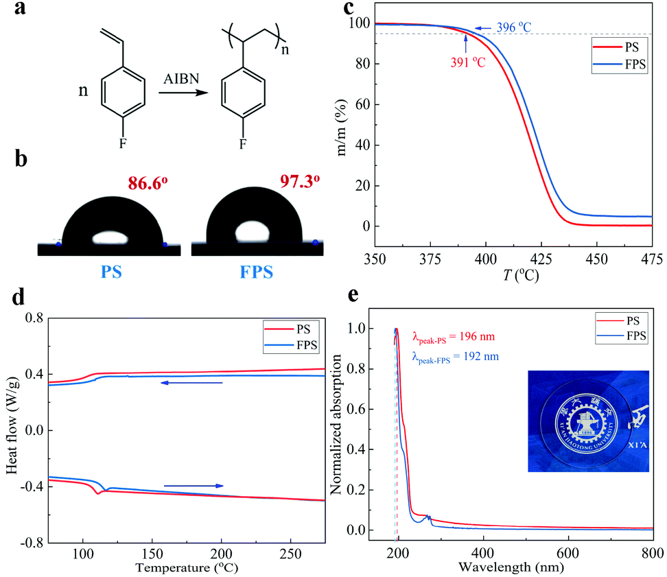 | ||
| Fig. 1 Chemical and physical characterization of FPS. (a) Synthesis of poly(4-fluorostyrene). (b) Water contact angles of PS (θ = 86.6°) and FPS (θ = 97.3°) films, respectively. (c) TGA profiles of PS and FPS. (d) DSC of PS and FPS. The arrows show the temperature scanning direction. (e) Normalized UV-vis absorption spectra of PS and FPS. Inset shows a photo of FPS coated glass (the circle shape in the photo) showing the high optical transparency of FPS. | ||
Accurate characterization of the charge storage capability of a gate dielectric is important in manipulating OFET performance. However, current methods are either qualitative or based on the equation16,21,48
The ISPD applies a high voltage needle and a grid electrode to emit charges (positive or negative) on to the upper surface of a dielectric film,49–51 as shown in Fig. 2a. The applied voltage is sufficiently high (which is at the kV level) so that multiple charges can deposit from the film surface, and migrate into the bulk of the sample, filling surface and bulk traps. For clarity, in Fig. 2a we demonstrate the strong electric field surrounding the FPS electret. The FPS electret (in the rectangle area highlighted with a blue boarder) held by tweezers is moved towards the paper pieces and the paper pieces are incrementally attracted by the electret (left photo). Afterwards, the FPS electret is moved upwards, carrying the paper pieces with it as a result of electrostatic interaction (right photo). These trapped charges generate a built-in electric field which establishes a surface potential that can be measured by a non-contact potential probe. After the charge injection, the back surface of the dielectric film is grounded, and thus the trapped charges can slowly detrap, leading to a decreased surface potential. Therefore, the whole detrapping process can be described by analyzing the obtained surface potential decay. Afterwards the trap density and trap energy (also known as trap depth, in eV) are thus obtained by further data processing.50 We apply both positive and negative charging processes in analyzing the charge storage capability of both PS and FPS dielectric polymers (Fig. 2b).
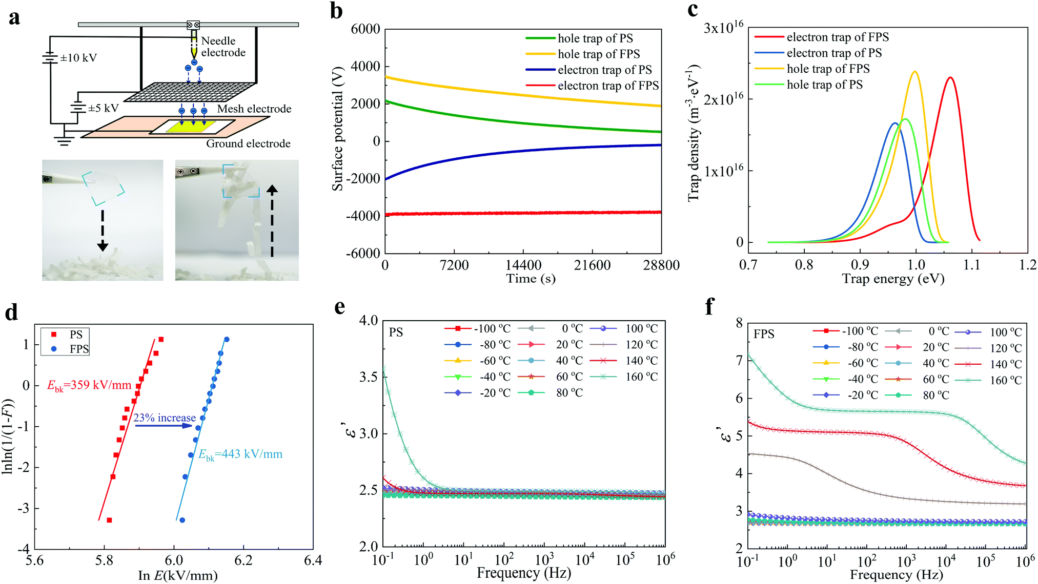 | ||
| Fig. 2 Dielectric and charge storage characteristics of FPS. (a) Scheme of our ISPD test system for charge trap characterization. The bottom image shows the photos of the FPS electret inducing electrostatic fields in the space surrounding the electret. The FPS electret (in the rectangle area highlighted with a blue boarder) held by tweezers is moving downwards to paper pieces and the paper pieces are incrementally attracted by the electret (left photo). Afterwards, the FPS electret is moved upwards, carrying the paper pieces with it as a result of electrostatic interactions (right photo). The dashed arrows show the moving direction of the FPS electret. (b) The ISPD results of PS and FPS for both electrons and holes. (c) The distribution of electron and hole traps in PS and FPS. (d) DC dielectric breakdown strength of PS and FPS with statistical data from 15 samples. (e and f) The dependence of dielectric permittivity of PS (e) and FPS (f) on the frequency, at temperatures of −100 to 160 °C. | ||
In Fig. 2b, the initial hole potential of FPS is larger than that of PS, reaching 3500 V, which indicates more hole traps per unit volume. For electrons, FPS also shows a higher initial surface potential. It is noticed that the decay rates of holes for PS and FPS are similar, which means the hole trap energies of the two materials are almost the same. However, for electrons, PS experiences a rapid decay, reaching 0 V at 28![[thin space (1/6-em)]](https://www.rsc.org/images/entities/char_2009.gif) 800 s, while that of FPS rarely changes during the testing process. Thus, electrons are more firmly trapped in FPS, owning to the increased trap energy.
800 s, while that of FPS rarely changes during the testing process. Thus, electrons are more firmly trapped in FPS, owning to the increased trap energy.
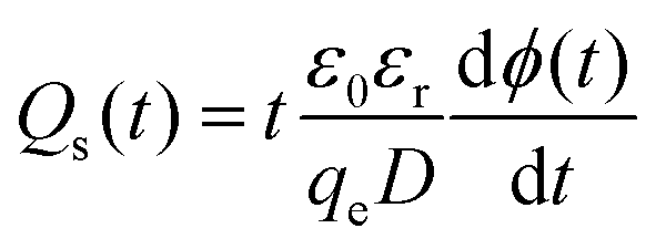
In order to quantitatively analyze the charge storage capability of PS and FPS, an improved Simmon's theory is utilized to analyze the charge trap information from the isothermal current decay of semiconductors and insulators.52 The charge trap density and trap energy can be expressed as,49,53
| ET = kBTln(νATEt) |
where ET is the trap energy; kB is the Boltzmann constant; T is temperature; νATE is the attempt-to-escape frequency of charges, which can be expressed as νATE = (kBT)3/dh3ν2, where h is the Planck’s constant, the value of d is 6, and ν is the vibration frequency around the defects at the orthogonal plane flaw in the direction of motion; t is time; Qs is trap density; ε0 is the vacuum permittivity; εr is the relative permittivity of the dielectric, which is obtained from the experiments in Fig. 2e and f; D is the sample thickness; ϕ is the surface potential of the charged material.
Based on these equations, the distributions of trap energy and trap density in PS and FPS are obtained, as demonstrated in Fig. 2c. The peak of hole trap energy of PS is around 0.98 eV, while that of FPS is 1.00 eV. Therefore in FPS, the injected positive charges are more firmly trapped. Generally in dielectric materials, deep traps with trap energy around 0.8–1.0 eV commonly exist,54–57 which are considered to dominate the electrical insulating performance and charge storage capability of the material.57,58 A 0.02 eV increase is sufficiently large to create a dramatically prolonged storage time of trapped charges (retention time in OFET),57 leading to the improved stability of the electret in OFETs. More obviously, the trap energy of the electron is tremendously increased from 0.96 eV in PS to 1.06 eV in FPS. This increase is considered to be generated by the grafted F atom, which results in the generation of deeper electron traps as the F atom has a higher electronegativity than a H atom. Actually, only one peak of 0.96 eV is identified for PS, thus the deeper traps of 1.06 eV are generated by the F atom.
In terms of trap density, the integral area of each curve in Fig. 2c represents the total trap amount. It is observed that the trap density of PS is much lower than that of FPS. In other words, the fluorinated polymer introduces more traps,59,60 for both electrons and holes. In detail, the hole trap amount is increased by 9.6%, from 1.23 × 10¹⁵ m−3 in PS to 1.35 × 10¹⁵ m−3 in FPS; while electron trap density is increased by 29.6% from 1.35 × 10¹⁵ m−3 in PS to 1.75 × 10¹⁵ m−3 in FPS. Thus, the fluorinated polymer introduces more electron traps than hole traps.
In recent years, the relation between deep traps and dielectric breakdown performance was discovered.57,61 Deeper traps can suppress charge acceleration under extreme high voltage conditions, resulting in improved breakdown strength.55Fig. 2d shows the DC breakdown results of PS and FPS, and the results are demonstrated with Weibull distributions,62 in which E is the breakdown strength, and F is the Ross distribution function of the possibility for breakdown. The results demonstrate that the average DC breakdown strength of FPS reaches 443 kV mm−1, showing an improvement over 23% as compared with PS. A nano composite insulating material was recently proposed to improve dielectric breakdown strength,63,64 in which inorganic nano fillers such as SiO2 and TiO2 are added into an organic insulating matrix such as polyethylene, polypropylene or epoxy resin.59,65,66 The dielectric breakdown performance could be enhanced by 15% by adding such nanofillers, but many more domain interfaces are formed which reduce mechanical strength and electrical stability. This work provides an approach with enhanced dielectric breakdown performance in a large range without additional domain interfaces.
Dielectric permittivity is another key factor in evaluating charge storage capability. In this work, the relative permittivity of PS and FPS is systematically compared over large temperature and frequency ranges (Fig. 2e and f). It is observed that the permittivity of PS stays at 2.5 in the temperature range −100 °C to 120 °C. At 140–160 °C, its permittivity increases dramatically to 3.6 in low frequencies below 10 Hz and remains at the value of 2.5 at higher frequencies. This increase is due to the increased low frequency dispersion.67 For FPS, its permittivity is 2.8 at temperatures below 80 °C. Thus, FPS can accept more charges to form a stronger electret. It should also be noticed that the permittivity of FPS reaches 7.4 at higher temperatures above the glass transition temperature, which might be useful to increase electret intensity by injecting charges at higher temperatures and cooling down to room temperature for application.
The dielectric relaxation of PS and FPS is investigated by dielectric loss tanδ spectra, as demonstrated in Fig. 3. The activation energy of relaxation α is calculated by applying the Vogel–Fulcher–Tammann (VFT) method, and the activation energy of relaxation β and γ is calculated by applying the Arrhenius equation, as summarized in Table S5 (ESI†). For relaxation at high temperatures in PS (Fig. 3a) and FPS (Fig. 3b), the parallel curves at low frequencies with a slope ≈1 indicate an electrical conduction process. A clear relaxation peak α is observed at frequencies of 101–105 Hz, with activation energies of 1.40 eV for FPS and 1.79 eV for PS. As it only exists above the glass transition temperature (110 °C for PS and 118.0 °C for FPS), relaxation α is ascribed to the orientation polarization of the backbone. The relatively smaller activation energy of FPS is probably due to the different conformation of FPS chains from that of PS. This relaxation does not directly contribute to charge storage, as charge traps are not mainly generated by backbone characteristics. For relaxation β at medium temperatures, for PS (Fig. 3c) and FPS (Fig. 3d), as PS and FPS are pure without additives and impurities (which can be confirmed by 1H NMR spectra), the possibility of interfacial polarization is excluded. Thus, relaxation β is generated by side chain orientation. With the grafted F in FPS, the electrophilicity is enhanced which causes extra dielectric loss relating to side chain orientation. Relaxation β contributes to charge storage characteristics and higher activation energy of FPS, indicating stronger charge trapping properties. Relaxation γ at low temperatures in Fig. 3f only exist in FPS with an activation energy of 0.41 eV. Such relaxation at higher frequencies and low temperatures is usually generated by dipolar relaxation. From the point of view of molecular structure, it could be expected that dipolar relaxation of FPS is stronger than that of PS, forming an observable peak in the dielectric loss spectrum. However, dipolar polarization can hardly contribute to charge storage characteristics. A summary table of the dielectric relaxations and their mechanism is listed as Table S5 in the ESI.†
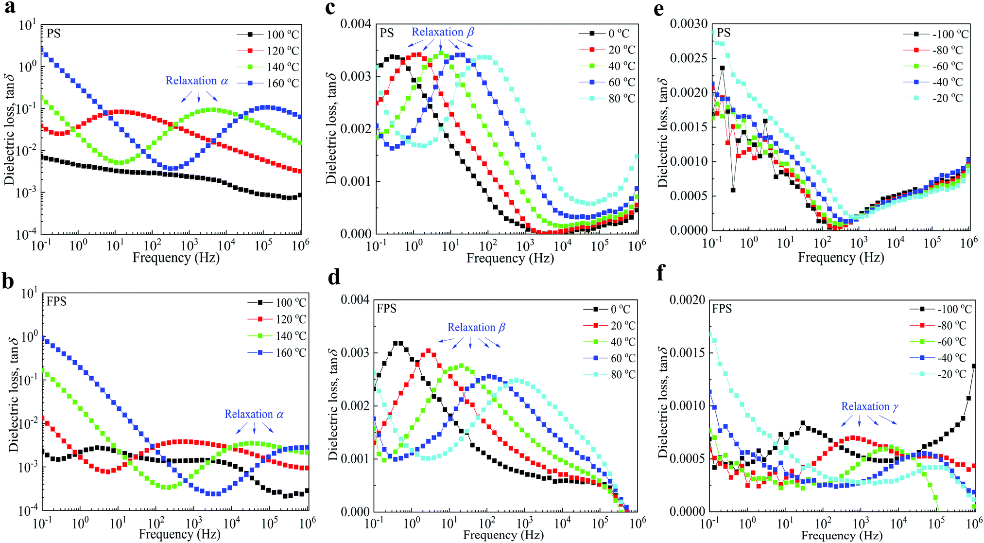 | ||
| Fig. 3 Dependence of dielectric loss tangents of PS and FPS on frequency in a wide temperature range of −100 to 160 °C. (a and b) Dependence of dielectric loss and relaxations of PS (a) and FPS (b) at a high temperature range of 100–160 °C. (c and d) Dependence of dielectric loss and relaxations of PS (c) and FPS (d) at a mid-temperature range of 0–80 °C. (e and f) Dependence of dielectric loss and relaxations of PS (e) and FPS (f) at a low temperature range of −100 to −20 °C. | ||
Therefore, as compared with PS, FPS has a larger relative permittivity, higher breakdown strength, along with deeper traps with increased activation energy. These characteristics contribute to higher charge storage capability, which generates stronger electrets with long-term stability that is helpful in manipulating OFET performance.
In order to investigate the dielectric dominated electrical performance of OFETs and verify the application potential of FPS as a gate dielectric, C12-BTBT is applied as the p-channel organic semiconductor, with PS and FPS separately serving as the gate dielectrics to form a semiconductor/insulator vertical bi-layer structure. A top-contact/bottom-gate structure on a highly n-doped Si wafer (with 300 nm thermally grown SiO2) is utilized. The transfer and output performances of C12-BTBT/PS OFET are shown as Fig. 4a and b, respectively, in which the line with red-squares in Fig. 4a indicates the performance of as-prepared OFET without gate stress. The on-current of the C12-BTBT/PS transistor reaches 6.39 × 10⁻⁴ A in a saturation regime (Vd = −60 V), and the on/off ratio is 2 × 10⁶, with a threshold voltage of −26 V. By applying the equation,
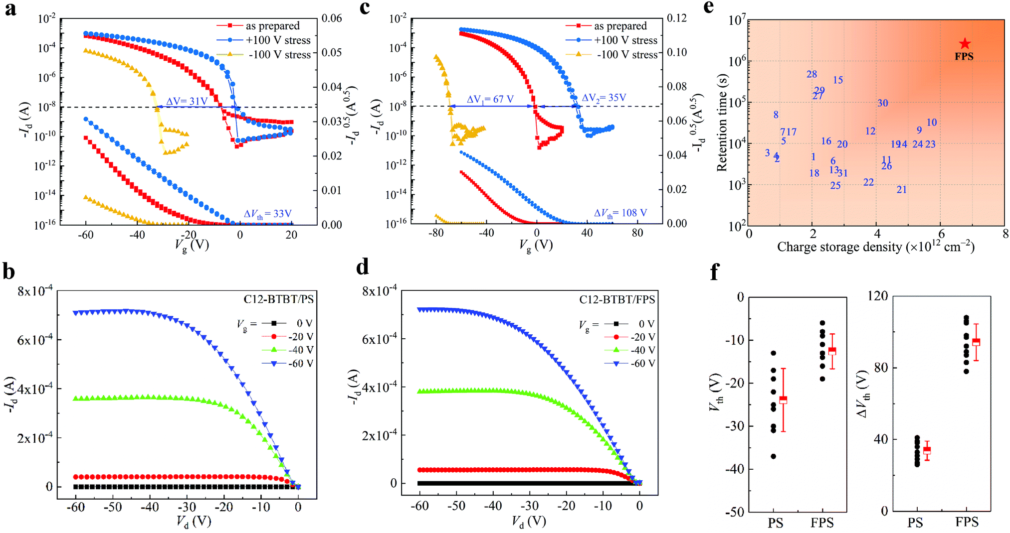 | ||
| Fig. 4 OFET performance of C12-BTBT/PS and C12-BTBT/FPS. (a) Transfer characteristics of C12-BTBT/PS OFET with ±100 V and without pretreatment by gate stress. (b) Output characteristics of the as-prepared C12-BTBT/PS OFET. (c) Transfer characteristics of C12-BTBT/FPS OFET with ±100 V and without pre-treatment by ±100 V gate stresses. (d) Output characteristics of the as-prepared C12-BTBT/FPS OFET. (e) Charge storage density and retention time of polymeric gate dielectrics applied in OFETs. The reference numbers are provided in Table S2 (ESI†). (f) Statistics of the threshold voltage Vth, and shift of the threshold voltage ΔVth for C12-BTBT/PS, and C12-BTBT/FPS transistors. The data are obtained from 10 devices, and presented with mean values and standard deviation. | ||
For OFET with an FPS gate dielectric, the transfer and output characteristics are shown in Fig. 4c and d, respectively. The on-current reaches 9.13 × 10⁻⁴ A, which shows a slight increase compared to the C12-BTBT/PS device. The on/off ratio is 9 × 10⁶, and the threshold voltage is −14 V. The maximum field-effect mobility reaches 11.2 cm2 s−1 V−1, while the average mobility is 10.3 cm2 s−1 V−1. A comparison of the device performance between FPS and PS based OFETs is shown in Table S3 (ESI†). From the statistical data, we conclude that the as prepared C12-BTBT/FPS OFET shows better device performance compared to the C12-BTBT/PS device, as a larger on current is achieved towards 10−3 A, and the threshold voltage is decreased by nearly 50% with a 3.5 times increased on/off ratio.
These results are contributed to by the modification of the semiconductor/insulator interface by the introduction of the fluorine atoms in dielectrics, as a gate dielectric with strong polarity leads to decreased threshold voltage and operation voltage. However, dielectrics with high permittivity could induce broadened energetic disorder of localized states in semiconductors near the interface, leading to decreased field effect mobility of the transistor.68 As a result, average mobility of FPS based OFET is 10.3 cm2 s−1 V−1, which is slightly smaller than that of the PS based OFET (11.9 cm2 s−1 V−1).
The OFET performance can be manipulated by gate bias-stress, and this method is widely applied in non-volatile memories as the programming and erasing processes.42,69 In order to analyze the charge storage capability dominated memory characteristics of OFET devices and reveal the related mechanism, in this work, ±100 V gate stresses are applied to both C12-BTBT/PS and C12-BTBT/FPS OFETs, and the results are shown in Fig. 4a and c, respectively.
In Fig. 4a, the transfer curve shifts towards the direction of positive Vg when stressed at +100 V gate bias, and the sub-threshold swing is improved with an increased on-current of 9.44 × 10⁻⁴ A, while the threshold voltage is shifted to −3 V. When a −100 V gate bias is stressed, the transfer curve shifts towards negative Vg, and the threshold voltage is −36 V. Consequently, the memory window referring to the ΔVth of the C12-BTBT/PS device is 33 V. For the C12-BTBT/FPS OFET in Fig. 4c, the threshold voltage can shift across Vg = 0 V to realize a positive value, as a result of the strong electronegativity generated by the introduced F atom, which leads to the accumulation of more electrons in the dielectric. These results are in accordance with the reported results of fluorinated polymers such as P3TFMS,40 and P4VP(2-hydroxyanthracene),22 as positive threshold voltage of ∼15 V and ∼75 V are realized correspondingly after positive gate stresses. Interestingly, for C12-BTBT/PS, the shift of transfer curve towards negative Vg also becomes more dramatic when a −100 V gate bias is stressed as compared with C12-BTBT/PS, and the threshold voltage reaches −69 V, forming ΔVth = 108 V. It should be noted that the negative shift (67 V) is comparatively larger than the positive shift (35 V). However, this phenomenon does not violate the conclusion that FPS introduces more electron traps obtained in Fig. 2c, as the p-channel C12-BTBT suppresses electron migration and injection into the polymeric gate dielectric. Compared to ΔVth = 33 V of the C12-BTBT/PS device, this data shows a 2.27 times increase, and is larger than those reported in recent work (Fig. S3 and Table S2, ESI†). The statistical results in Fig. 4f show that the average ΔVth of the FPS based OFET is 94.3 V, while that of PS is 33.8 V. Thus, the memory window of OFET is greatly optimized by the FPS dielectric polymer.
In fact, the shifting range of threshold voltage depends on the intensity of the dielectric electret, thus the memory window is dominated by trap density of the dielectric. Moreover, considering that the memory window depends on the thickness of SiO2 which may vary between investigations, charge storage density (Δn) of the polymeric dielectric is compared, as shown in Fig. 4e. Δn of FPS reaches 6.8 × 1012 cm−2, showing obvious improvement against other polymers. Compared to OFETs with a PS gate dielectric, the enlarged trap density in FPS (as demonstrated in Fig. 2c) generates a stronger electric field in the vicinity of the semiconductor layer, which triggers a tremendous shift of the transfer curve under gate biases, resulting in ΔVth = 108 V for the C12-BTBT/FPS device. In addition, we have investigated FPS with two molecular weights, Mw = 1300 kDa (PDI = 1.3) and Mw = 1600 kDa (PDI = 1.25), and no apparent difference is found between them in terms of electret performance. Upon comparing FPS of different molecular weights with PS, all of which have high molecular weights over 1000 K, we could carefully conclude that the charge trapping is not due to end chain groups. Rather, the charge trapping is mainly contributed to by the F substituted benzene ring.
Long-term memory stability is another key factor that defines whether an OFET realizes application potential, as volatile characteristics lead to data loss. Advances in the operational stability of OFETs against gate stresses are commonly reported by applying fluorinated polymers.30,31,33,70 However, excellent gate electret stability for long-term operation is difficult to realize.24 In this work, memory stability is investigated with gate stresses of Vg = ±100 V on both C12-BTBT/PS and C12-BTBT/FPS OFETs. The devices were kept in ambient conditions with relative humidity of 45%. The retention characteristics of C12-BTBT/PS and C12-BTBT/FPS OFETs are investigated with a time interval of up to 104 s for testing Id after programming and erasing, the results are demonstrated in Fig. 5a. For the C12-BTBT/PS device, both the programmed and erased states experience half an order decrease at the end of 104 s. Comparatively for C12-BTBT/FPS devices, both the programmed and erased states are stable during the 104 s duration with an on/off ratio ∼107. Id of both programmed and erased states becomes even more stable at the end of 104 s, indicating balanced electret charges after unstable charges are depleted. Thus, we could expect a longer retention time for C12-BTBT/FPS OFETs. Considering the limited access of the testing equipment, further long-term memory stability of up to one month is characterized in Fig. 5b and c. Fig. 5b shows the memory stability of C12-BTBT/PS devices. It is noticed that the transfer curve is shifted towards positive Vg, and the threshold voltage reaches −2 V. For as long as one month, the shifted Vg is retained and demonstrates a well-defined overlap of transfer curves at each testing duration, which indicates excellent memory stability under positive bias stresses. However, the differences in transfer characteristics between the as-prepared and positive stressed OFETs are quite small, and no obvious discrimination can be drawn in terms of threshold voltage. Besides, further investigation indicates that this positive memory stability might not be contributed by the gate dielectric PS, as the oxidation of semiconducting C12-BTBT also shifts the transfer curve towards Vg = 0 V.71
 | ||
| Fig. 5 Memory stability of C12-BTBT/PS and C12-BTBT/FPS OFET devices. (a) Retention characteristics of C12-BTBT/PS and C12-BTBT/FPS OFETs after programming and erasing. Ambient stabilities of C12-BTBT/PS (b) and C12-BTBT/FPS (c) OFETs with positive and negative electrets, D represents day. Repeatability over 100 cycles of C12-BTBT/PS (d) and C12-BTBT/FPS (e) OFETs with positive and negative electrets, C represents cycle. | ||
For situations of negative gate stresses, the results become non ideal as an obvious retreat towards the as-prepared characteristics is observed continuously over one month. Even though the shift of threshold voltage is sufficiently large after −100 V stress, the unstable long-term response would greatly restrict its application potential for OFET memories.
In Fig. 5c, a much more stable response to both positive and negative gate stresses is realized by replacing PS with FPS as the gate dielectric. It is noticed that the transfer curve shifts to positive Vg with a threshold voltage of ∼40 V. This shift becomes solid over one month, which shows only slight recovery within 7 V. Thus, the programming characteristic of a memory device is enhanced compared to the C12-BTBT/PS device, as a larger discrimination against the origin state along with higher stability is achieved. When −100 V is stressed on the C12-BTBT/FPS transistor, its transfer curve shifts towards negative Vg, forming a memory window larger than 100 V. The memory stability under −100 V is greatly enhanced compared to C12-BTBT/PS devices, and no obvious recovery is observed during one month in ambient conditions.
The memory stability of OFETs is dominated by the lasting duration of the electret, which is controlled by the trap energy of a dielectric film.46,72–74 The newly generated deeper traps in FPS increase the average trap energies of both electrons and holes (Fig. 2c), leading to an enlarged activation energy to avoid charge detrapping. As a result, the retention time of the trapped charges is greatly increased, which finally leads to the enhanced bias-stress stability of FPS transistors (Fig. 5c).
It must be noted that the memory stability is synergistically influenced by many factors. Hydrophobicity is another important factor, and is increasingly important for OFETs in ambient conditions.14,26 The water contact angle results in Fig. 1b demonstrate that the hydrophobic surface of FPS can prevent water from invading, leading to decreased leakage current, which consequently increases the OFET memory stability against moisture in ambient conditions.
Repeat stability is another important parameter that defines whether a memory device maintains its initial programming signal. In this work, the repeat stability of C12-BTBT/PS and C12-BTBT/FPS transistors is compared over 100 cycles of gate voltage scanning, as shown in Fig. 5d and e. It is noticed that both of the devices retain good stability. The C12-BTBT/FPS device shows minor degradation, indicating both the “programming” and “erasing” processes are maintained against operational gate voltage.
However, the semiconductors C12-BTBT and PCDTPT investigated in this work are p-channel semiconductors, and electron migration is significantly suppressed. We found that the electron current is orders of magnitude smaller than the hole current, which results in smaller electron charge injection and trapping. After repeated charge injection and depletion, the bias stress leads to poorer electron injection. This scenario leads to poor cyclic repeatability.
In order to verify the universality of FPS for high performance transistors and memories, the conjugated polymer PCDTPT is selected as the semiconductor to form solution blends with PS and FPS separately. The OFETs of PCDTPT/PS (PS 95 wt%) and PCDTPT/FPS (FPS 95 wt%) are fabricated by one-step spin coating. It should be noted that 5:95 is the optimized blending ratio after investigating four ratios: pure PCDTPT, 50:50, 20:80 and 5:95. The OFET performance is demonstrated in Fig. S4 in the ESI,† showing the largest field-effect mobility and on/off ratio of 5:95. During device fabrication, vertical phase separation between PCDTPT and PS (or FPS) occurred and PCDTPT is partly enriched at the top part of the blend, while in another part of the film the trace PCDTPT molecules within the insulator matrix could facilitate the charge trapping (Fig. S5, S6, and Table S4, ESI†). It is noticed that the field effect mobility, on/off ratio and threshold voltage of the two devices (PCDTPT/PS and PCDTPT/FPS) are nearly the same. However, the memory window of PCDTPT/FPS device is 82 V, much larger than 35 V of the PCDTPT/PS device. These results are in accordance with the devices of C12-BTBT/PS and C12-BTBT/FPS in Fig. 4, as the FPS gate dielectric leads to an enlarged memory window.
The memory stabilities of PCDTPT/PS and PCDTPT/FPS devices in ambient conditions are shown in Fig. S7 (ESI†). After treatment with positive and negative bias stresses, PCDTPT/PS OFETs experience an obvious shift towards positive Vth over one month. In accordance with C12-BTBT/FPS devices, the transfer characteristics of PCDTPT/FPS after stressing ±100 V gate biases are maintained within one month, forming a memory window of 76 V. Thus, the universality of FPS for high performance transistors and memories is verified with semiconducting systems of both small molecules and polymers.
Conclusions
In this work, a new polymeric dielectric atactic FPS is synthesized through radical polymerization, which is found to have high charge storage capability to achieve a highly stable electret. FPS is featured with a high density of deep bulk charge traps, high electrical breakdown strength, high thermal stability and hydrophobicity. Using FPS thin films deposited from solution as the gate dielectric and electret layer, OFETs with C12-BTBT as the semiconductor layer show high mobility up to 11.2 cm2 V−1 s−1, a large on/off ratio of 107, and a small threshold voltage. Compared with the model electret PS, increased trap density and trap energy for both the electrons and holes in FPS contribute to a high sheet charge density of 6.8 × 1012 cm−2, a new record for an electret layer for OFET applications. OFETs with FPS can work with a wide memory window >100 V with tremendously improved electret stability over one month in ambient conditions. Due to the deep bulk traps and hydrophobic surface preventing moisture from invading, this air-stable electret shows a bright future for electronic applications.Experimental section
Dielectric and thermal characterization
The water contact angle of the PS and FPS films (coated on n-doped Si wafer with 300 nm thermally grown SiO2) were measured using a DSA-X tester (Betop Scientific, China). The DSC tests were performed with a DSC 822e-700 (Mettler Toledo, Switzerland) at temperatures ranging from 50 to 350 °C with a ramping rate of 10 °C min−1. The TGA tests were performed with a TGA/SDTA 851 (Mettler Toledo, Switzerland) at a temperature ramping rate of 10 °C min−1. The UV-visible absorption spectra were obtained by a PE Lambda 35 UV/Vis/NIR spectrophotometer and the films were fabricated on fused glass substrates. Electrical breakdown characteristics of PS and FPS were performed with a ϕ = 25 mm sphere-plate electrode clamped to a thickness of 150 μm sample, and the sphere electrode is connected to a high voltage source for up to 100 kV DC voltage, with the plate electrode grounded. During the test, the sample with electrode was immersed into insulating oil to avoid surface discharging. The relative permittivity and dielectric loss tanδ of PS and FPS were obtained by applying 1 V AC small signal onto the sample with the test system of broadband dielectric spectroscopy (Novo control concept 80, Germany) in nitrogen (with Alpha – A sample cell) in the frequency range from 10−1 to 106 Hz, and temperature range from −100 to 160 °C, the details of the test system and sample cell can be found in the ESI†, Fig. S8. In the ISPD test, the needle charging voltage was 10 kV, the grid bias voltage was 5 kV, the charging duration was 300 s and the discharging duration was 28800 s (8 h). The thickness of 150 μm sample was used in tests of ISPD, breakdown, relative permittivity and dielectric loss, which was prepared by melt thermal pressing with a plate vulcanizing machine. The powder sample was preheated above 270 °C for 10 min. Afterwards, gradient pressures were stressed on to the sample with the procedure of 10 MPa for 5 min, 15 MPa for 5 min, and 20 MPa for 5 min, then the film was cooled down to room temperature for further experiments.
Synthesis and device fabrication
For the synthesis of FPS, 4-fluorostyrene (24.40 g, 0.2 mol) and azoisobutyronitrile (AIBN) (3.28 mg, 20 μmol) were sealed in an ampoule with a magnetic stirrer in a glove box. The mixture was heated to 95 °C for 10 min to initiate the polymerization. Then the polymerization was carried out at 65 °C. After 24 h, the afforded mixture was dissolved in chloroform and poured into a large amount of ethanol to obtain the polymer as a white precipitate. The afforded polymer was purified through being dissolved in chloroform and precipitated in ethanol three times. Finally, the polymer was dried under vacuum at 40 °C to a constant weight. The molecular weight and the molecular weight distribution of the polymers were measured in THF at 40 °C by a TOSOH HLC-8220 GPC instrument, the results are shown in Fig. S2 in the ESI,† indicating Mw = 1600 kDa, PDI = 1.25.PS (Mw = 2000 kDa, PDI = 1.3) was purchased from Sigma-Aldrich; PCDTPT was purchased from 1-Material; both PS and PCDTPT were applied without further treatment. C12-BTBT was laboratory synthesized, and the 1H spectrum of C12-BTBT is shown in Fig. S9 (ESI†).
The solubility of FPS is similar to that of polystyrene, which can be dissolved in o-dichlorobenzene, THF, chloroform, dichloromethane etc. In this work, o-dichlorobenzene is selected as the solvent to ensure good solubility, crystallization, and vertical phase separation of semi-crystalline PCDTPT.
Bottom-gate/top-contact OFETs were fabricated on n-type-doped Si/SiO2 (300 nm) substrates. The substrate was cleaned ultrasonically with distilled water, acetone, and isopropanol, respectively, and then dried with nitrogen before device fabrication. For OFETs with C12-BTBT as the charge transfer layer, PS or FPS were dissolved in o-dichlorobenzene to achieve a concentration of 5 mg mL−1, and then spin coated at 3000 rpm onto the Si/SiO2 substrate. The PS or FPS film was then annealed at 130 °C for 30 min, and cooled down to room temperature.21,75 A 50 nm C12-BTBT film was deposited onto PS or FPS via thermal evaporation under a vacuum atmosphere (<10−4 Pa) at 0.1 Å s−1, measured by a quartz crystal microbalance. For OFETs with PCDTPT serving as the channel layer, blends of PCDTPT/PS and PCDTPT/FPS at a weight ratio of 5:95 were dissolved into o-dichlorobenzene at 5 mg mL−1. The blended solution was spin-coated onto the Si/SiO2 substrate at 3000 rpm, and then annealed at an optimized temperature of 180 °C for 30 min (experimental results shown in Fig. S10 in the ESI†) to reach a stable morphology and dissipate the residual solvent and other volatile species. All the spin-coating and annealing processes were conducted in a nitrogen glove box. After forming the dielectric and semiconductor layers, gold source and grain electrodes with a thickness of 50 nm were thermally evaporated through shadow masks at 0.5 Å s−1. The identical channel length is 300 μm and the channel width is 3 mm.
Device characterization
The electrical characteristics of the OFETs were measured by an Agilent Keysight B2900A Quick IV system in ambient conditions at room temperature. The field-effect mobility and threshold voltage were extracted from the tested transfer characteristics in a saturation regime. The total capacity of FPS coated SiO2 is 10.5 nF cm−2, calculated by 1/Ctotal = (1/CFPS + 1/CSiO2), CFPS = ε0·εFPS/d, and εFPS = 2.85 which is obtained from Fig. 2f. The total capacity of PS coated SiO2 is 10.4 nF cm−2. To generate the gate electret, constant ±100 V gate stresses are applied separately with Vd = 0 V for 60 s onto the OFET devices. To be noted is that in OFETs with a p-channel semiconductor, a negative shift of Vth is finished within 1 s while a positive shift can take seconds, thus 60 s is applied to ensure complete charge trapping.Conflicts of interest
There are no conflicts to declare.Acknowledgements
This work was financially supported by the National Natural Science Foundation of China (51907148, 51873172, 21574103, 51673184), the China Postdoctoral Science Foundation (2018M643648), the Youth Fund of State Key Laboratory of Electrical Insulation and Power Equipment (EIPE19308), the Fundamental Research Funds for the Central Universities (xjh012019023), and the Natural Science Basic Research Plan in Shaanxi Province of China (2019JQ-070).References
- L. Bu, M. Hu, W. Lu, Z. Wang and G. Lu, Adv. Mater., 2017, 30, 1704695 CrossRef PubMed.
- J. C. Scott and L. D. Bozano, Adv. Mater., 2010, 19, 1452 CrossRef.
- K. J. Baeg, Y. Y. Noh, J. Ghim, S. J. Kang and D. Y. Kim, Adv. Mater., 2010, 18, 3179 CrossRef.
- Y. Iwasaki, A. Yamasaki and K. Ishihara, Biomaterials, 2003, 24, 3599 CrossRef CAS.
- M. K. Smith and K. A. Mirica, J. Am. Chem. Soc., 2017, 139, 16759 CrossRef CAS PubMed.
- D. Zhao, L. Duan, M. Xue, W. Ni and T. Cao, Angew. Chem., Int. Ed., 2009, 48, 6699 CrossRef CAS PubMed.
- M. Z. Elsabee, E. S. Abdou, K. S. A. Nagy and M. Eweis, Carbohydr. Polym., 2008, 71, 187 CrossRef CAS.
- L. L. Cui, M. H. Song, Y. X. Kong, L. Cheng, D. Wang, Y. H. Xiao and J. Jiang, J. Electrost., 2009, 67, 412 CrossRef CAS.
- Y. Chou, H. Chang, C. Liu and W. Chen, Polym. Chem., 2015, 6, 341–352 RSC.
- C. C. Shih, W. Y. Lee and W. C. Chen, Mater. Horiz., 2016, 3, 294 RSC.
- S. Wang, X. Jie, W. Wang, G. J. N. Wang and Z. Bao, Nature, 2018, 555, 83–88 CrossRef CAS PubMed.
- K. Yu, B. Park, G. Kim, C. Kim, S. Park, J. Kim, S. Jung, S. Jeong, S. Kwon and H. Kang, Proc. Natl. Acad. Sci. U. S. A., 2016, 113, 14261 CrossRef CAS PubMed.
- H. Dong, X. Fu, J. Liu, Z. Wang and W. Hu, Adv. Mater., 2005, 25, 6158 CrossRef PubMed.
- D. Natali and M. Caironi, Adv. Mater., 2012, 24, 1357 CrossRef CAS PubMed.
- S. Goffri, C. Müller, N. Stingelin-Stutzmann, D. W. Breiby, C. P. Radano, J. W. Andreasen, R. Thompson, R. A. J. Janssen, M. M. Nielsen and P. Smith, Nat. Mater., 2006, 5, 950 CrossRef CAS PubMed.
- P. Wei, S. Li, D. Li, Y. Han, X. Wang, C. Xu, Y. Yang, L. Bu and G. Lu, Nano Res., 2018, 11, 5835 CrossRef CAS.
- H. H. Choi, W. H. Lee and K. Cho, Adv. Funct. Mater., 2012, 22, 4833 CrossRef CAS.
- H. Shen, Y. Zou, Y. Zang, D. Huang, W. Jin, C. Di and D. Zhu, Mater. Horiz., 2018, 5, 240–247 RSC.
- J. Zaumseil and H. Sirringhaus, Chem. Rev., 2007, 107, 1296 CrossRef CAS PubMed.
- Z. Song, Y. Tong, X. Zhao, H. Ren, Q. Tang and Y. Liu, Mater. Horiz., 2019, 6, 717–726 RSC.
- Y. Ren, Y. Zhu, D. Li, P. Wei, W. Lu, L. Bu and G. Lu, J. Mater. Chem. C, 2019, 7, 12862 RSC.
- Y. Chou, Y. Chiu, W. Lee and W. Chen, Chem. Commun., 2015, 51, 2562 RSC.
- Y. H. Chou, N. H. You, T. Kurosawa, W. Y. Lee and W. C. Chen, Macromolecules, 2012, 45, 6946 CrossRef CAS.
- L. Junghwi, M. Honggi, P. Namwoo, J. Heejeong, H. Singu, K. Se Hyun and L. Hwa Sung, ACS Appl. Mater. Interfaces, 2015, 7, 25045 CrossRef PubMed.
- S. Park, S. H. Kim, H. H. Choi, B. Kang and K. Cho, Adv. Funct. Mater., 2019, 1904590 CrossRef.
- B. J. Jung, K. Lee, J. Sun, A. G. Andreou and H. E. Katz, Adv. Funct. Mater., 2010, 20, 2930 CrossRef CAS.
- Y. Yu, Q. Ma, H. Ling, W. Li, R. Ju, L. Bian, N. Shi, Y. Qian, M. Yi, L. Xie and W. Huang, Adv. Funct. Mater., 2019, 1904602 CrossRef CAS.
- C. Ying-Hsuan, C. Yu-Cheng and C. Wen-Chang, Chem. Commun., 2014, 50, 3217 RSC.
- K. J. Baeg, Y. Y. Noh, J. Ghim, B. Lim and D. Y. Kim, Adv. Funct. Mater., 2008, 18, 3678 CrossRef CAS.
- Y. Baek, S. Lim, E. J. Yoo, L. H. Kim, H. Kim, S. W. Lee, S. H. Kim and C. E. Park, ACS Appl. Mater. Interfaces, 2014, 6, 15209 CrossRef CAS PubMed.
- S. H. Kim, J. Kim, S. Nam, H. S. Lee, S. W. Lee and J. Jang, ACS Appl. Mater. Interfaces, 2017, 9, 12637 CrossRef CAS PubMed.
- C. C. Shih, Y. C. Chiu, W. Y. Lee, J. Y. Chen and W. C. Chen, Adv. Funct. Mater., 2015, 25, 1511 CrossRef CAS.
- K. Jiye, J. Jaeyoung, K. Kyunghun, K. Haekyoung, K. Se Hyun and P. C. Eon, Adv. Mater., 2014, 26, 7241 CrossRef PubMed.
- K. N. N. Unni, R. D. Bettignies, S. Dabos-Seignon and J. M. Nunzi, Appl. Phys. Lett., 2004, 85, 1823 CrossRef CAS.
- B. Stadlober, M. Zirkl, M. Beutl, G. Leising, S. Bauer-Gogonea and S. Bauer, Appl. Phys. Lett., 2005, 86, 169 CrossRef.
- W. Xu, G. Yang, L. Jin, J. Liu, Y. Zhang, Z. Zhang and Z. Jiang, ACS Appl. Mater. Interfaces, 2018, 10, 11233 CrossRef CAS PubMed.
- B. Qiao, X. Wang, S. Tan, W. Zhu and Z. Zhang, Macromolecules, 2019, 52, 9000 CrossRef CAS.
- Y. J. Jeong, D. Yun, S. Nam and J. Jang, Appl. Surf. Sci., 2019, 481, 642 CrossRef CAS.
- D. Lei, H. S. Sun, J. T. Wang, W. Y. Lee and W. C. Chen, J. Polym. Sci., Part A: Polym. Chem., 2015, 53, 602 CrossRef.
- P. Evan, K. Tejaswini, S. Q. Zhang, H. E. Katz and D. H. Reich, Appl. Phys. Lett., 2019, 114, 23301 CrossRef.
- W. Li, F. Guo, H. Ling, H. Liu, M. Yi, P. Zhang, W. Wang, L. Xie and W. Huang, Small, 2018, 14, 1701437 CrossRef PubMed.
- Y. H. Chou, S. Takasugi, R. Goseki, T. Ishizone and W. C. Chen, Polym. Chem., 2013, 5, 1063 RSC.
- S. H. Kim, K. Kim, H. Kim and E. P. Chan, Phys. Chem. Chem. Phys., 2015, 17, 16791 RSC.
- N. Shi, L. Dong, X. Jin, W. Wu, J. Zhang, M. Yi, L. Xie, F. Guo, Y. Lei and C. Ou, Org. Electron., 2017, 49, 218 CrossRef CAS.
- J. Lin, W. Li, Z. Yu, M. Yi, H. Ling, L. Xie, S. Li and W. Huang, J. Mater. Chem. C, 2014, 2, 3738 RSC.
- J. C. Hsu, W. Y. Lee, H. C. Wu, K. Sugiyama, A. Hirao and W. C. Chen, J. Mater. Chem., 2012, 22, 5820 RSC.
- P. Graham, M. Stone, A. Thorpe, T. G. Nevell and J. Tsibouklis, J. Fluorine Chem., 2000, 104, 29–36 CrossRef CAS.
- H. Ling, L. Wen, H. Li, M. Yi, L. Xie, L. Wang, Y. Ma, B. Yan, F. Guo and H. Wei, Org. Electron., 2017, 43, 222–228 CrossRef CAS.
- S. Li, Y. Zhu, D. Min and G. Chen, Sci. Rep., 2016, 6, 32588 CrossRef CAS PubMed.
- F. Zhou, J. Li, M. Liu, D. Min, S. Li and R. Xia, IEEE Trans. Dielectr. Electr. Insul., 2016, 23, 1174 CAS.
- Y. Zhu, S. Li and D. Min, IEEE Trans. Dielectr. Electr. Insul., 2017, 24, 1625 CAS.
- J. G. Simmons and M. C. Tam, Phys. Rev. B: Solid State, 1973, 8, 3706–3713 CrossRef.
- J. Li, F. Zhou, D. Min, S. Li and R. Xia, IEEE Trans. Dielectr. Electr. Insul., 2015, 22, 1723 CAS.
- G. Chen, J. Zhao, S. Li and L. Zhong, Appl. Phys. Lett., 2012, 100, 222904 CrossRef.
- F. Zheng, J. Dong, Y. Zhang, Z. An and Q. Lei, Appl. Phys. Lett., 2013, 102, 12901 CrossRef.
- Y. Du, Y. Lv, C. Li, M. Chen, Y. Zhong, S. Zhang and Z. You, J. Appl. Phys., 2012, 111, 222 Search PubMed.
- S. Li, D. Min, W. Wang and G. Chen, IEEE Trans. Dielectr. Electr. Insul., 2016, 23, 2777 CAS.
- G. C. Montanari, G. Mazzanti, F. Palmieri, A. Motori, G. Perego and S. Serra, J. Phys. D: Appl. Phys., 2001, 34, 2902 CrossRef CAS.
- N. Zhao, Y. Nie and S. Li, AIP Adv., 2018, 8, 45103 CrossRef.
- N. Zhao, N. Yongjie and L. Shengtao, J. Mater. Sci.: Mater. Electron., 2018, 29, 12850 CrossRef CAS.
- D. Min, Y. Li, C. Yan, D. Xie, S. Li, Q. Wu and Z. Xing, Polymers, 2018, 10, 1012 CrossRef PubMed.
- D. Fabiani and L. Simoni, IEEE Trans. Dielectr. Electr. Insul., 2005, 12, 11 CrossRef.
- L. Bo, P. Xidas and E. Manias, ACS Appl. Nano Mater., 2018, 1, 3520 CrossRef.
- G. D. Peppas, A. Bakandritsos, V. P. Charalampakos, E. C. Pyrgioti, J. Tucek, R. Zboril and I. F. Gonos, ACS Appl. Mater. Interfaces, 2016, 8, 25202 CrossRef CAS PubMed.
- Z. Lv, X. Wang, K. Wu, X. Chen, Y. Cheng and L. A. Dissado, IEEE Trans. Dielectr. Electr. Insul., 2013, 20, 337 CAS.
- B. X. Du, J. W. Zhang, Y. Gao, B. X. Du, J. W. Zhang and Y. Gao, IEEE Trans. Dielectr. Electr. Insul., 2012, 19, 755 CAS.
- K. L. Ngai, A. K. Jonscher and C. T. White, Nature, 1979, 277, 185 CrossRef CAS.
- J. Veres, S. D. Ogier, S. W. Leeming, D. C. Cupertino and S. M. Khaffaf, Adv. Funct. Mater., 2010, 13, 199 CrossRef.
- M. Melissa, F. Antonio, L. Michael, H. E. Katz and T. J. Marks, J. Am. Chem. Soc., 2003, 125, 9414 CrossRef PubMed.
- W. L. Kalb, T. Mathis, S. Haas, A. F. Stassen and B. Batlogg, Appl. Phys. Lett., 2007, 90, 606 CrossRef.
- Y. Qiu, P. Wei, Z. Wang, W. Lu, Y. Jiang, C. Zhang, Y. Qu and G. Lu, Phys. Status Solidi RRL, 2018, 12, 1800297 CrossRef.
- R. Naber, B. de Boer, P. Blom and D. de Leeuw, Appl. Phys. Lett., 2005, 87, 166 CrossRef.
- T. T. Dao, T. Matsushima and H. Murata, Org. Electron., 2012, 13, 2709 CrossRef CAS.
- S. Tsuyoshi, Y. Tomoyuki, Z. Ute, K. Hagen, B. Siegfried, T. Ken, T. Makoto, S. Takayasu and S. Takao, Science, 2009, 326, 1516 CrossRef PubMed.
- P. Wei, Y. Hu, Y. Zhu, Y. Jiang, X. Feng, S. Li, L. Bu, X. Yang and G. Lu, Adv. Electron. Mater., 2018, 4, 1800339 CrossRef.
Footnote |
| † Electronic supplementary information (ESI) available. See DOI: 10.1039/d0mh00203h |
| This journal is © The Royal Society of Chemistry 2020 |