
 Open Access Article
 This Open Access Article is licensed under a Creative Commons Attribution-Non Commercial 3.0 Unported Licence
Delineating the enhanced efficiency of carbon nanomaterials including the hierarchical architecture of the photoanode of dye-sensitized solar cells†
Venkatesan
Srinivasan‡
a,
Jagadeeswari
Sivanadanam‡
*b,
Kothandaraman
Ramanujam‡
 b and
Mariadoss
Asha Jhonsi‡
*a
b and
Mariadoss
Asha Jhonsi‡
*a
aDepartment of Chemistry, B. S. Abdur Rahman Crescent Institute of Science and Technology, Vandalur, Chennai – 600 048, Tamil Nadu, India. E-mail: jhonsiasha@gmail.com
bDepartment of Chemistry, Indian Institute of Technology Madras, Chennai –600 036, Tamil Nadu, India. E-mail: Jagadhi333@gmail.com
First published on 15th October 2020
Abstract
Dye-sensitized solar cells are economical and easy to fabricate in comparison to silicon-based solar cells. The visible light sensitizer dye is the main component of DSSCs, the performance of which can be enhanced if the TiO2 semiconductor is engineered to maximize the utilization of the dye together with its easy regeneration from its oxidized form. In this study, a hierarchical porous architecture was imparted to the TiO2 photoanode using size-selected (1.5 to 3 nm) carbon nanomaterials (CNMs). This porous structure enhanced the accessibility of the dye to the electrolyte. Using the N719 dye as a model system, the effect of the hierarchical porous structure was demonstrated. The inclusion of CNMs together with TiO2 enhanced the short circuit current density by 31% and power conversion efficiency (PCE) by 46% compared to the CNM-free DSSCs.
Introduction
There is a continuous surge in the demand for energy due to the energy-intensive activity of human beings. Consequently, the non-replenishable sources are insufficient for the future expansion of the energy economy, which has motivated researchers to explore environmentally benign renewable energy sources. Therefore, harnessing the inexhaustible and clean energy source, solar energy, via photovoltaics occupies the central stage of renewable energy research.1 In the past two decades, significant advancement in the field of photovoltaics and efficiencies as high as 40% have been achieved by multijunction solar cell technologies. Among the various photovoltaic options, dye-sensitized solar cells (DSSCs) are considered to be inexpensive due to their ease of fabrication and use of ubiquitously available materials in their fabrication.2In DSSCs, besides the dye, wide bandgap semiconductors such as TiO2 and ZnO play a pivotal role in light harvesting. TiO2 offers a conducting pathway for transporting electrons from the excited state (lowest unoccupied molecular orbital (LUMO)) of the dye to the conductive back contact via its conduction band (CB) and anchors sufficient dye/photosensitizers via its high surface area. Thus, energy level matching of the dye–semiconductor interface, and rationally designed semiconductor films (to reduce the loss of illuminated light and loss of injected electrons by recombination with holes, defects and crystal boundaries) are essential. A straightforward way to significantly enhance the performance of DSSCs is by manipulating the morphology and crystal phase of the semiconductor film. In the past, photoanodes were improvised using nano-architectures,3–5 light-scattering layers,6,7 compositing with another semiconductor8–10 or graphene,11,12 doping,13–15 interfacial engineering,16,17 and TiCl4 post-treatment methods.18,19 For instance, various nanoforms of ZnO were used as cascading co-sensitized nanomaterials, which enhanced the efficiency of dye-sensitized solar cells.20,21 Also, vanadium-doped TiO2 was used to fabricate the working electrode in a DSSC via the layer-by-layer method, which exhibited a remarkable performance compared to the bare TiO2 particles.22
Electron transfer within TiO2 particles occurs via two phenomena, i.e. percolation through the network of particles and thermal accessibility to high energy states. Thus, to improve the electron transport, TiO2 has been explored as various nanostructures such as nanotubes,23 nanowires,24 hierarchical structures,25 and specifically exposed facets.26 A film made of ∼20 nm-sized TiO2 nanoparticles generally allows the semiconductor layer to achieve energy level matching and host a sufficient amount of dye. In this architecture, the electron adopts a random walk process, encountering many grain boundaries, trap states, and defects, which results in significant electron recombination if the interface is not well engineered. One way to achieve improved PCE is to use hierarchical spheres of TiO2 to form a secondary structure, which is concentric spherical or three-dimensional in shape.27 These materials are known for their high light-harvesting and lower electron recombination28,29 since they promote light scattering and electron transport.
Novel materials such as plasmonic metal nanoparticles (gold and silver nanoparticles),30 photonic crystals,31 WO3-thiol-coated Au, and nanocarbon/carbon-based nanomaterials32 have been incorporated in the fabrication DSSCs. Among the various materials composited with TiO2 in DSSC devices, carbon-based nanomaterials33 are interesting owing to their synergistic and intrinsic properties. Carbon-based nanomaterials are generally manufactured via both top-down (electrodeposition, laser ablation, exfoliation of graphite, etc.) and bottom-up approaches (solvo/hydrothermal, microwave assisted, ultrasonic synthesis, etc.).34,35 It has been reported that the addition of a certain amount of nanocarbon to TiO2 can boost the efficiency of DSSC devices. For instance, Yu et al. achieved a PCE of up to 25% by incorporating 0.75 wt% of graphene with TiO2 nanosheets. Carbon nanotubes were also explored for their ability to reduce the charge recombination in DSSCs. Generally, graphene is preferable over 1D carbon nanotubes since the latter has fewer intermolecular forces and connections (point contact) with TiO2. Graphene exhibits an electron mobility of 15![[thin space (1/6-em)]](https://www.rsc.org/images/entities/char_2009.gif) 000 cm2 V−1 s−1, which exhibits a better performance compared to that of ZnO (200–1000 cm2 V−1 s−1) and TiO2 (0.1–4 cm2 V−1 s−1). According to the literature, the amount of carbon nanomaterials used is less than 1 wt% since loadings greater than this generally shield visible light from being harvested by the dyes, affecting the population of photogenerated electrons and PCE. Xiang et al. incorporated 0.2 wt% of nitrogen-reduced graphene oxide, which enhanced the PCE to 7.19% from 6.42% by circumventing electron recombination and the increasing the electron transfer efficiency.36 To alleviate the limitations associated with 1D nanomaterials, the 2D graphene (zero bandgap material) was explored as a bridge in a nanocrystalline semiconductor photoanode due to its lower transfer barrier, resulting in a lower recombination rate. Besides, the light-scattering effect of 2D graphene improved the short-circuit current density (Jsc) by 45% and PCE by 39% without sacrificing the open circuit voltage (Voc).37 A DSSC with the anatase TiO2@1.6 wt% reduced graphene oxide composite material prepared via a two-step hydrothermal method and stained by N719 dye showed a PCE of 7.68%, which was higher than that of the pristine anatase TiO2 (4.78%).38 Chen et al. demonstrated the effect of the graphene content on device performance, and they have attained an overall PCE of 7.1% at an optimum graphene content of 2 wt%, beyond which the light harvesting was affected negatively.39
000 cm2 V−1 s−1, which exhibits a better performance compared to that of ZnO (200–1000 cm2 V−1 s−1) and TiO2 (0.1–4 cm2 V−1 s−1). According to the literature, the amount of carbon nanomaterials used is less than 1 wt% since loadings greater than this generally shield visible light from being harvested by the dyes, affecting the population of photogenerated electrons and PCE. Xiang et al. incorporated 0.2 wt% of nitrogen-reduced graphene oxide, which enhanced the PCE to 7.19% from 6.42% by circumventing electron recombination and the increasing the electron transfer efficiency.36 To alleviate the limitations associated with 1D nanomaterials, the 2D graphene (zero bandgap material) was explored as a bridge in a nanocrystalline semiconductor photoanode due to its lower transfer barrier, resulting in a lower recombination rate. Besides, the light-scattering effect of 2D graphene improved the short-circuit current density (Jsc) by 45% and PCE by 39% without sacrificing the open circuit voltage (Voc).37 A DSSC with the anatase TiO2@1.6 wt% reduced graphene oxide composite material prepared via a two-step hydrothermal method and stained by N719 dye showed a PCE of 7.68%, which was higher than that of the pristine anatase TiO2 (4.78%).38 Chen et al. demonstrated the effect of the graphene content on device performance, and they have attained an overall PCE of 7.1% at an optimum graphene content of 2 wt%, beyond which the light harvesting was affected negatively.39
Based on the literature, it can be observed that the carbon nanomaterials (CNMs) used for the modification of the TiO2 photoanode are mostly prepared via tedious methods involving several steps and high energy consumption.40 Moreover, it is necessary to understand the structure and role of CNMs in the electron collection and transport at the interface of the photoanode of a DSSC device. The effects of size-selected CNMs have rarely been investigated. To the best of our knowledge, herein, the double dialysis method is employed for the first time for selecting size-controlled CNMs (∼2 nm-sized sheets) for application in DSSCs. In this study, different amounts of CNMs were incorporated in the photoanode to study the PCE of the resultant DSSCs. The loaded CNMs after heat treatment in air left a hierarchical pore structure, which enhanced the dye utilization and oxidized dye regeneration since the electrolyte access to the TiO2/dye interface was enhanced.
Experimental section
The details of the materials used are presented in the ESI.†Characterization techniques
1H NMR (500, 400 MHz) and 13C NMR (125, 100 MHz) spectra of the carbonaceous nanomaterials were recorded on a Bruker NMR spectrometer in D2O with tetramethylsilane as the internal standard. Fourier-transform infrared (FTIR) spectra were recorded on a JASCO FTIR-4100 spectrometer using a KBr cell and 1064 nm laser. Powder X-ray diffraction (PXRD) patterns were recorded using a Bruker D8 advance diffractometer equipped with a Cu Kα source (1.5406 Å). The solution-state absorption spectra were measured on a JASCO V-650 UV-visible spectrophotometer. Diffuse reflectance UV-Vis spectra were recorded employing a JASCO model V-570 solid-state UV-Vis spectrometer. Emission spectra were measured in CHCl3 solvent using a JASCO FP-6300 spectrofluorimeter. The photovoltaic performance (current density vs. voltage, J–V) was measured under one sun condition using a LOT Technologies solar simulator equipped with a 150 W xenon lamp and air mass (AM) 1.5 global filter, which provided a light power of 100 mW cm−2. The spectral intensity of the solar simulator was chosen considering the short-circuit current from the standard silicon solar cell (Type: RC2-1010, SN: 0520160006, SPD Laboratory, Inc.). A dark mask with a circle-shaped opening in the middle was placed on the DSSC to expose the active area of the DSSC to light. Electrochemical impedance spectroscopy (EIS) measurement was performed using a Metrohm Autolab 302N potentiostat/galvanostat (AUT86242) with the FRA32M module controlled by the NOVA 1.11 software. EIS fitting was performed using the ZSimWin 3.6 software.Synthesis of CNMs
Citric acid, sucrose and dithiobiurea in the weight ratio of 2:2:1 was initially dissolved in 50 mL of ultrapure water by sonication for 20 min. Then, the resulting colorless clear solution was transferred to a Teflon-lined stainless steel autoclave (100 mL capacity) and kept in a muffle furnace at 180 °C for 8 h.41 After the autoclave was cooled, the unreacted residues were removed by filtration, and the clear orange filtrate was centrifuged at 3000 rpm for 15 min to remove the minute suspended particles. Further, the clear supernatant solution was loaded in a separating funnel and washed with dichloromethane to remove the unreacted organic moieties. Finally, it was filtered using a 0.2 micron (pore size of 200 nm) cellulose syringe filter followed by volume reduction through distillation.
Size-selective separation of CNMs
The clear orange solution from the above step was dialyzed against ultrapure water using a dialysis membrane tube with a molecular weight cut off (MWCO) of 0.5–1 kDa (pore size, 1.5 nm) for 24 h. This process allowed small organic moieties with a size of less than 1.5 nm (maximum of 15 Å) to exit the dialysis tube. The dialysis bath water was changed every 6 h to avoid the accumulation/deposition of particles inside the dialysis tube wall. After 24 h of dialysis, particles with a size of >1.5 nm were left inside the tube. The product left inside the tube (>1.5–200 nm) was subjected to dialysis for a second time against ultrapure water in a dialysis membrane bag with an MWCO of 10–15 kDa (pore size, 3 nm) for another 24 h. The water outside turned pale yellow due to CNMs with a size ranging from 1.5 to 3 nm exiting the dialysis tube. This pale-yellow solution was collected and evaporated in a vacuum oven to obtain dark-brown colored shining particles called CNMs. The various stages of the synthesis of the size-selective CNMs are shown in the ESI† (Scheme S1).Preparation of CNM-loaded TiO2 film electrode
The photoanode was prepared following the reported method, and the typical preparation procedure is as follows. Fluorine-doped tin dioxide coated glass plates (FTO plates) were initially cut using a diamond cutter in the dimensions of 1.5 cm × 1.75 cm. The plates were immersed for 15 min in a soap solution, ultrapure water (two times), acetone, and isopropyl alcohol under sonication. The cleaned and dried plates were treated with 40 mM aqueous TiCl4 at 70 °C for 30 min. The TiCl4 treatment was repeated twice, and the plates were washed with double distilled water followed by ethanol. Further, the plates were heated in a muffle furnace at 500 °C for 30 min and allowed to cool to room temperature naturally. The TiCl4-treated conducting side of FTO was coated with transparent nano-titania paste loaded with various amounts of CNMs (5 mg of CNMs was dispersed in 5 mL of methanol and 0.1, 0.25, 0.5, 0.75, 1 and 1.5 mL of methanol dispersion was added to 100 mg titania paste and stirred for 12 h under ambient conditions) via the doctor blade technique using a mask with a circular hole. The thickness of the transparent layer was around 5–6 μm, and the coated area was 0.196 cm2. The TiO2-coated plates were heated at 500 °C for 30 min. Upon cooling the plate, a scattering layer of TiO2 was applied (Ti-nanoxide R/SP, Solaronix) via the doctor blade technique followed by heating at 400 °C for 20 min.Preparation of N719-dye/CNM-loaded TiO2 photoanode (FTO/TiO2-CNMs-N719)
FTO/TiO2 incorporated with different amounts of CNMs (0, 0.1, 0.25, 0.5, 0.75, 1 and 1.5 wt%) was immersed in N719 dye solution for 12 h (0.5 mM in 1:1 (v/v) ratio of acetonitrile and tertiary butanol solvent mixture) to ensure maximum uptake of dye by TiO2.
DSSC fabrication with FTO/TiO2-CNMs-N719 for J–V and EIS measurements
The FTO/TiO2-CNMs-N719 photoanode and Pt counter electrode were assembled into a sandwich-type cell with the help of a 60 μm hot-melt gasket frame (MS004610-10).42 Then the cell was filled with electrolyte through a hole left intentionally open at the back of the counter electrode. The liquid electrolyte consisted of LiI (0.1 M), I2 (0.05 M), t-butylpyridine (0.5 M) and 1-butyl-3-methyl imidazolium iodide (0.6 M) in a mixture of valeronitrile (15%) and acetonitrile (85%). A schematic representation of the fabricated device is shown in Scheme S2 (ESI†).Results and discussion
Citric acid was used as a carbon source for the graphene core, and the surrounding functional moieties of the CNMs were derived from sucrose and the presence of N and S heteroatoms from dithiobiurea, which increased the optical and electrochemical performances. Moreover, the precursor materials used for the synthesis of CNMs are easily accessible and inexpensive. The hydrothermal synthetic method employed yielded CNMs with a size of less than 3 nm with S and N functional groups tethered to them. The proposed mechanism for the formation of CNMs is shown in Scheme 1. Initially, dehydration occurs, followed by various processes, including hydrothermal degradation, polymerization and carbonization, leading to the nucleation and growth of CNMs. The structure of CNMs consists of two or three layers of nanometer-sized staked sheets of graphene covered with an amorphous shell bearing various functional moieties.35,43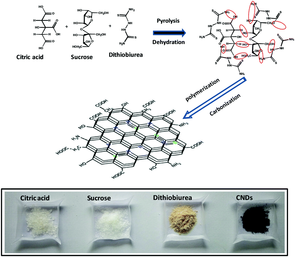 | ||
| Scheme 1 Proposed mechanism for the synthesis of CNMs. | ||
The SEM image (Fig. 1a) on a scale of 500 nm (60000× magnification) shows the transparent layered structure of CNMs. The energy dispersive X-ray spectrum (Fig. S1a, ESI†) confirms the presence of carbon, oxygen, nitrogen and sulphur. The elements originated from the precursors, and their atomic percentage is given in Fig. S1a (ESI†) (inset). HR-SEM was used to understand the surface morphology of the photoanode fabricated with and without CNMs, and the images are shown in Fig. 2. It can be observed that the surface of the film is smooth for TiO2, and for TiO2 with 0.5 wt% loading of CNMs, a few holes and surface cracks can be observed (Fig. 2a and b, respectively). This may due to the degassing of the surface functional groups of CNMs while heating the TiO2 films at 500 °C. EDAX did not detect any N and shows a trace of S (0.8%, Table S1, ESI†). Therefore, to understand the presence of carbon, CHNOS analysis was performed (Table S2, ESI†). The CHNOS analysis confirmed that only a trace amount of N and S was present. Therefore, most of the CNMs were incorporated into the photoanode, which were degassed during the annealing step, forming a porous TiO2 film. This probably enhanced the light scattering, similar to the hierarchical spheres of TiO2 forming a second structure that is concentric spherical or three-dimensional in shape.44
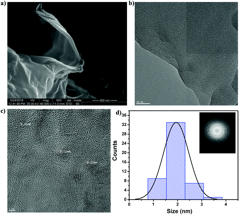 | ||
| Fig. 1 (a) HR-SEM image (at 60k magnification), (b) HR-TEM image (20 nm scale) of CNMs, (c) HR-TEM image (2 nm scale) of CNMs, and (d) particle size histogram (inset FFT image) derived from the image of (b). | ||
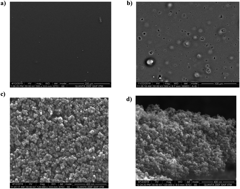 | ||
| Fig. 2 HR-SEM analysis of the bare transparent TiO2 film (a and c) and TiO2 with 0.5 wt% of CNMs (b and d). | ||
The three-dimensional shape and exact particle size details derived from the HR-TEM measurements are shown in Fig. 1b. The transparent layered structure of CNMs was confirmed through the HR-TEM micrographs, as shown in Fig. S1b (ESI†) (50 nm scale, 500000× magnification). The presence of particles with a size of 1.5 to 3 nm is discernible (Fig. 1b) from the particle size histogram (Fig. 1d). The presence of lattice fringes with spacings of 0.23 nm and 0.31 nm are possibly related to the (100) and (101) planes of CNMs, respectively (Fig. 1c). Further, the fast Fourier transform (inset of Fig. 1d) image shows the crystalline nature of the prepared CNMs. Atomic force microscopy (AFM) measurement gave the surface roughness with topographic details in non-contact mode (Fig. S1c, ESI†). It indicated the layered quasi-spherical sheet structure of CNMs. The root mean square roughness value obtained from the AFM measurement is 1.85 nm, indicating the smooth surface of the prepared CNMs.
AFM was also used to analyze the topographical details of the TiO2 photoanode prepared with and without CNMs (Fig. S2a and b (ESI†), respectively), and it was observed that the roughness for the bare TiO2 was around 8.3 nm, which increased to 14.60 nm upon loading with 0.5 wt% of CNMs. Profilometry is a useful tool to understand the surface roughness of a material and thickness of hierarchical porous architectures (thickness of the transparent TiO2 layer is around 5–6 μm, and the coated area is 0.196 cm2). Thus, profilometry was performed for the bare TiO2 photoanode and TiO2 loaded with 0.5 wt% CNMs. The thickness of the bare TiO2 and TiO2 loaded with 0.5 wt% CNMs is 9.6 μm and 8.5 μm, respectively. The average roughness of the TiO2 photoanode in the absence of CNMs is 234.36 nm, which increased in the presence of 0.5 wt% of CNMs to 462.14 nm. According to the profilometry images, it can be seen that the bare TiO2 film has a smooth surface (Fig. S3a, ESI†) compared to that of the film loaded with CNMs. Moreover, the film loaded with CNM exhibits pores (Fig. S3b, ESI†) developed by the burning of CNMs during the annealing step. The AFM and HR-SEM results also validate the presence of pores, as discussed earlier. The BET surface area of CNM, TiO2, and 0.5 wt% CNM-incorporated TiO2 is 2.31, 64.76, and 53.07 m2 g−1, respectively. The N2 isotherms and pore size distribution analysis are shown in Fig. S4a and b (ESI†), respectively. The pore size distribution analysis (Table S3, ESI†) indicates the widening of the pore volume from 0.32 to 0.45 cm3 g−1 and average pore size from 13.43 to 25.31 nm upon the incorporation of CNMs into TiO2. The degassing of CNMs during annealing could have widened the pores, which consequently reduced the surface area, as mentioned above.
Elemental composition and functional group details of CNMs and CNM-incorporated photoanode
The elemental analysis of CNMs confirmed the presence of 40.84% carbon, 4.72% hydrogen, 10.70% nitrogen, 9.99% sulphur and 36.61% oxygen (Table S2, ESI†), which originated from the precursors used in the synthetic process. The FT-IR spectrum of CNMs (Fig. S5a, ESI†) demonstrates presence of –C–H, –NH, –C–OH, –NH–CO, and –SO3H stretching vibrations at 3035 cm−1, 3129 cm−1, 1166 cm−1, 1404 cm−1 and 620 cm−1, respectively. The FT-IR spectrum of TiO2 indicates peaks at ∼3406 cm−1 due to the –OH stretching vibrations of the surface functional groups. The peaks below 1000 cm−1 are due to the various vibration modes of Ti–O–Ti. TiO2 with 0.5 wt% CNMs showed new peaks at 1660 cm−1, corresponding to the C![[double bond, length as m-dash]](https://www.rsc.org/images/entities/char_e001.gif) C and CO stretches originating from CNMs. The 1H NMR spectrum (Fig. S5b, ESI†) shows signals in both the down and upfield area, confirming the presence of both aliphatic and aromatic groups. For instance, the signals in the high shielding area from 2.75–3.2 ppm are consistent with the aliphatic protons. The signals in the region above 6.5–8.2 ppm correspond to the aromatic protons of the carbon sheets and carboxylic functional moieties. The middle-range signals of 5–6.5 ppm are attributed to the protons of the various functional groups such as hydroxyl, amino, and epoxy groups. Besides, the 13C NMR (Fig. S5c, ESI†) spectrum shows signals in three regions, namely 40–50 ppm, which is assigned to sp3 carbon atoms attached with –OH groups, 70–80 ppm, which is associated with the ether linkages, and the peaks above 180 ppm assigned to the carbonyl carbon (–CO). The results from the NMR analysis are consistent with the previous reports on carbonaceous nanomaterials.45 The thermal stability of the prepared CNMs was analyzed via thermogravimetric measurement in an air atmosphere at a temperature ramping rate of 10 °C min−1 (Fig. S5d, ESI†). The observed weight loss may be due to the degradation of the amorphous shell of CNMs. The PXRD (Fig. S6, ESI†) pattern of CNMs demonstrates the amorphous nature of CNMs, where a broad peak corresponding to the (002) plane was observed at 20–24°.
C and CO stretches originating from CNMs. The 1H NMR spectrum (Fig. S5b, ESI†) shows signals in both the down and upfield area, confirming the presence of both aliphatic and aromatic groups. For instance, the signals in the high shielding area from 2.75–3.2 ppm are consistent with the aliphatic protons. The signals in the region above 6.5–8.2 ppm correspond to the aromatic protons of the carbon sheets and carboxylic functional moieties. The middle-range signals of 5–6.5 ppm are attributed to the protons of the various functional groups such as hydroxyl, amino, and epoxy groups. Besides, the 13C NMR (Fig. S5c, ESI†) spectrum shows signals in three regions, namely 40–50 ppm, which is assigned to sp3 carbon atoms attached with –OH groups, 70–80 ppm, which is associated with the ether linkages, and the peaks above 180 ppm assigned to the carbonyl carbon (–CO). The results from the NMR analysis are consistent with the previous reports on carbonaceous nanomaterials.45 The thermal stability of the prepared CNMs was analyzed via thermogravimetric measurement in an air atmosphere at a temperature ramping rate of 10 °C min−1 (Fig. S5d, ESI†). The observed weight loss may be due to the degradation of the amorphous shell of CNMs. The PXRD (Fig. S6, ESI†) pattern of CNMs demonstrates the amorphous nature of CNMs, where a broad peak corresponding to the (002) plane was observed at 20–24°.
Photophysical properties
The UV-visible absorption spectrum (Fig. S7a, ESI†) of CNMs exhibits two peaks, one at λmax = 280 nm and other at 352 nm, where the former is assigned to the π–π* electronic transition from the CC bonding, and the latter to the n–π* transition from the heteroatoms present on the surface. The photoluminescence was measured to study the electron–hole recombination and surface defects on the surface of CNMs (Fig. S7a, ESI†). CNMs showed an emission at 540 nm at the fixed excitation of 360 nm. To check the dependence of the emission on the excitation wavelength, the emission was monitored at various excitation wavelengths in the range of 300–480 nm at intervals of 20 nm, which showed that the prepared CNMs exhibit excitation-dependent emission behaviour (Fig. S7b, ESI†). This is probably due to the presence of various surface trap states and emissive states. Further, the fluorescence decay monitored at a wavelength of 540 nm (excitation of 365 nm). The emission decay profile of CNMs was fitted with a multi-exponential decay (Fig. S7c, ESI†) with an average lifetime of 4 ns. This provides evidence for the presence of various emissive states.45 For better understanding of the emission behaviour of CNMs, the excitation and emission contour map of CNMs in a 3D view is illustrated in Fig. S8a and b (ESI†), which indicate the multicolor photoluminescence characteristics of CNMs. The photoexcitation of carbonaceous nanomaterials is due to π-plasmon absorption from the core carbon nanoparticles.46 Fig. S9 (ESI†) shows the absorption spectra of the neat TiO2 and CNM-loaded TiO2 (0.5 and 1 wt%) measured in the solid state, clearly indicating the scattering of light by the CNM-loaded TiO2 in the visible region. This increase in scattering is probably due to additional pores generated in the photoanode by CNMs. Therefore, employing CNMs can affect the amount of light available for the excitation of the dye. The surface coverage of the N719 dye on the hierarchical porous architecture was also investigated. Typically, high surface coverage can be achieved when the surface area of TiO2 is large. However, we observed a different trend, where the dye loading decreased with an increase in the content of CNMs (Fig. S10, ESI†). This may due to the porous nature of the TiO2 surface due to the incorporation of CNMs, which may reduce the anchoring of more dye molecules on TiO2. Thus, the hierarchical porous architecture can help avoid aggregation between the dye molecules on the surface, and consequently a high PCE can be achieved. Thus, the optimization of CNMs is required to enhance the PCE of DSSCs.47,48
J–V measurements of DSSCs
Photoanodes prepared with 0, 0.1, 0.25, 0.5, 0.75, 1, and 1.5 wt% of CNMs were assembled into DSSCs (Scheme S2, ESI†) and subjected to J–V measurements, and their performance is compared in Fig. 3a.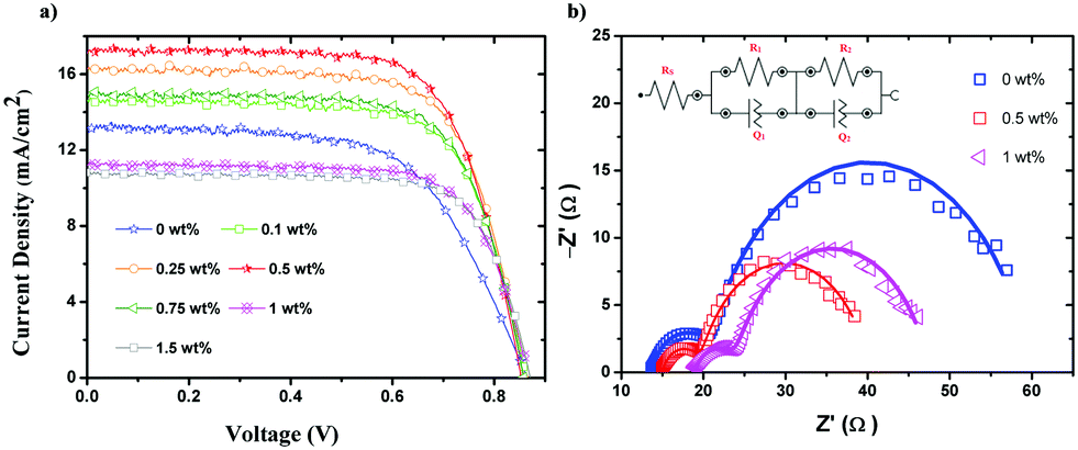 | ||
| Fig. 3 (a) J–V plots of DSSCs having different contents of CNMs in their photoanodes and (b) Nyquist plot obtained at 1 sun condition at Voc for the photoanodes loaded with 0, 0.5 and 1 wt% of CNMs (solid lines are the fit to the data). | ||
Table 1 shows the different parameters calculated from the J–V characteristics including the Jsc, Voc, FF (fill factor), and PCE. With a loading of up to 0.5 wt%, the PCE increased, beyond which it decreased, probably due to light absorption inhibited by excessive CNMs in the photoanode. The PCE of photoanode without CNMs was 7.01%, which increased to 10.24% for the photoanode loaded with 0.5 wt% of CNMs (almost 46% of enhancement in PCE upon the incorporation of CNMs). The decrease in the PCE and Jsc with a higher loading of CNMs may be due to the over-accumulation of CNMs on the TiO2 surface, promoting back-electron transfer. There was no apparent variation in the Voc and FF measured for the various loadings of CNMs, and the PCE was mostly maintained with Jsc controlled, which is dependent on the electron injection ability of the dye into the CB of TiO2 and the charge collection efficiency of TiO2. Table S4 (ESI†) shows a comparison of the literature reports on CNM-based DSSCs. To the best of our knowledge, we did not find any work incorporating size-controlled CNMs to enhance the PCE of DSSCs.
| CNMs (wt%) | J sc (mA cm−2) | V oc (V) | FF | η (%) | Avg. η for 3 cells (%) |
|---|---|---|---|---|---|
| 0 | 13.10 | 0.864 | 0.61 | 7.01 | 7.01 |
| 0.1 | 14.56 | 0.860 | 0.70 | 8.84 | 8.25 |
| 0.25 | 16.23 | 0.858 | 0.70 | 9.85 | 9.74 |
| 0.5 | 17.18 | 0.852 | 0.69 | 10.24 | 10.15 |
| 0.75 | 14.94 | 0.858 | 0.70 | 8.90 | 8.53 |
| 1 | 11.24 | 0.858 | 0.72 | 7.01 | 6.98 |
| 1.5 | 10.82 | 0.873 | 0.72 | 6.87 | 6.55 |
Electrochemical impedance analysis
The Nyquist plot shows two semicircles, where the one in the high-frequency region corresponds to the charge transfer at the counter electrode/electrolyte interface. The second semicircle in the mid-frequency region is due to the photoanode/electrolyte interface. The equivalent circuit chosen to fit the data is shown in the inset of Fig. 3b, which is Rs(R1Q1)(R2Q2), where Rs, R1, and R2 are the solution-cum-contact resistance and charge transfer resistance at the counter electrode/electrolyte and photoanode/electrolyte interfaces, respectively. Q1 and Q2 are the constant phase element associated with R1 and R2, respectively. Table S5 (ESI†) summarizes all the passive elements estimated through the fitting for the CNM loadings of 0, 0.5 and 1 wt%. Rs increased with an increase in the CNM loading since they modified the TiO2 film, resulting in contact resistance with FTO. R1, the charge transfer resistance across the counter electrode–electrolyte interface, was 7, 4.8 and 5.2 W for the CNM loading of 0, 0.5 and 1 wt%, respectively. Considering the large error in the assumption (Y1) associated with Q1, which is a constant phase element associated with R1, for practical purposes, we can assume that R1 is nearly the same. In contrast, R2, which is measured across photoanode/electrolyte interface, significantly decreased from 39.0 to 20.5 W when the CNM loading was enhanced from 0 to 0.5 wt% and 23.46 W when the loading was increased to 1 wt%. Since these values were measured at one sun condition and Voc applying 10 mV of sinusoidal AC perturbation, the equilibrium concentration of electrons in the CB of TiO2 is a function of exciton recombination, and back electron transfer to the oxidized dye, making the net current across the photoanode/electrolyte interface zero. The applied alternative current perturbation modulates the current across the photoanode/electrolyte interface, which captures the charge transfer resistance associated with the electron transfer from the photoanode to I3− in the electrolyte and/or electron transfer from I− to the oxidized dye in the photoanode. In our study, we observed a decrease in R2 and an increase in PCE at a loading of 0.5 wt% CNMs compared to the CNM-free photoanode. Therefore, the reduction in R2 is due to the effective dye regeneration by I− in the electrolyte.As observed from HR-SEM analysis, the size and amount of pores produced due to the degassing of CNMs were optimum at the CNM loading of 0.5 wt%, making it easier for the electrolyte to access the oxidized dyes present in the pores of the TiO2 layer. The pores produced by the CNMs were bigger than the inherent pore size of the TiO2 film; therefore, the incorporation of CNMs is concluded to create a hierarchical pore structure, improving the performance of the DSSCs.
Conclusions
CNMs in the size range of 1.5 to 3.5 nm were incorporated with the mesoporous TiO2 semiconductor in the photoanode of a DSSC. To the best of our knowledge, this is the first report using size-selected CNMs in the photoanode of a DSSC. The SEM analysis demonstrated the formation of wide pores and cracks in the photoanode upon the incorporation of CNMs. These pores may be beneficial for the free flow of the electrolyte into the photoanode, reducing the overpotential related to the regeneration of the oxidized dye. This could be the reason for the improved Jsc observed. For the optimized 0.5 wt% CNM-loaded photoanode, the Jsc increased from 13.10 mA cm−2 to 17.18 mA cm−2.Conflicts of interest
There are no conflicts to declare.Acknowledgements
M. A. J. acknowledges SERB for the TARE project (Ref.: TAR/2018/00048, Dt: 18.02.2019). M. A. J. also acknowledges SAIF and Department of Chemistry, IIT Madras for analytical measurements. V. S. thanks to the Department of Chemistry and BSACIST for the Senior Research Fellowship. J. S. thanks for fellowship received through SERB-N-PDF (PDF/2016/002201) and DST/TMD/SERI/HUB/1(C). Authors acknowledge the funding through DST/TMD/SERI/HUB/1(C) for establishing DSEHC (DST-IITM solar energy harnessing center). M. A. J. acknowledges Mr Ganapathirao Kandregula, research student of Prof. KR group for the assistance in impedance fitting. M. A. J. also acknowledges to Department of Metallurgical and Materials Engineering for Titan 80-300 TEM facility.References
- N. Kannan and D. Vakeesan, Renewable Sustainable Energy Rev., 2016, 62, 1092 CrossRef.
- K. Fan, J. Yu and W. Ho, Mater. Horiz., 2017, 4, 319–344 RSC.
- Q. Zheng, H. Kang, J. Yun, J. Lee, J. H. Park and S. Baik, ACS Nano, 2011, 5, 5088–5093 CrossRef CAS.
- C.-J. Lin, W.-Y. Yu and S.-H. Chien, J. Mater. Chem., 2010, 20, 1073–1077 RSC.
- Y. J. Kim, M. H. Lee, H. J. Kim, G. Lim, Y. S. Choi, N.-G. Park, K. Kim and W. Lee, Adv. Mater., 2009, 21, 3668–3673 CrossRef CAS.
- Y.-C. Park, Y.-J. Chang, B.-G. Kum, E.-H. Kong, J. Y. Son, Y. S. Kwon, T. Park and H. M. Jang, J. Mater. Chem., 2011, 21, 9582–9586 RSC.
- J. Lin, Y.-U. Heo, A. Nattestad, Y. Yamauchi, S. X. Dou and J. H. Kim, Electrochim. Acta, 2015, 153, 393–398 CrossRef CAS.
- Y. Li, H. Wang, Q. Feng, G. Zhou and Z.-S. Wang, Energy Environ. Sci., 2013, 6, 2156–2165 RSC.
- X. Dang, J. Qi, M. T. Klug, P. Y. Chen, D. S. Yun, N. X. Fang, P. T. Hammond and A. M. Belcher, Nano Lett., 2013, 13, 637–642 CrossRef CAS.
- H. Choi, W. T. Chen and P. V. Kamat, ACS Nano, 2012, 6, 4418–4427 CrossRef CAS.
- N. Yang, J. Zhai, D. Wang, Y. Chen and L. Jiang, ACS Nano, 2010, 4, 887–894 CrossRef CAS.
- L. Chen, Y. Zhou, W. Tu, Z. Li, C. Bao, H. Dai, T. Yu, J. Liuand and Z. Zou, Nanoscale, 2013, 5, 3481–3485 RSC.
- T. Ma, M. Akiyama, E. Abe and I. Imai, Nano Lett., 2005, 5, 2543–2547 CrossRef CAS.
- K. Mahmood and S. B. Park, J. Mater. Chem. A, 2013, 1, 4826–4835 RSC.
- H. Tao, W. Chen, J. Wang, W. Ke, J. Wan, J. Wu and G. Fang, Electrochim. Acta, 2014, 137, 17–25 CrossRef CAS.
- A. K. Chandiran, M. K. Nazeeruddin and M. Grätzel, Adv. Funct. Mater., 2014, 24, 1615–1623 CrossRef CAS.
- H. Elbohy, A. Thapa, P. Poudel, N. Adhikary, S. Venkatesan and Q. Qiao, Nano Energy, 2015, 13, 368–375 CrossRef CAS.
- S.-W. Lee, K.-S. Ahn, K. Zhu, N. R. Neale and A. J. Frank, J. Phys. Chem. C, 2012, 116, 21285–21290 CrossRef CAS.
- A. Lamberti, A. Sacco, S. Bianco, D. Manfredi, F. Cappelluti, S. Hernandez, M. Quaglio and C. Pirri, Phys. Chem. Chem. Phys., 2013, 15, 2596–2602 RSC.
- Y. Li, Z. Liu, C. Liu, J. Ya, W. Zhao, Q. Chen and J. Bai, J. Am. Ceram. Soc., 2012, 95, 1343–1347 CrossRef CAS.
- Z. Liu, Y. Li, C. Liu, J. Ya, W. Zhao, D. Zhao and L. An, ACS Appl. Mater. Interfaces, 2011, 3, 1721–1725 CrossRef CAS.
- Z. Liu, Y. Li, C. Liu, J. Ya, W. Zhao, E. Lei, D. Zhao and L. An, Solid State Sci., 2011, 13, 1354–1359 CrossRef CAS.
- L.-L. Li, C.-Y. Tsai, H.-P. Wu, C.-C. Chen and E. W.-G. Diau, J. Mater. Chem., 2010, 20, 2753–2758 RSC.
- W.-Q. Wu, Y.-F. Xu, C.-Y. Su and D.-B. Kuang, Energy Environ. Sci., 2014, 7, 644–649 RSC.
- F. Sauvage, D. Chen, P. Comte, F. Huang, L.-P. Heiniger, Y.-B. Cheng, R. A. Caruso and M. Graetzel, ACS Nano, 2010, 4, 4420–4425 CrossRef CAS.
- X. Tao, P. Ruan, X. Zhang, H. Sun and X. Zhou, Nanoscale, 2015, 7, 3539–3547 RSC.
- X. Li, J. Yu and M. Jaroniec, Chem. Soc. Rev., 2016, 45, 2603–2636 RSC.
- H.-Y. Chen, D.-B. Kuang and C.-Y. Su, J. Mater. Chem., 2012, 22, 15475–15489 RSC.
- Q. Zhang and G. Cao, J. Mater. Chem., 2011, 21, 6769–6774 RSC.
- S. D. Standridge, G. C. Schatz and J. T. Hupp, J. Am. Chem. Soc., 2009, 131, 8407–8409 CrossRef CAS.
- V. D. Dao, P. Kim, S. Baek, L. L. Larina, K. Yong, R. Ryoo, S. H. Ko and H. S. Choi, Carbon, 2016, 96, 139–144 CrossRef CAS.
- S. Kushwaha, S. Mandal, S. Subramanian, S. Aryasomayajul and K. Ramanujam, ChemistrySelect, 2016, 1, 6179–6187 CrossRef CAS.
- S. Paulo, E. Palomaresand and E. M. Ferrero, Nanomaterials, 2016, 6, 157–176 CrossRef.
- S. Thulasi, A. Kathiravan and M. Asha Jhonsi, ACS Omega, 2020, 5, 7025–7031 CrossRef CAS.
- W. Youfu and H. Aiguo, J. Mater. Chem. C, 2014, 2, 6921–6939 RSC.
- Z. Xiang, X. Zhou, G. Wan, G. Zhang and D. Cao, ACS Sustainable Chem. Eng., 2014, 5, 1234–1240 CrossRef.
- N. Yand, J. Zhai, D. Wang, Y. Chen and L. Jiang, ACS Nano, 2010, 4, 887–894 CrossRef.
- G. Cheng, M. S. Akhtar, O. B. Yang and F. J. Stadler, ACS Appl. Mater. Interfaces, 2013, 5(14), 6635–6642 CrossRef CAS.
- L. Chen, Y. Zhou, W. Tu, Z. Li, C. Bao, H. Dai, T. Yu, J. Liuac and Z. Zou, Nanoscale, 2013, 5, 3481 RSC.
- X. Yan, X. Cui, B. Li and L. S. Li, Nano Lett., 2010, 10, 1869–1873 CrossRef CAS.
- S. Paulo, E. Palomares and E. M. Ferrero, Nanomaterials, 2016, 6(9), 157 CrossRef.
- X. ang, T. Ma, G. Guan, M. Akiyama, T. Kida and E. Abe, J. Electroanal. Chem., 2004, 570, 257–263 CrossRef.
- S. Dong, X. Yuqing, Z. Weimin, Z. Hongtao, Z. Ying, Q. Xiting, M. Yanfeng, Y. Yong and C. Yongsheng, J. Power Sources, 2018, 384, 328–333 CrossRef.
- J.-Y. Liao, J.-W. He, H. Xu, D.-B. Kuang and C.-Y. Su, J. Mater. Chem., 2012, 22, 7910–7918 RSC.
- V. Srinivasan, M. Asha Jhonsi, M. Kathiresan and A. Kathiravan, ACS Omega, 2018, 3, 9096–9104 CrossRef CAS.
- X. Fang, M. Li, K. Guo, J. Li, M. P. Lihua, B. M. Luoshan and X. Z. Zhao, Electrochim. Acta, 2014, 137, 634–638 CrossRef CAS.
- L. Chen, Y. Zhou, W. Tu, Z. Li, C. Bao, H. Dai, T. Yu, J. Liuac and Z. Zou, Nanoscale, 2013, 5, 3481–3485 RSC.
- K. A. S. Fernando, S. Sahu, Y. Liu, W. K. Lewis, E. A. Guliants, A. Jafariyan, P. Wang, C. E. Bunker and Y.-P. Sun, ACS Appl. Mater. Interfaces, 2015, 7, 8363–8376 CrossRef CAS.
Footnotes |
| † Electronic supplementary information (ESI) available: Characterization of nanomaterial and other spectral data. See DOI: 10.1039/d0ma00654h |
| ‡ All the authors have equally contributed to this work, Dr KR facilitated writing the manuscript. |
| This journal is © The Royal Society of Chemistry 2020 |