
 Open Access Article
 This Open Access Article is licensed under a Creative Commons Attribution-Non Commercial 3.0 Unported Licence
Effect of high energy proton irradiation on MAPbI3 films for space applications observed by micro-Raman spectroscopy†
Walter O.
Herrera Martínez
ab,
Paula
Giudici
ab,
Natalia B.
Correa Guerrero
ab,
M. Luján
Ibarra
a and
M. Dolores
Perez
 *ab
*ab
aDepartamento Energía Solar, GIyA, Centro Atómico Constituyentes, CNEA, Av. Gral. Paz 1499, (1650) San Martín, Buenos Aires, Argentina. E-mail: mdperez@tandar.cnea.gov.ar
bInstituto de Nanociencia y Nanotecnología, CNEA-CONICET, Av. Gral. Paz 1499, (1650) San Martín, Buenos Aires, Argentina
First published on 17th August 2020
Abstract
Irradiation of samples with 10 MeV protons is a standard test for simulation of the outer space environment in order to qualify devices and materials for space applications. Micro-Raman spectroscopy allows one to determine the irradiation effect on methylammonium lead iodide (MAPbI3) thin films under ambient conditions and encapsulated. For the unprotected films, the vibrational modes matched previously reported lead oxide phonon frequencies and the appearance of superficial oxides was confirmed by EDAXS analysis. However, the Raman shifts corresponding to PbO were not observed for the irradiated encapsulated samples, indicating that oxidation occurs after surface exposure to ambient oxygen. Similar effects have been observed by photooxidation where the highly reactive superoxide radical is involved in the oxidation mechanism. We propose that irradiation promotes excitation of the electron cloud, which readily reduces the surface adsorbed oxygen, and this later bonds to the accessible Pb atoms.
1 Introduction
The characteristic optoelectronic properties, potential low cost and the ease of fabrication make lead halide perovskites a promising material for a wide range of electronic applications, like humidity sensors,1 lasers,2,3 3D arrays for image sensors,4 and solar cells.5,6 In particular, the use of lead halide perovskites in photovoltaic devices has received a large amount of attention due to the high conversion efficiencies achieved in only a few years. Different properties of perovskite films have been studied at length, which include thermodynamic properties,7 the effects of solvent processing,8 degradation mechanisms,9 and ionic diffusion,10 just to name a few. These efforts have helped to understand the characteristics of this novel material, allowing researchers to fabricate perovskite solar cells with power conversion efficiencies of up to 25%.11Outer space is a hostile environment for semiconductor materials; for many years researchers have studied radiation damage of Si photovoltaics and, most recently, of III–V solar cells for space applications, in order to understand the deterioration of the electronic properties and defect formation.12,13 Hybrid metal halide perovskite materials present properties, like high optical density, long carrier diffusion length,14,15 small carrier recombination times and a high tolerance to defects,5 that make them ideal candidates for solar cells and particularly interesting for space applications.16 While radiation can cause defects in typical semiconductors used in solar cells, generating losses in Jsc (short-circuit current) and Voc (open-circuit voltage), lead halide perovskite solar cells are not strongly affected by 50 keV protons as shown by Miyazawa et al.17 Even for high energy proton irradiation of 68 MeV and fluence higher than 1012 p cm−2, perovskite solar cells have been shown to exhibit negligible performance degradation.18
While lead halide perovskites are hybrid crystalline materials with interesting chemical and physical properties, they are also very sensitive to moisture, light and moderate temperatures, and so their characterization must be performed carefully in order to not modify the synthesized structures. Micro-Raman spectroscopy has proven to be a powerful technique to determine defects in different materials like SiC,19,20 III–V semiconductors (like InAs and GaAs),21 graphene22 and two dimensional semimetals.23 Some Raman studies on lead halide perovskites have been carried out recently that have allowed the analysis of organic–inorganic interactions and their crystalline phases.24–27 These studies have shown many effects, like structural changes correlated with local moisture that induce degradation of the film,26 torsional vibrations related to different degrees of order in material domains, gradual spectral changes associated with new photoinduced structure possibly caused by rearrangement of the inorganic Pb-I scaffold or structural response to ion motion.28
In this work we report the characterization by micro-Raman spectroscopy of CH3NH3PbI3 (methylammonium lead iodide, MAPbI3) thin films after sample irradiation with 10 MeV protons and 1011 p cm−2 fluence. The irradiation conditions are typically used to simulate irradiation inside the inner Van Allen belt in low-earth orbit (LEO). LEO is the most commonly used orbit for most satellites except for communication satellites that move in geostationary orbit.13 We report the vibrational modes of films under exposure to radiation while being careful not to produce degradation by the Raman laser intensity and demonstrate the inherent material resistance to permanent irradiation defect formation.
2 Experimental method
Glass substrates were cleaned with aqueous detergent solution under ultrasound for 10 min and later successively submerged in acetone and a 1![[thin space (1/6-em)]](https://www.rsc.org/images/entities/char_2009.gif) :1 mixture of ethanol and isopropyl alcohol for further washing. The substrates were later dried under a nitrogen (99.998%) flow and finally cleaned with microwave plasma.
:1 mixture of ethanol and isopropyl alcohol for further washing. The substrates were later dried under a nitrogen (99.998%) flow and finally cleaned with microwave plasma.
Highly crystalline perovskite thin films of ∼320 nm measured by SEM were obtained by a one-step method, according to the previously reported recipe using PbI2:CH3NH3I:DMSO in a 1:1:1 stoichiometric relation.29 Briefly, lead iodide (99.995%, Beantown Chemical) was completely dissolved in a solution mixture of dimethyl sulfoxide (DMSO) and dimethylformamide (DMF) (Merck), and heated at 70–80 °C. CH3NH3I (methylammonium iodide, MAI) (>99%, Greatcell Solar) was added to the resulting solution after cooling. The solution was then filtered through a PVDF syringe filter (0.45 μm pores) and spin-coated onto a glass substrate at 4000 rpm for 50 seconds. Chlorobenzene was added during spin coating as an antisolvent to enhance the crystallinity. Encapsulation by PMMA was done by spin-coating (10 mg mL−1) the solution onto the perovskite films at 4000 rpm for 30 s.
The radiation exposure of the samples was performed using a tandem type accelerator at CNEA (Tandar). The radiation beam consisted of 10 MeV proton energy and 1 × 10¹¹ p cm−2 fluence. The beam intensity was calibrated using an array of Faraday cups at the back-end of the irradiation chamber. The calibration Faraday cup current was measured with a Keithley 6514 electrometer. The perovskite films, both encapsulated and not encapsulated, are introduced into the irradiation chamber with half of the surface film exposed and the other half protected from radiation with thick glass, in order to have a control MAPbI3 film that has undergone the same experimental conditions but has not suffered irradiation.
The Raman characterization was performed in backscattering configuration with a LabRAM HR UV-vis-NIR-Horiba Jobin Yvon spectrometer with a 2.5 cm−1 spectral resolution. The setup was equipped with two excitation sources of 514 nm (Ar+ laser) and 633 nm (He–Ne laser). The Raman spectra were recorded with an integration time of 60 s using a 50× objective (3 μm spot on the sample) and a laser power between 0.03 and 1 mW.
Field Emission-Scanning Electron Microscopy (FE-SEM) images were obtained with a ZEISS LEO 982 GEMINI field emission electron microscope in secondary electron mode, using an in-lens detector to improve the resolution (CMA, Facultad de Ciencias Exactas y Naturales, UBA). X-ray diffraction measurements were performed using Empyrean PANanalytical equipment with a Cu Kα monochromatic radiation source and PIXcel 3D ultrafast detector, scanning from 10° to 60° (2θ) in 0.02 steps.
3 Results and discussion
Highly crystalline MAPbI3 perovskite thin films were prepared and selectively irradiated under simulated space radiation conditions for a typical LEO mission. The topography of both films was observed by scanning electron microscopy, SEM. Fig. 1 shows both the irradiated and non-irradiated surfaces for different magnifications. An extent of surface reconstruction with shrinking grains that conglomerate in certain areas can be observed for the MAPbI3 surface after irradiation. The close-up images reveal that after irradiation some grains remain with similar size and shape (∼100 nm) but others seem to break up into many smaller ones with different crystalline order and grouped in specific regions. | ||
| Fig. 1 SEM images for MAPbI3 films as-prepared (a and c) and after irradiation (b and d). | ||
The Raman spectra of the perovskite MAPbI3 films were obtained for both the irradiated and non-irradiated materials. The Raman shifts are significantly different for both films, as can be observed in Fig. 2. Both spectra were obtained using a very low intensity laser (P < 25 W cm−2) in order to minimize degradation effects due to the local heating by the Raman laser.26,28,30
 | ||
| Fig. 2 Raman spectra of irradiated (red) and non-irradiated (black) MAPbI3 thin films. | ||
The as-prepared film measured under environmental conditions shows a Raman spectrum that is similar to the previously reported literature.30 Contrarily, the irradiated film shows bands at 143, 284 and 337 cm−1 that have not been reported previously for MAPbI3 films with low power density measurements.26 The Raman shifts obtained for the irradiated samples are, however, very similar to previously reported PbO films. The band at 143 cm−1 can be assigned to the A1g vibrational mode, resulting from the motion of the lead atoms parallel to the c-axis in a PbO structure.31 PbO formation could account for the surface grain reconstruction observed in the SEM images. It is unfathomable that the oxide may be caused exclusively by proton irradiation since there is no oxygen atom within the MAPbI3 chemical formula. Evidently, it cannot simply be an irradiation defect but it must be coupled to exposure of the irradiated material to an oxygen source.
The formation of PbO from methylammonium lead iodide films has been described in recent work in degradation induced by light.32,33 In particular, the reports that suggest the mechanisms of oxide formation by means of extensive first-principles calculations propose that excess photogenerated electrons in MAPbI3 react with ambient molecular O2 to create the highly reactive superoxide ion (O2−). As opposed to molecular oxygen, the superoxide ion has a relatively higher bonding energy to the MAPbI3 surface, both to the Pb–I terminated and the MAI terminated (001) surfaces. Ouyang et al. and Zhang et al. suggest that physisorption is rapidly followed by chemisorption, whereas the physisorbed O2 will not form a chemical bond.34,35 Chemisorption by formation of a Pb–O bond occurs either by replacing an iodine atom that volatizes as I2, or by displacing two hydrogen atoms from the methylammonium that consequently form H2O leaving behind the Pb–O bond. In this work, under normal experimental conditions, we do not observe PbO formation by photodegradation since the non-irradiated sample (that underwent the same experimental conditions as the irradiated sample) presents a Raman spectrum corresponding to neat perovskite samples as reported previously. Contrarily, the proton irradiated samples show extensive lead oxide formation. In this case, we propose that the superoxide ion is formed by the interaction of excess electrons promoted in the perovskite film by the 10 MeV proton radiation. At this energy, protons are 105 times more likely to interact with the electron cloud than with the structural nucleus, thus causing a density of high energy and highly reactive electrons. The resulting highly reactive surface reduces atmospheric oxygen to form superoxide ions that later physisorb and chemisorb to the perovskite surface. The proposed reaction mechanism is as follows:
| MAPbI3 + 10 MeV radiation → MAPbI3 (e−)* | (1) |
| MAPbI3 (e−)* + O2 → MAPbI3 + O2− → MAPbI3: O2− (physisorbed) | (2) |
| MAPbI3: O2− (physisorbed) → MAI + PbO + I2 | (3) |
It is not clear whether oxygen incorporation occurs inside the irradiation chamber or after the sample is extracted and exposed to ambient air. Even though the oxygen concentration in a vacuum chamber is very low, it could be enough to react with the highly reactive excess electrons on the MAPbI3 surface.
Superoxide formation must occur faster than the MAPbI3 (e−)* decay rate to the ground state. Further studies to evaluate the lifetime of the perovskite excited state after irradiation should be carried out by time resolved experiments coupled to the particle accelerator experimental line in order to determine the relevance of the oxygen concentration to the mechanism second step. However, we believe it is unlikely that the MAPbI3 (e−)* state would live long enough before the chamber can be opened safely after irradiation (2–3 hours).
The Raman spectrogram for PbO films has been thoroughly studied in previous work by Wiechert et al.31 In that report, the α- and β-PbO polymorphs present specific intensity ratios for the 284 and 335 nm signal. For ratios I(284)/I(335) > 1, the predominant phase is the orthorrombic β-PbO phase, while the α-phase is predominant when the ratio is inversed. Both the tetragonal α-PbO and the orthorrombic β-PbO phases can be observed for the irradiated samples in different regions of the sample, with ratios varying from 1.46 to 0.84 for Fig. 3, top and bottom, respectively.
 | ||
| Fig. 3 Raman spectra for irradiated MAPbI3 films in different regions of the film sample. | ||
A simple method to confirm that the PbO polymorph formation is originated by the convolution of the proton irradiation and later exposure to atmospheric oxygen is by encapsulating the surface with PMMA. PMMA is transparent to radiation due to the very small thickness and it efficiently protects the surface from atmospheric oxygen. Fig. 4 shows the Raman spectra for both irradiated MAPbI3 samples with and without PMMA encapsulation. The unprotected surface shows the typical PbO Raman shift at 140 cm−1 as observed in Fig. 2. Contrarily, the encapsulated sample does not present significant oxidation into PbO as the Raman spectra do not present the corresponding PbO shifts. We propose that the excited electron cloud caused by irradiation will recombine and reversibly relax to the ground state if no oxidative compound meets the interface. It must be mentioned that the Raman spectrum for the encapsulated sample does not exactly match the neat perovskite spectra presented in Fig. 2 but instead it is similar to the spectrum of barely degraded perovskite film by Raman laser local heating.26,30 The presence of the PMMA top layer demands to use a more intense laser in order to achieve a significant signal. If extremely low power is used, no signal is observed, and therefore we increased the power intensity during the measurement until a good enough signal-to-noise ratio was achieved, causing some perovskite degradation by the Raman laser as reported elsewhere in the literature.26,28 The Raman degradation spectra for our perovskite films were measured and presented in the ESI;† no PbO shifts are observed when the film is degraded by the Raman laser with time or by increasing the laser intensity. It can be positively affirmed that proton irradiation does not provoke any permanent defects in the perovskite semiconductor material as opposed to other inorganic semiconductors applied to solar cells like Si, CIGS, III–V, etc. This result is in agreement with published literature demonstrating the radiation hardness of perovskite solar cells,17,18 where the electronic excitation by irradiation may not provoke oxidation of the adjacent layers (TiO2 and spiro-OMeTAD, typically) and the film quickly relaxes to its ground state.
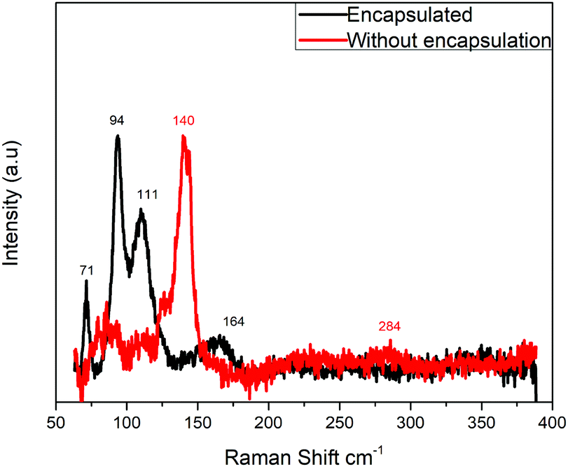 | ||
| Fig. 4 Raman spectra of irradiated MAPbI3 thin films encapsulated with PMMA and without encapsulation. | ||
The presence of the different atomic elements in the film was evaluated by EDAXS. Table 1 shows the representative sample elements and the percentual difference between the non-irradiated and the irradiated sample, unencapsulated. We observe a clear reduction of the atomic % of Pb and I due to an increase of the O percent for the irradiated samples vs. the as-prepared films. Additionally, the MAPbI3 stoichiometric 3:1 iodine to lead ratio is observed, suggesting that the perovskite crystal still remains as the majority material. A silicon signal is also present as it is part of the glass substrate material (SiO2). It could be argued that an increase of the oxygen signal would correspond to substrate exposure upon irradiation by formation of holes and craters; however, the Si amount is almost constant for both samples while the oxygen increase is significant for the irradiated samples. The SEM images presented in Fig. 1 also show no apparent substrate exposure.
| Element | Non-irradiated MAPbI3 | Irradiated MAPbI3 | % Difference |
|---|---|---|---|
| Atomic % | Atomic % | ||
| O | 19.36 | 22.48 | +16.12 |
| Si | 14.64 | 14.97 | +2.25 |
| I | 5.96 | 5.30 | −11.07 |
| Pb | 1.94 | 1.76 | −9.28 |
Further evaluation of the irradiated material was observed by XRD and photoluminescence spectroscopy (PL). The grazing angle X-ray diffraction pattern does not show an appreciable difference for both irradiated and non-irradiated films. The diffractograms are presented in Fig. 5 and show the typical tetragonal MAPbI3 phase. There are no observable PbI2 or PbO features from degradation/oxidation either by humidity or by irradiation. The PL emission signal of the MAPbI3 film also remains mostly unaffected after irradiation (see the ESI†).
 | ||
| Fig. 5 Grazing angle X-ray diffraction patterns for the fresh and irradiated perovskite film. | ||
The absence of a PbO signal in the X-ray diffraction pattern for the irradiated sample seems to confirm that the bulk perovskite remains unaffected and PbO is only formed as a thin top surface layer that cannot be detected by the DRX technique. As the superoxide reacts with the surface perovskite, it forms a coating film that prevents further reaction from happening as the O2− ions can no longer access the deeper MAPbI3 layer. This passivation effect has been reported earlier for the photodegradation mechanism34 and it is then plausible that in our experiment only a thin top layer of PbO is obtained. During the Raman measurement, the top PbO film may likely absorb the normal incident laser beam, shielding not only the laser from reaching the bottom bulk perovskite but also preventing its weak signal response from being observed.
4 Conclusions
Hybrid organo-lead halide perovskite solar cells reportedly show excellent properties under irradiation for space applications. We investigated the effect of proton irradiation on MAPbI3 films by Raman measurements and confirmed the perovskite hardness to radiation. The irradiated samples do not present any new signal in the Raman spectra that could be assigned to a non-reversible chemical change or defect formation. Conversely, when the films are exposed to an ambient atmosphere after irradiation, the Raman signal reveals the formation of PbO. The incorporation of oxygen into the perovskite structure is assumed to follow the same mechanism as photooxidation: the excited electron cloud caused by collisions of high energy protons promotes superoxide formation, which readily oxidizes the MAPbI3 top surface into PbO. The oxide formation results in a thin top layer that passivates the bulk perovskite and prevents further oxidation. The presence of superficial oxide on the irradiated film exposed to an ambient atmosphere was confirmed by EDAXS, whereas the GI-XRD measurement does not reveal any PbO signal, and only the crystallographic planes from the neat perovskite can be observed. These observations are consistent with the presence of a top thin PbO layer: a very weak Raman signal from the perovskite (screened by the PbO layer), a strong PbO Raman signal and an X-ray diffractogram showing only the bulk halide perovskite. We can further conclude that the MAPbI3 material is inert to high energy proton irradiation as long as it does not come in contact with an oxidizing substance; this is relevant in terms of designing the device architecture when it is subjected to irradiation so that the perovskite layer is not only isolated from atmospheric oxygen but is also in contact with layers that will not promote an oxidized interface. In this regard, a study of the radiation effect of devices under different hole transporting materials (HTMs) is underway in order to evaluate the MAPbI3/HTM interface for possible oxidation under irradiation.Conflicts of interest
There are no conflicts to declare.Acknowledgements
The authors are thankful for financial support from Consejo Nacional de Investigaciones Científicas y Tecnológicas (CONICET, PIP 0808CO), Agencia Nacional de Promoción Científica y Tecnológica (ANPCyT, PICT 2015-1961) and Fundación Innovación y Tecnología (FUNINTEC, INTERING 2016). The authors are indebted to Martín Alurralde (DES-CNEA) for the use of the irradiation line, E. B. Halac (DMC-CNEA) for Raman measurements and to M. C. Marchi (CMA-UBA) for the SEM measurements. WOHW and NCG thank CONICET for their doctoral scholarship. MDP and PG are staff members of CONICET.Notes and references
- K. Ren, L. Huang, S. Yue, S. Lu, K. Liu, M. Azam, Z. Z. Wang, Z. Wei, S. Qu and Z. Z. Wang, J. Mater. Chem. C, 2017, 5, 2504–2508 RSC.
- H. Zhu, Y. Fu, F. Meng, X. Wu, Z. Gong, Q. Ding, M. V. Gustafsson, M. T. Trinh, S. Jin and X.-Y. Zhu, Nat. Mater., 2015, 14, 636–642 CrossRef CAS.
- Y. Jia, R. A. Kerner, A. J. Grede, A. N. Brigeman, B. P. Rand and N. C. Giebink, Nano Lett., 2016, 16(7), 4624–4629 CrossRef CAS.
- L. Gu, M. M. Tavakoli, D. Zhang, Q. Zhang, A. Waleed, Y. Xiao, K. Tsui, Y. Lin, L. Liao, J. Wang and Z. Fan, Adv. Mater., 2016, 28(44), 9713–9721 CrossRef CAS.
- J. P. Correa-Baena, A. Abate, M. Saliba, W. Tress, T. Jesper Jacobsson, M. Grätzel and A. Hagfeldt, Energy Environ. Sci., 2017, 10, 710–727 RSC.
- T. Duong, J. Peng, D. Walter, J. Xiang, H. Shen, D. Chugh, M. N. Lockrey, D. Zhong, J. Li, K. J. Weber, T. P. White and K. R. Catchpole, ACS Energy Lett., 2018, 3(10), 2441–2448 CrossRef CAS.
- G. P. Nagabhushana, R. Shivaramaiah and A. Navrotsky, Proc. Natl. Acad. Sci. U. S. A., 2016, 113, 7717–7721 CrossRef CAS.
- N. J. Jeon, J. H. Noh, Y. C. Kim, W. S. Yang, S. Ryu and S. Il. Seok, Nat. Mater., 2014, 13, 897–903 CrossRef CAS.
- J. Bisquert and E. J. Juarez-perez, J. Phys. Chem. Lett., 2019, 10, 5889–5891 CrossRef CAS.
- W. Peng, C. Aranda, O. M. Bakr, G. Garcia-Belmonte, J. Bisquert and A. Guerrero, ACS Energy Lett., 2018, 3(7), 1477–1481 CrossRef CAS.
- J. Duan, H. Xu, W. E. I. Sha, Y. Zhao, Y. Wang, X. Yang and Q. Tang, J. Mater. Chem. A, 2019, 7, 21036–21068 RSC.
- M. Alurralde, M. J. L. Tamasi, C. J. Bruno, M. G. Marťnez Bogado, J. Plá, J. Fernández Vázquez, J. Durán, J. Schuff, A. A. Burlon, P. Stoliar and A. J. Kreiner, Sol. Energy Mater. Sol. Cells, 2004, 82, 531–542 CAS.
- M. Ochoa, E. Yaccuzzi, P. Espinet-González, M. Barrera, E. Barrigón, M. L. Ibarra, Y. Contreras, J. García, E. López, M. Alurralde, C. Algora, E. Godfrin, I. Rey-Stolle and J. Plá, Sol. Energy Mater. Sol. Cells, 2017, 159, 576–582 CrossRef CAS.
- D. Shi, V. Adinolfi, R. Comin, M. Yuan, E. Alarousu, A. Buin, Y. Chen, S. Hoogland, A. Rothenberger, K. Katsiev, Y. Losovyj, X. Zhang, P. A. Dowben, O. F. Mohammed, E. H. Sargent and O. M. Bakr.
- Y. Tian and I. G. Scheblykin, J. Phys. Chem. Lett., 2015, 6, 3466–3470 CrossRef CAS.
- Y. Miyazawa, M. Ikegami, H.-W. Chen, T. Ohshima, M. Imaizumi, K. Hirose and T. Miyasaka, iScience, 2018, 2, 148–155 CrossRef CAS.
- Y. Miyazawa, M. Ikegami, T. Miyasaka, T. Ohshima, M. Imaizumi and K. Hirose, 2015 IEEE 42nd Photovolt. Spec. Conf. PVSC 2015, 2015, 4–7.
- N. H. Nickel, F. Lang, V. V. Brus, J. Bundesmann, S. Seidel, A. Denker, S. Albrecht, G. Landi and H. C. Neitzert, in Physics, Simulation, and Photonic Engineering of Photovoltaic Devices VII, ed. A. Freundlich, L. Lombez and M. Sugiyama, SPIE, 2018, vol. 10527 Search PubMed.
- G. Litrico, N. Piluso and F. La Via, Mater. Sci. Forum, 2017, 897, 303–306 Search PubMed.
- S. Nakashima, Y. Nakatake, Y. Ishida, T. Talkahashi and H. Okumura, Phys. B, 2001, 310, 684–686 CrossRef.
- R. Tanta, C. Lindberg, S. Lehmann, J. Bolinsson, M. R. Carro-temboury, K. A. Dick, T. Vosch, T. S. Jespersen and J. Nygård, Phys. Rev. B, 2017, 96(16), 165433–165440 CrossRef.
- A. Eckmann, A. Felten, I. Verzhbitskiy, R. Davey and C. Casiraghi, Nano Lett., 2012, 12(8), 3925–3930 CrossRef CAS.
- H. Yuan, X. Zhou, Y. Cao, Q. Bian, Z. Zhang, H. Sun, S. Li, Z. Shao and J. Hu, npj 2D Mater. Appl., 2019, 3, 12 CrossRef.
- L. Q. Xie, T. Y. Zhang, L. Chen, N. Guo, Y. Wang, G. K. Liu, J. R. Wang, J. Z. Zhou, J. W. Yan, Y. X. Zhao, B. W. Mao and Z. Q. Tian, Phys. Chem. Chem. Phys., 2016, 18, 18112–18118 RSC.
- C. Quarti, G. Grancini, E. Mosconi, P. Bruno, J. M. Ball, M. M. Lee, H. J. Snaith, A. Petrozza and F. De Angelis, J. Phys. Chem. Lett., 2014, 5, 279–284 CrossRef CAS.
- M. Ledinský, P. Löper, B. Niesen, J. Holovský, S. J. Moon, J. H. Yum, S. De Wolf, A. Fejfar and C. Ballif, J. Phys. Chem. Lett., 2015, 6, 401–406 CrossRef.
- B. W. Park, S. M. Jain, X. Zhang, A. Hagfeldt, G. Boschloo and T. Edvinsson, ACS Nano, 2015, 9, 2088–2101 CrossRef CAS.
- R. Gottesman, L. Gouda, B. S. Kalanoor, E. Haltzi, S. Tirosh, E. Rosh-Hodesh, Y. Tischler, A. Zaban, C. Quarti, E. Mosconi and F. De Angelis, J. Phys. Chem. Lett., 2015, 6, 2332–2338 CrossRef CAS.
- C. Aranda, C. Cristobal, L. Shooshtari, C. Li, S. Huettner and A. Guerrero, Sustain. Energy Fuels, 2017, 1, 540–547 RSC.
- P. Pistor, A. Ruiz, A. Cabot and V. Izquierdo-roca, Nat. Publ. Gr, 2016, 1–8 Search PubMed.
- D. U. Wiechert, S. P. Grabowski and M. Simon, Thin Solid Films, 2005, 484, 73–82 CrossRef CAS.
- N. Aristidou, C. Eames, I. Sanchez-Molina, X. Bu, J. Kosco, M. S. Islam and S. A. Haque, Nat. Commun., 2017, 8, 15218 CrossRef.
- W. Kong, A. Rahimi-Iman, G. Bi, X. Dai and H. Wu, J. Phys. Chem. C, 2016, 120(14), 7606–7611 CrossRef CAS.
- Y. Ouyang, Y. Li, P. Zhu, Q. Li, Y. Gao, J. Tong and L. Shi, J. Mater. Chem. A, 2019, 7, 2275–2282 RSC.
- L. Zhang and P. H.-L. Sit, J. Mater. Chem. A, 2017, 5(19), 9042–9049 RSC.
Footnote |
| † Electronic supplementary information (ESI) available. See DOI: 10.1039/d0ma00583e |
| This journal is © The Royal Society of Chemistry 2020 |