
 Open Access Article
 This Open Access Article is licensed under a Creative Commons Attribution-Non Commercial 3.0 Unported Licence
Enhancement in performance of ternary blend-polymer solar cells using a PEDOT:PSS–graphene oxide hole transport layer via Förster resonance energy transfer and balanced charge transport†
Lalsingh
Guguloth
a,
Kuldeep
Singh
 b,
V. S. Reddy
Channu
c and
Kusum
Kumari
*a
b,
V. S. Reddy
Channu
c and
Kusum
Kumari
*a
aDepartment of Physics, National Institute of Technology, Warangal-506004, Telangana, India. E-mail: kusum@nitw.ac.in
bCSIR-Central Electrochemical Research Institute, Chennai Unit, CSIR Madras Complex, Taramani, Chennai-600113, Tamilnadu, India
cSMC Corporation, College Station, Texas TX 77845, USA
First published on 21st October 2020
Abstract
In this work, we report high performance ternary blend polymer solar cells (TPSCs) fabricated by employing poly((3-hexyl)thiophene) (P3HT): poly[4,8-bis(5-(2-ethylhexyl)thiophen-2-yl)benzo[1,2-b;4,5-b′]dithiophene-2,6-diyl-alt-(4-(2-ethylhexyl)-3-fluorothieno[3,4-b]thiophene)-2-(carboxylate-2-6-diyl)] (PTB7-Th): PC71BM ternary blend as the active layer, and poly(3,4-ethylene-dioxythiophene):poly(styrenesulfonate) (PEDOT:PSS)–graphene oxide (GO) composite as the hole transport layer (HTL). The power conversion efficiency (PCE) of the best TPSC is enhanced to ∼7.1% as compared to that of P3HT:PC71BM (PCE ∼ 3.7%) and PTB7-Th:PC71BM (PCE ∼ 4%) reference binary blend based devices. The enhancement in PCE is attributed to the synergistic effect of superior photovoltaic properties of P3HT:PTB7-Th:PC71BM (0.3![[thin space (1/6-em)]](https://www.rsc.org/images/entities/char_2009.gif) :0.7:1) ternary blend as well as better hole-transport properties of PEDOT:PSS–GO (1:1) composite HTL. External quantum efficiency spectra showed a broad spectral response with photon-to-electron conversion approaching up to 67–75% in the extended wavelength range of 350–780 nm covering the Vis-NIR range, potentially due to the complementary absorption from the P3HT and PTB7-Th molecules. Photoluminescence (PL) quenching and time-resolved PL studies demonstrated a significant reduction in photo-exciton lifetime τ1 from 129 ps (in P3HT) to 17 ps (in P3HT:PTB7-Th:PC71BM), which signifies quick and strong non-radiative relaxation of the photo-excited excitons. This is primarily dominated by both Förster resonance energy transfer and charge transfer mechanisms owing to cascade energy level alignment, and subsequently lead to effective exciton dissociation in the ternary blend. Balanced hole and electron mobilities (μe/μh = 1.81) facilitate the charge transport, and is governed by the trap-free space charge limited current with weak bimolecular recombination. Also, the conductivity and ultraviolet-photoelectron measurements revealed that the addition of GO nanosheets in PEDOT:PSS imparts high electrical conductivity and increases the work function of HTL such that its HOMO level match perfectly with the HOMO level of the polymers in the active layer. This reduces the potential barrier at the HTL/active layer interface and promotes both the hole extraction and transport. Moreover, the incorporation of GO nanosheets results in increase of LUMO level of the PEDOT:PSS HTL which effectively block the electrons and facilitate the transport of holes in HTL without recombination. The simultaneous existence of all these beneficial properties of the ternary blend collectively boost the performance of TPSCs by enhancing the short-circuit current to 12.3 mA cm−2, open-circuit voltage to 0.74 V, and fill-factor to 0.78. These findings show that (P3HT:PTB7-Th:PC71BM) and PEDOT:PSS–GO composites can be the promising ternary blend active layer and hole transporting material, respectively, for achieving high performance PSCs. This work provides a new platform for the development of the ternary blend approach of PSC technology.
:0.7:1) ternary blend as well as better hole-transport properties of PEDOT:PSS–GO (1:1) composite HTL. External quantum efficiency spectra showed a broad spectral response with photon-to-electron conversion approaching up to 67–75% in the extended wavelength range of 350–780 nm covering the Vis-NIR range, potentially due to the complementary absorption from the P3HT and PTB7-Th molecules. Photoluminescence (PL) quenching and time-resolved PL studies demonstrated a significant reduction in photo-exciton lifetime τ1 from 129 ps (in P3HT) to 17 ps (in P3HT:PTB7-Th:PC71BM), which signifies quick and strong non-radiative relaxation of the photo-excited excitons. This is primarily dominated by both Förster resonance energy transfer and charge transfer mechanisms owing to cascade energy level alignment, and subsequently lead to effective exciton dissociation in the ternary blend. Balanced hole and electron mobilities (μe/μh = 1.81) facilitate the charge transport, and is governed by the trap-free space charge limited current with weak bimolecular recombination. Also, the conductivity and ultraviolet-photoelectron measurements revealed that the addition of GO nanosheets in PEDOT:PSS imparts high electrical conductivity and increases the work function of HTL such that its HOMO level match perfectly with the HOMO level of the polymers in the active layer. This reduces the potential barrier at the HTL/active layer interface and promotes both the hole extraction and transport. Moreover, the incorporation of GO nanosheets results in increase of LUMO level of the PEDOT:PSS HTL which effectively block the electrons and facilitate the transport of holes in HTL without recombination. The simultaneous existence of all these beneficial properties of the ternary blend collectively boost the performance of TPSCs by enhancing the short-circuit current to 12.3 mA cm−2, open-circuit voltage to 0.74 V, and fill-factor to 0.78. These findings show that (P3HT:PTB7-Th:PC71BM) and PEDOT:PSS–GO composites can be the promising ternary blend active layer and hole transporting material, respectively, for achieving high performance PSCs. This work provides a new platform for the development of the ternary blend approach of PSC technology.
Introduction
Single junction bulk-heterojunction (BHJ) polymer solar cells (PSCs) based on a binary blend of donor and acceptor have proved to be a promising photovoltaic technology in the extensive research of the past few decades.1–6 Their use is emerging as a novel approach owing to their low cost, light weight, flexibility, easy processing, and tunable electrical and optical properties.7–10 Such binary blends composed of conjugated polymers such as poly((3-hexyl)thiophene) (P3HT),4 poly[N-9′-heptadecanyl-2,7-carbazole-alt-5,5-(4′,7′-di-2-thienyl-2′,1′,3′-benzothiadiazole)] (PCDTBT),10 poly[2,6-(4,4-bis(2-ethylhexyl)-4H-cyclopenta[2,1-b;3,4-b′]dithiophene)-alt-4,7(2,1,3-benzothiadiazole)] (PCPDTBT),11 poly[(ethylhexyloxy)-benzodithiophene-(ethylhexyl)-thienothiophene] (PTB7),12,13 poly[4,8-bis(5-(2-ethylhexyl)thiophen-2-yl)benzo[1,2-b;4,5-b′]dithiophene-2,6-diyl-alt-(4-(2-ethylhexyl)-3-fluorothieno[3,4-b]thiophene)-2-(carboxylate-2-6-diyl)] (PBDTTT-EFT or PTB7-Th),13 poly[(4,8-bis-(2-ethylhexyloxy)-benzo(1,2-b:4,5-b′)dithiophene)-2,6-diyl-alt-(4-(2-ethylhexanoyl)-thieno[(3,4-b]thiophene)-2-6-diyl)] (PBDTTT-C),14 and poly[(5,6-dihydro-5-octyl-4,6-dioxo-4H-thieno[3,4-c]pyrrole-1,3-diyl)[4,8-bis[(2-ethylhexyl)oxy]benzo[1,2-b:4,5-b′]dithiophene-2,6-diyl]] (PBDTTPD)10 as electron donors, and [6,6]-phenyl C71-butyric acid methyl ester (PC71BM) and indene-C60 bisadduct (ICBA) as electron acceptors, demonstrated the state-of-the-art PCEs approaching ∼15–17%.6–9 Unfortunately, these binary blends exhibit poor solar light harvesting, due to the intrinsically narrow absorption bands of most of these polymer donors, and weak absorption of the PCBM acceptor (only in the UV region), wasting a significant fraction of available solar light.15–17 However, their poor stability is also a matter of concern. To address all these issues, more recently, a new morphological strategy of using ternary blends has been adopted by adding a third ternary component into the binary blend, which could either be a donor or an acceptor, resulting in (D1:D2:A) and (D:A1:A2) ternary systems, respectively.18–20 This technology, popularly known as ternary blend solar cells (TPSCs), has drawn great interest as they not only provide an advantage of strong light harvesting by complementary absorption, but also effectively improve charge generation and carrier collection properties.15–25 Many reports on ternary blends describe an enhanced exciton dissociation probability as supported by Förster resonance energy transfer (FRET) between donor–donor, and charge transfer (CT) at the donor/acceptor interface due to cascade energy alignment, in different ternary blend systems.20,25,26 Besides, a suitable microstructure, solution-processing, and easy fabrication are some of the added advantages over the widely used tandem solar cell technology.20–26 Currently, TPSCs have PCEs exceeding 12%.19–25 Nevertheless, for improving the performance of TPSCs, it is mandatory to control the blend morphology, and optimize the photovoltaic processes such as exciton generation, dissociation, carrier generation, charge transport, and collection. However, understanding the underlying mechanisms is not straightforward and requires extensive studies. Detailed and in-depth studies on the morphology, photo charge carrier dynamics, charge carrier transport (trap-limited and recombination-limited), etc. of the ternary system are very limited.Furthermore, it has been reported by several groups that the hole transport layer (HTL) plays another crucial role in deciding the device performance. Poly(3,4-ethylene dioxythiophene):poly(styrenesulfonate) (PEDOT:PSS), the most popularly used HTL, suffers from degradation problems due to high hygroscopic and high acidic nature; and also exhibit poor electrical conductivity.26–29 This results in poor device stability and also deteriorates the device efficiency. As an alternative, MoO3 and V2O5 are used to overcome the problem of photostability.26–29 However, high-cost vacuum deposition techniques and incompatibility with solution-processing and roll-to-roll processing make these materials less viable. Therefore, the development of easy-to-process, cost-effective, and highly stable HTLs with good hole transport capabilities are urgently demanded. Keeping this in view, 2D materials such as graphene oxide (GO) have been reported as efficient HTLs, showing encouragingly good performances when used in PSCs.30,31 GO is known to possess good optical and electronic properties, high electron and hole mobilities, good thermal and chemical stability, and easy to synthesize, making it an ideal candidate to facilitate charge transport more effectively and impart long-term stability. Nevertheless, the cell performance becomes greatly sensitive to film thickness because of its non-connecting channels and insulating nature. As an alternative, several reports are also available on incorporating GO nanosheets into PEDOT:PSS to overcome the challenges and proved PEDOT:PSS–GO composites to be the promising HTL exhibiting beneficial hole transport properties.29,32–35 Motivated by this, we adopted a PEDOT:PSS–GO composite HTL for the development of TPSCs. The uniqueness of this work is that we have used a stable ternary blend system and the HTL with GO to develop highly stable TPSCs with reasonably high efficiency keeping in view their commercial viability.
Here, we fabricated TPSCs using a ternary blend of dual donors, P3HT (high band-gap) and PTB7-Th (low band-gap), and the organic acceptor PC71BM as the active layer, and employing the PEDOT:PSS–GO (1:1) composite as the HTL. Low temperature, low cost, and solution-based easy processing have been adopted for the fabrication of these TPSCs. For understanding explicitly the behavior of the ternary blend and the role of the PEDOT:PSS–GO composite HTL, it is worth mentioning that in BHJs, the photovoltaic conversion involves five major steps: (1) solar light-absorption and exciton-generation; (2) exciton diffusion to the donor/acceptor interface; (3) exciton-dissociation leading either to the formation of the charge-transfer (CT) complex or further dissociation into free charge carriers; (4) carrier transport, via the hopping mechanism without and via trap assisted recombination processes; (5) carrier collection at the respective electrodes.26 Each of these steps becomes a bottleneck that could limit the solar photovoltaic conversion. Herein, we present the optimization of all these steps focusing both on the active layer of (P3HT:PTB7-Th:PCBM) ternary blend and the PEDOT:PSS–GO (1:1) HTL. Firstly, the influence of the third additive, i.e. PTB7-Th, in the ternary blend has been investigated thoroughly in three different compositions of PTB7-Th in P3HT, and the properties of the ternary blend active layer are optimized. Secondly, the effect of GO in PEDOT:PSS has also been studied in detail for the optimization of hole transport properties. Finally, the photo-exciton lifetime, carrier dissociation, charge extraction, charge transport properties, and carrier recombination dynamics of the fabricated TPSCs have been measured and studied systematically. We report that TPSCs employing the P3HT:PTB7-Th:PC71BM (0.3:0.7:1) ternary blend and the PEDOT:PSS–GO (1:1) composite HTL show a PCE of ∼ 7.1%, which is an enhancement of 48% and 45% compared to the P3HT:PC71BM (PCE ∼ 3.7%) and PTB7-Th:PC71BM (PCE ∼ 4%) binary BHJ solar cells, respectively. This is primarily due to an increase in short circuit current (Jsc) to 12.3 mA cm−2, open circuit voltage (Voc) to 0.74 V, and fill factor (FF) to 0.78 in the case of the ternary solar cells. When compared with the TPSC device having only PEDOT:PSS HTL, an enhancement of 55% in PCE has been observed in PEDOT:PSS–GO composite HTL based devices. Besides, these devices showed long-term photostability. We present a detailed analysis and a closer look at the underlying photovoltaic processes and corresponding prevailing mechanisms accounting for the improvement in the performance of the TPSCs. We found that the improvement in the performance of the P3HT:PTB7-Th:PC71BM (0.3:0.7:1) ternary blend based TPSC devices with the PEDOT:PSS–GO (1:1) composite HTL is attributed to the (i) broad spectral coverage of solar light harvesting owing to strong and complementary absorption; (ii) efficient exciton dissociation into free charge carriers via FRET and CT at the D1/D2 and D/A interfaces; (iii) high charge extraction ability at the HTL/active layer interface due to the well-matched HOMO level of PEDOT:PSS–GO with the HOMO of the polymer donors; (iv) balanced carrier transport and suppressed bimolecular recombination in the ternary blend and (v) the efficient electron blocking capability of PEDOT:PSS–GO, which reduces the probability of HTL/active layer interface state induced-recombination losses, facilitating carrier collection. This work unveils the device physics that is fundamentally important for the design and development of more stable and efficient TPSCs.
Results and discussion
A schematic representation of the device configuration of TPSCs fabricated with a conventional device architecture using a dual donor and acceptor, i.e. (D1:D2:A) type of ternary blend composed of P3HT (D1), PTB7-Th (D2) and PCBM acceptor (A), is shown in Fig. 1(a). The chemical structure of the respective donor, acceptor materials, PEDOT:PSS and GO is also been shown in Fig. 1(b).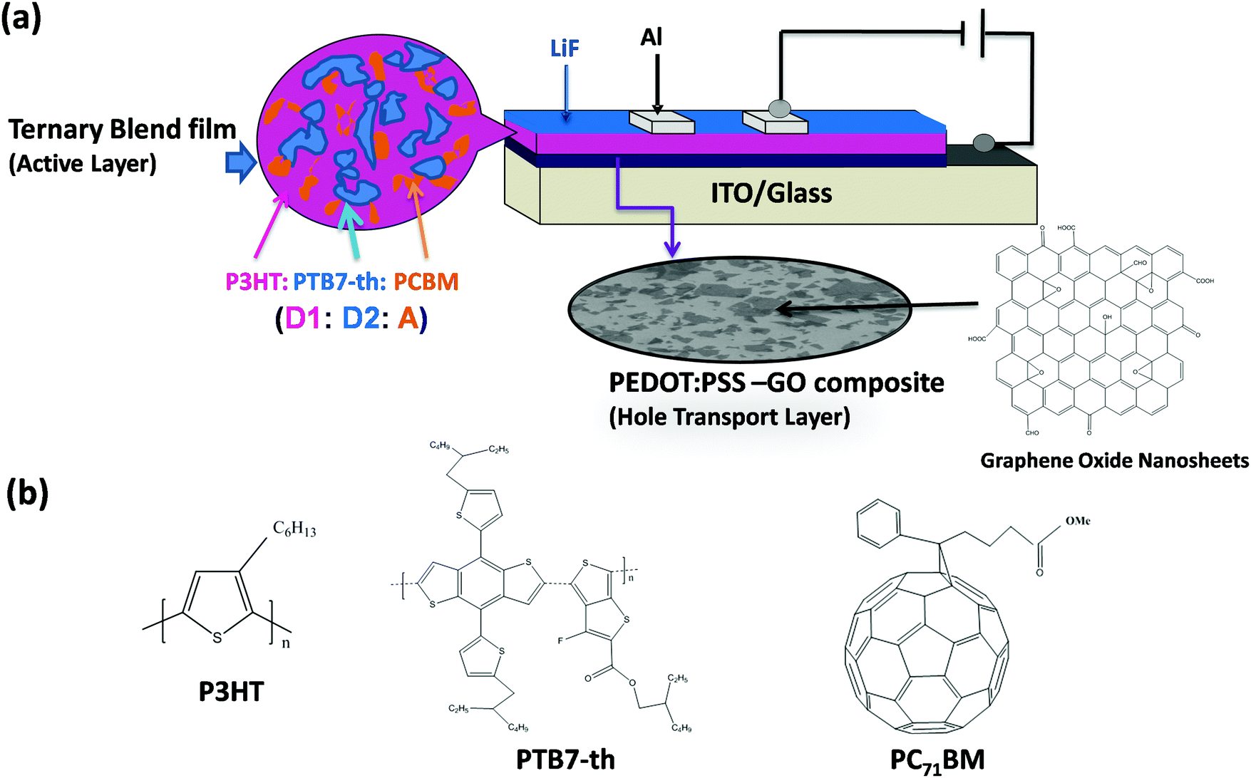 | ||
| Fig. 1 (a) Schematic of the device configuration of TPSCs using the ternary blend (P3HT:PTB7-Th:PCBM) and employing the PEDOT:PSS–GO composite (1:1) HTL. (b) Chemical structure of polymer donors, P3HT and PTB7-Th, and the organic acceptor, PC71BM. | ||
For TPSCs, the ternary blend active layer and the PEDOT:PSS–GO composite HTL have been optimized individually in terms of their optical and electronic properties to achieve efficient photovoltaic properties.
Structural, optical and electrical properties of GO, PEDOT:PSS and PEDOT:PSS–GO HTLs
To investigate the potential of PEDOT:PSS–GO in TPSCs as the HTL, we first evaluated the elementary structural, optical and electronic properties via X-ray diffraction (XRD), field emission scanning electron spectroscopy (FESEM), atomic force microscopy (AFM), optical transmittance, UV-Vis absorption, Raman spectroscopy, and four-point probe conductivity measurements, respectively, and subsequently studied the effect of the incorporation of GO nanosheets into PEDOT:PSS on the device performances of the TPSCs.Fig. S1(a and b) in the ESI† show FESEM and AFM images of GO nanosheets deposited on the ITO substrate, respectively, revealing that the size of GO nanosheets, synthesized using the modified Hummer's method (described in the Experimental section), is in the range of 5–10 μm. The height of the white line scan in the AFM image of a single GO nanosheet on the ITO substrate, as shown in the inset, is ∼1.1 nm, which is consistent with the thickness of single GO nanosheets reported elsewhere.29,30 PEDOT:PSS–GO composite films were deposited by dispersing GO in PEDOT:PSS with a weight ratio of 1:1. Fig. S1(c and d) (ESI†) depict the FESEM and AFM images of PEDOT:PSS–GO composite films deposited on ITO, showing that GO is dispersed homogeneously in the PEDOT:PSS matrix, with a low surface RMS = 1.21 nm.33
Fig. S2(a) in the ESI† shows the XRD patterns of GO, PEDOT:PSS and PEDOT:PSS:GO composite films; the GO sample shows a single peak at 11.3° corresponding to the (001) lattice plane, which is the characteristic peak, as reported elsewhere.33,38 The Raman spectra of GO, as shown in Fig. S2(b) (ESI†), display two dominant peaks at 1340 and 1604 cm−1, associated with the D and G bands, respectively.38 The G band is attributed to the Csp2–Csp2 stretching mode in the basal plane of the GO sheets, and the D band corresponds to the degree of functionalization and becomes active in the presence of defects in the graphene structure. The higher the intensity of the D band, the greater the number of structural defects. This means that the ID/IG ratio can be used to measure the degree of the presence of defects in the graphene structure.39 The origin of the defects could be the breaking of a single bond, double bond, or both in the basal plane of the graphene structure. Also, attached oxygen-containing functional groups like hydroxyl, carbonyl, carboxyl and carboxylate groups, etc. to graphene are considered as defects.39 Here, the ID/IG ratio is 1.06, which is consistent with other reported work.39
As solar light is incident from the anode side, the optical transmittance capability of the anodes and hole transport layers plays a primary role on the performance of TPSC devices, and therefore, it is an important parameter. The transmittance spectra of GO, PEDOT:PSS and PEDOT:PSS–GO (1:1) composite films in the visible range (see Fig. S3 in the ESI†) demonstrate that the GO nanosheets have relatively high transmittance in the entire visible range of 300–800 nm as compared to pure PEDOT:PSS films. Also, the incorporation of GO nanosheets in PEDOT:PSS in a 1:1 ratio drastically increases the transmittance of the PEDOT:PSS–GO composite films to almost 92% at the 550 nm wavelength, which is much higher than the value 84% observed for PEDOT:PSS and 89% observed for GO. This property makes the PEDOT:PSS–GO (1:1) composite is beneficial for TPSC devices as a HTL.38
Further investigation of the UV-Vis absorption spectra, we calculated the energy bandgap (Eg) from the Tauc plots for GO, PEDOT:PSS, PEDOT:PSS–GO (1:1) composite films [shown in Fig. S4(a–d), ESI†] using the formula αhν = (hν − Eg)1/2, where α is the absorption coefficient and hν is the photon energy. Here, we estimated that Eg = 3.61 eV for GO, Eg = 1.71 eV for PEDOT:PSS, and Eg = 3.39 eV for PEDOT:PSS–GO(1:1) films. Also, the work function (Φ), HOMO level (EHOMO) and LUMO level (ELUMO) of all these HTL films were calculated via ultraviolet photoelectron spectroscopy (UPS) using the formulas Φ = hν − (Ecutoff − EF), EHOMO = Φ + (EHOMOedge − EF), and ELUMO = EHOMO − Eg, where hν is excitation energy (21.2 eV) and Ecutoff − EF is the binding energy at the secondary electron cutoff. The parameters obtained from the UPS spectra of PEDOT:PSS, GO, and PEDOT:PSS–GO samples, shown in Fig. S5 (ESI†), are mentioned in Table S1 (ESI†). The EHOMO values for PEDOT:PSS and PEDOT:PSS–GO (1:1) were determined to be 5.01 eV and 5.22 eV. Interestingly, the work function increased from 4.8 eV to 5.0 eV on adding GO into PEDOT:PSS in a 1:1 composition. This increase in work function originates from the benzoid–quinoid transition of the PEDOT:PSS structure caused by the oxygen functional groups breaking the sp2 π–π conjugation bond, as previously reported by Jae Choul Yu et al.32 The increase of Φ and EHOMO of PEDOT:PSS–GO makes the HOMO of the HTL match perfectly well with the HOMO of the polymer donors, as represented in the schematic of energy level alignment of PEDOT:PSS/GO/PEDOT:PSS–GO (1:1) HTLs along with the P3HT:PTB7-Th:PCBM ternary blend shown in Fig. 2. Therefore, in TPSCs, this will result in efficient hole extraction properties at the HTL/active layer interface because of the almost zero potential barrier at the interface.
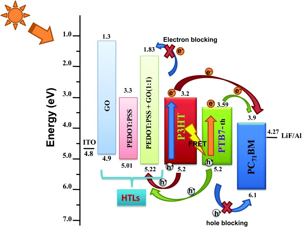 | ||
| Fig. 2 Energy level diagram of P3HT:PTB7-Th:PCBM TPSCs along with PEDOT:PSS/GO/PEDOT:PSS–GO (1:1) HTLs. | ||
To investigate this influence of GO on the sheet resistance and the conductivity of PEDOT:PSS, we estimated the sheet resistance (Rsheet) and electrical conductivity (σ) of pure PEDOT:PSS, GO, and the PEDOT:PSS–GO (1:1) composite film through four-point probe measurements. The dispersion of GO in PEDOT:PSS lowers the Rsheet from 221 Ω □−1 (for pure PEDOT:PSS) to 59 Ω □−1 obtained for PEDOT:PSS–GO (1:1). And, there is a significant increase in conductivity σ = 4 × 10⁻³ S cm−1 (for PEDOT:PSS) to 16.9 × 10⁻³ S cm−1. This is apparently due to the availability of a large number of C–C sp2 hybridized sigma bonds in the basal plane of each GO nanosheet imparting more conductivity. It is, thus, justified that PEDOT:PSS–GO (1:1) possesses extremely good charge transport capability and could prove to be a good HTL.
Solar absorption and photo-excited carrier dynamics of the ternary blend
The ternary blend of P3HT:PTB7-Th:PCBM has been investigated in different blend compositions for optimizing the photovoltaic properties. The P3HT:PTB7-Th films were deposited on ITO by mixing P3HT and PTB7-Th in three different weight proportions, i.e., (0.7:0.3), (0.5:0.5) and (0.3:0.7) weight ratios. The recorded absorption spectra, depicted in Fig. 3, confirmed that all three P3HT:PTB7-Th films with (0.7:0.3), (0.5:0.5), and (0.3:0.7) exhibit strong and complementary absorption covering a wide wavelength range of 500–750 nm. This widening of the absorption window is due to the contribution of both P3HT in the 480–640 nm region, and PTB7-Th in the 650–750 nm region of the solar spectrum. Evidently, P3HT:PTB7-Th with a (0.3:0.7) weight ratio displays stronger and wider coverage in the entire solar light spectrum as compared to the other two compositions.
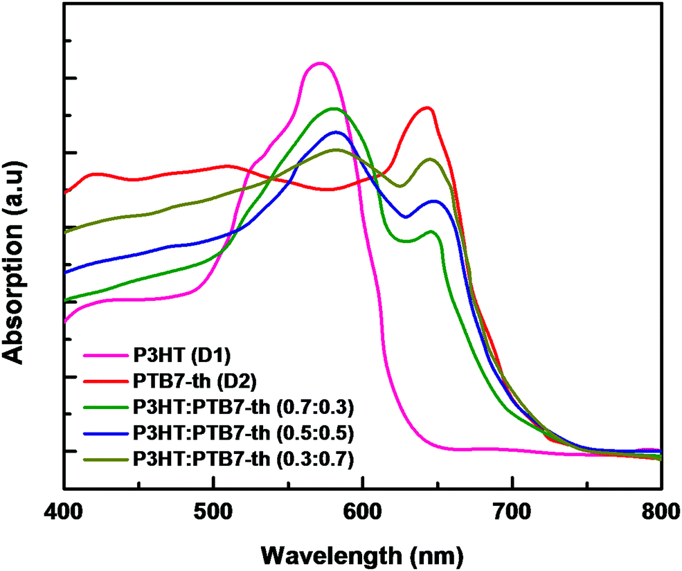 | ||
| Fig. 3 Absorption spectra of P3HT (D1) and PTB7-Th (D2), and P3HT:PTB7-Th showing complementary absorption. | ||
Furthermore, it is noteworthy that these ternary blend systems [(D1:D2:A)/(D:A1:A2)] offer cascade energy alignment depending on the HOMO and LUMO energy levels of the respective donors and acceptors these systems are composed of. Depending on their respective band-gaps, the formation of three different cascade structures are reported in the literature. A schematic representation of three different types of cascade structures particularly for (D1:D2:A) ternary blends are presented in Fig. 4. The possible exciton dissociation mechanisms via FRET between the two donors and CT at donor/acceptor interfaces are governed by the type of cascade formation.16,23 As can be seen in Fig. 4(a–c), the first category is the A-type [D1:D2(low Eg):A] blend system wherein both FRET and CT are possible. The B-type [D1:D2(low Eg):A] blend also represents the same yet with different energy alignment. However, the third category, the C-type [D1:D2(high Eg):A] blend system, demonstrates only CT with no possibility of FRET.16,40 So far, all these three categories of cascade ternary blends, reported worldwide for TPSCs, achieved a noticeable increase in PCEs up to 30–50% owing to sensitized emission, and strong PL quenching due to FRET/charge transfer assisted enhanced exciton dissociation within the ternary blend.16,27 However, very few reports are available on the dynamics of exciton dissociation in these (D1:D2:A) systems and its effect on device performance. Particularly, the P3HT:PTB7-Th:PCBM blend, which falls under the A-type of ternary systems,23 is a new ternary blend combination with only a few reports available till now, and detailed studies focusing on the device physics and the excited state carrier dynamics are rare. We aim at revealing precisely the same in the ternary blend of (P3HT:PTB7-Th:PCBM). Here, in this A-type ternary blend also, the cascade structure is expected to trigger both FRET and CT at donor/donor intermixed phases and donor/acceptor interfaces in the blend film (as shown in Fig. 2).
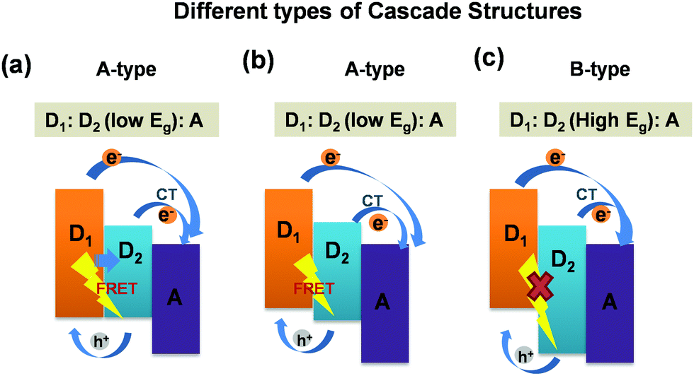 | ||
| Fig. 4 Schematic energy diagrams of different cascades of dual donor and acceptor interfaces: (a) (A-type) [D1:D2(low Eg):A] blend system: both FRET and CT processes possible; (b) (A-type) [D1:D2(low Eg):A] blend system: both FRET and CT processes possible; (c) (B-type) [D1:D2(high Eg):A] blend system: only CT possible and FRET prohibited. | ||
The probabilities of FRET and CT were investigated via studying the steady-state photoluminescence (PL) characteristics of pure P3HT, PTB7-Th, and P3HT:PTB7-Th mixed blends in different weight ratios at 465 nm excitation wavelength [Fig. 5(a)]. The two major effects observed in the PL spectra with increasing concentration of PTB7-Th in the P3HT polymer are (i) PL quenching due to a considerable decrease of characteristic PL peaks of P3HT at 650 nm (corresponding to (0–0) π*–π transition), (ii) the appearance of a PL peak at 738 nm in P3HT:PTB7-Th (0.7:0.3) films, which further shifts to 747 nm and increases in intensity, in both P3HT:PTB7-Th (0.5:0.5) and P3HT:PTB7-Th (0.3:0.7) films, respectively, indicating sensitized emission channeled towards the PTB7-Th polymer. Both this PL quenching (in P3HT) and sensitized emission (towards PTB7-Th) are due to dominating energy transfer as well as electron transfer processes from P3HT (D1) to PTB7-Th (D2).20,26,27
 | ||
| Fig. 5 (a) Steady-state PL spectra of P3HT, PTB7-Th, and P3HT:PTB7-Th:PC71BM films at the excitation wavelength of 465 nm. PL curves show sensitized PL and PL quenching in the mixed blends without and with PCBM. (b) Overlap of PL spectra of P3HT and absorption of PTB7-Th, indicating that non-radiative FRET occurs dominantly between P3HT and PTB7-Th in P3HT:PTB7-Th blends causing PL quenching. (c) TRPL decay curve corresponding to pure P3HT and dual donor P3HT:PTB7-Th blends in different compositions (without and with PCBM). (d) Fitting of PL decay curves (solid lines) using the bi-exponential and tri-exponential decay equation where τ represents the photon–exciton lifetime and the χ2 value is ∼1.1 in the numerical fitting parameter. | ||
To verify the PL quenching of the P3HT PLpeak at 650 nm via energy transfer, we checked for the overlap of the PL emission spectra of P3HT with the absorption spectra of PTB7-Th by plotting them together in Fig. 5(b). It can be seen that the absorption edge of PTB7-Th lies exactly at the PLpeak of P3HT, which satisfies the criterion for FRET occurrence. Hence, FRET will take place from one donor, i.e., P3HT, to another donor, i.e., PTB7-Th.26,27 Apparently, P3HT molecules transfer non-radiative de-excitation exciton energy to PTB7-Th via FRET. The ground state PTB7-Th molecules thereby absorb this energy and move to the excited state leading to the generation of excitons in PTB7-Th, which subsequently may or may not recombine radiatively, depending on the donor/acceptor interface it forms with the acceptor. The parameter that is important in any FRET process is the Förster radius (R0), which reveals the distance for 50% FRET efficiency, and is calculated as ∼5.7 nm, as per the equation:40,42
where FD(λ) is the normalized donor emission spectrum, and εA is the acceptor molar extinction coefficient.
Apart from FRET, another reason for PL quenching of the P3HT peak is electron transfer, which probably occurs at the P3HT/PTB7-Th interface due to the energy cascade alignment of P3HT and PTB7-Th polymer donors. Furthermore, when the PCBM acceptor is blended with the donor:donor P3HT:PTB7-Th (0.3:0.7) composite, the PL at both the characteristic peaks of P3HT (650 nm) and PTB7-Th (747 nm) gets completely quenched, as shown in Fig. 5(a). This PL quenching owing to non-radiative exciton de-excitation confirms markedly enhanced charge transfer at the donor–acceptor interface, i.e., P3HT/PCBM and PTB7-Th/PCBM interfaces, leading to efficient exciton dissociation [see Fig. 6(a)].
 | ||
| Fig. 6 (a) J–V characteristics of TPSCs (Device 1): ITO/PEDOT:PSS–GO (1:1)/P3HT:PTB7-Th:PCBM (0.3:0.7:1)/LiF/Al, under Air Mass 1.5 Solar illumination (Pin = 100 mW cm−2), and comparison with Device 2: ITO/PEDOT:PSS–GO (1:1)/P3HT:PCBM (1:1)/LiF/Al, and Device 3: ITO/PEDOT:PSS–GO (1:1)/PTB7-Th:PCBM (1:1)/LiF/Al. (b) EQE spectra of Device 1, Device 2 and Device 3. | ||
To provide evidence of FRET and CT processes, we probed the fluorescence decay dynamics in P3HT:PTB7-Th: blends without and with the PCBM ternary additive by time-resolved PL (TRPL) measurements via a time-correlated single-photon count (TCSPC) and estimated the photo-excited carrier lifetime. Fig. 5(c) exhibits the PL decay spectra of pure P3HT, and P3HT:PTB7-Th dual donor systems (three different compositions) and also with PCBM acceptor, at the excitation wavelength (λexc) of 550 nm and emission wavelength (λem) of 650 nm (PLpeak), respectively. It helps in understanding the exact origin of non-radiative fluorescence, i.e., whether PL quenching occurs via the charge transfer or by FRET. All the PL decay profiles were fitted with the well-known multi-exponential function described elsewhere [Fig. 5(d)],41–43
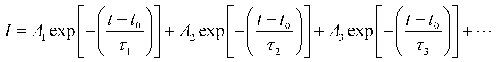
| Active layer blends | A 1 | τ 1 (ps) | A 2 | τ 2 (ps) | A 3 | τ 3 (ps) | τ avg (ps) | Efficiency of FRET EFRET = 1 − (τD–A/τD) |
|---|---|---|---|---|---|---|---|---|
| P3HT | 0.89 | 129 | 0.11 | 590 | — | — | 360 | — |
| P3HT:PTB7-Th (0.7:0.3) |
0.75 | 80 | 0.25 | 419 | — | — | 329 | E FRET = 37.9% |
| P3HT:PTB7-Th (0.5:0.5) |
0.62 | 61 | 0.38 | 315 | — | — | 188 | E FRET = 52.7% |
| P3HT:PTB7-Th (0.3:0.7) |
0.57 | 47 | 0.43 | 206 | — | — | 126 | E FRET = 63.5% |
| P3HT:PTB7-Th:PCBM (0.3:0.7:1) |
0.46 | 17 | 0.28 | 42 | 0.26 | 109 | 24 | E FRET&CT = 86.8% |
Here, a closer look into the time-resolved decay parameters reveals that the lifetimes for non-radiative and radiative transitions change individually upon the addition of PTB7-Th into P3HT in different compositions, respectively, and also when the PCBM acceptor is added into the P3HT:PTB7-Th dual donor blend. The decay of the pristine P3HT film is bi-exponential with τ1 = 129 ps (A1 = 0.89) and τ2 = 560 ps (A2 = 0.11). This indicates that 89% of the PL quenching takes place at decay time τ1 = 129 ps, while ∼11% PL intensity prevails due to radiative recombination (τ2 = 560 ps) within the existing traps in the bulk polymer and surface states at the polymer crystallite boundaries apparently due to the highly disordered conducting polymer molecular chains. The blending of donor P3HT with another donor PTB7-Th strongly quenches the P3HT PL emission, reduces the photo-exciton lifetime τ1 from 129 ps (A2 = 0.89) to 80 ps (A2 = 0.75), 61 ps (A2 = 0.62), and 47 ps (A2 = 0.57), respectively, in case of different P3HT:PTB7-Th (0.7:0.3), (0.5:0.5), and (0.3:0.7) blend compositions. This decrease in the photo-exciton lifetime in donor P3HT strongly implies that the non-radiative relaxation of these photo-excited excitons is initiated and relaxation energies are transferred to ground state donor PTB7-Th molecules by dipole–dipole interaction-based FRET, causing excitation in PTB7-Th molecules followed by a dominant radiative de-excitation process. The latter process is confirmed through the coincident increase seen in the slow A2 or longer-lived τ2 component, i.e., from 590 ps (A2 = 0.11) to 419 ps (A2 = 0.25), 315 ps (A2 = 0.38), and 206 ps (A2 = 0.43) in these respective P3HT:PTB7-Th (0.7:0.3), (0.5:0.5), and (0.3:0.7) blends, i.e., with increasing compositions of PTB7-Th in P3HT. The increased percentage of A2 amplitudes also confirms that the higher the PTB7-Th concentration in P3HT, the more prominent the FRET-governed PL quenching, and thereby, the greater generation of excitons in PTB7-Th polymer. This effect was further quantified by calculating the FRET efficiency (EFRET). The EFRET from donor P3HT to donor PTB7-Th (which acts as an energy acceptor in the present case) can be quantified by the formula: EFRET = 1 − τD–A/τD. In the formula, τD and τD–A are the PL lifetime of the excited exciton in single donor P3HT in the absence and presence of the acceptor (PTB7-Th), respectively. The EFRET in P3HT:PTB7-Th blends increases from 37.9% obtained in [P3HT:PTB7-Th (0.7:0.3)] to 52.7% and 63.5%, obtained for [P3HT:PTB7-Th (0.5:0.5)] and P3HT:PTB7-Th (0.3:0.7) blends, respectively. Furthermore, upon addition of PCBM into the P3HT:PTB7-Th (0.3:0.7) blend, the exciton lifetime further decreases drastically from τ1 = 47 ps (A1 = 0.89) to τ1 = 17 ps (A2 = 0.11), which is a direct experimental evidence of an additional charge transfer process at the donor/acceptor interface, i.e., P3HT/PCBM and PTB7-Th/PCBM interfaces in the ternary blend, besides FRET, as the cascade energy alignment favors charge separation/dissociation with the total efficiency (FRET and CT) reported to be a maximum of 86.8%. Wang et al. reported the same energy transfer and charge transfer processes simultaneously occurring among the dual donors and donor–acceptor species,42 however, dominated mainly by CT, are significant pathways to generate higher photocurrents. Also, note that the other long-lived τ2 = 42 ps and τ3 = 109 ps lifetime components can probably be attributed to the non-radiative recombination enabled by defects and impurities and bimolecular recombination.43,44 These results show that the enhanced energy and charge transfer efficiency achieved in the ternary blend may improve the overall characteristic performance of TPSCs using such a P3HT:PTB7-Th:PCBM (0.3:0.7:1) ternary blend as an active layer.
Photovoltaic performance
The TSCSs were fabricated using a ternary blend, i.e., P3HT:PTB7-Th:PCBM (0.3:0.7:1) (best composition) and the HTL of PEDOT:PSS–GO (1:1) composite films. The J–V characteristics of TPSC Device 1 [ITO/PEDOT:PSS–GO (1:1)/P3HT:PTB7-Th:PCBM (0.3:0.7:1)/LiF/Al] under Air Mass 1.5 Solar illumination are presented in Fig. 6(a), and they are compared with Device 2 [ITO/PEDOT:PSS–GO (1:1)/P3HT:PCBM (1:1)/LiF/Al] and Device 3 [ITO/PEDOT:PSS–GO (1:1)/PTB7-Th:PCBM (1:1)/LiF/Al]. The photovoltaic parameters for all the three devices are summarized in Table 2.
| Devices | Device structure | J sc (mA cm−2) | V oc (V) | FF | PCE (%) | R s (Ω cm2) | R sh (Ω cm2) |
|---|---|---|---|---|---|---|---|
| Device 1 | ITO/PEDOT:PSS + GO (1:1) HTL/P3HT:PTB7-Th:PCBM (0.3:0.7:1)/LiF/Al |
12.3 | 0.74 | 0.78 | 7.1 | 5 | 4111 |
| Device 2 | ITO/PEDOT:PSS + GO (1:1) HTL/P3HT:PCBM (1:1)/LiF/Al |
8.9 | 0.62 | 0.67 | 3.7 | 21 | 2761 |
| Device 3 | ITO/PEDOT:PSS + GO (1:1) HTL/PTB7-Th:PCBM (1:1)/LiF/Al |
9.6 | 0.71 | 0.58 | 4 | 19 | 2897 |
The performance of Device 1 with P3HT:PTB7-Th:PCBM is superior to that of the binary blend based Device 2 (P3HT:PCBM) and Device 3 (PTB7-Th:PCBM), showing a huge enhancement in PCE to ∼ 7.1% compared to PCE = 3.7% (Device 2) and PCE = 4% (Device 3). Hence, there is an increment of 45–48% in the ternary blend based device, apparently attributed to the significantly high Jsc, Voc and FF as compared to the values obtained for binary blend based Device 2 and Device 3, respectively. The improvement in Jsc is ascribed to the reduction of series resistance (Rs) to 5 Ω cm2 and increase of shunt resistance (Rsh) to 4111 Ω cm2 in Device 1, compared to Device 2 (Rs = 21 Ω cm2; Rsh = 2761 Ω cm2) and Device 3 (Rs = 19 Ω cm2; Rsh = 2897 Ω cm2) (see Table 2). On the other hand, the significant improvement in the performance of Device 1 is due to (i) high exciton generation due to strong and extended light absorption, as shown by the ternary blend (Fig. 3) and (ii) efficient exciton dissociation at the donor/acceptor interface via FRET and CT due to the cascade energy alignment of the ternary blend, as proved by TRPL studies in the ternary blend. And, this exciton dissociation at the HTL/active layer, as already discussed earlier, was further accelerated by the use of the PEDOT:PSS–GO composite HTL, due to the well-matched HOMO levels of the HTL and polymer donors.
To understand further the enhanced performance shown by Device 1, detailed and comparative investigations were performed focusing on the exciton dissociation, carrier generation, and carrier transport properties in the P3HT:PTB7-Th:PCBM (0.3:0.7:1) ternary blend.
Carrier generation, charge extraction and transport properties
In general, to get photocurrent, the bound electron–hole pair (excitons) should dissociate and generate free charge carriers, which should get collected at the respective electrodes before getting lost through recombination processes.This step-up of Jsc in the ternary blend is elucidated by the results of the EQE spectra shown in Fig. 6(b). The enhanced EQE in an overall broader wavelength range is clearly seen for the ternary blend Device 1. Also, the Jsc values calculated using EQE data were within 2% error of the Jsc values obtained in the J–V measurements. The binary devices with P3HT:PCBM (Device 2) show a narrow absorption range, however with high conversion percentages of 69% at 432 nm and 79% at 573 nm. On the other hand, PTB7-Th:PCBM based Device 3 exhibits comparatively broad spectral absorption, however, with slightly lower conversion percentages i.e., 61% at 370 nm, 56% at 432 nm, 66% at 541 nm, and maintaining the same 66% up to 674 nm. It can be seen that the TPSCs with the P3HT:PTB7-Th:PCBM ternary blend (Device 1) showed a high and broad spectral response in the wavelength range from 300 nm to 800 nm with a maximum peak approaching 65% at 400 nm and 74% at 700 nm of EQE, which is divided into two regions; a low wavelength region of 380–510 nm with 65–67%, and a high wavelength region of 540–700 nm with 73–74%. This is essentially in agreement with the absorption spectra and is attributed to the combined and complementary absorption effect from P3HT and PTB7-Th molecules. This improvement is highly beneficial for photovoltaics for achieving a high Jsc.
For efficient carrier collection, the charge transport properties of the active layer play a crucial role. It is believed that the charge transport is governed by the carrier mobilities, which are restricted by the existence of traps. The trap density describes the recombination losses in the film. Hence, it is important to examine the hole and the electron mobilities in the ternary blend device (Device 1) which showed the best performance. We analyzed the carrier mobilities, trap density, and trap depth by measuring J–V characteristics of the P3HT:PTB7-Th:PCBM ternary blend in the dark, and compared these with the P3HT:PCBM and PTB7-Th:PCBM binary blend based devices, as shown in Fig. 7(a–c).
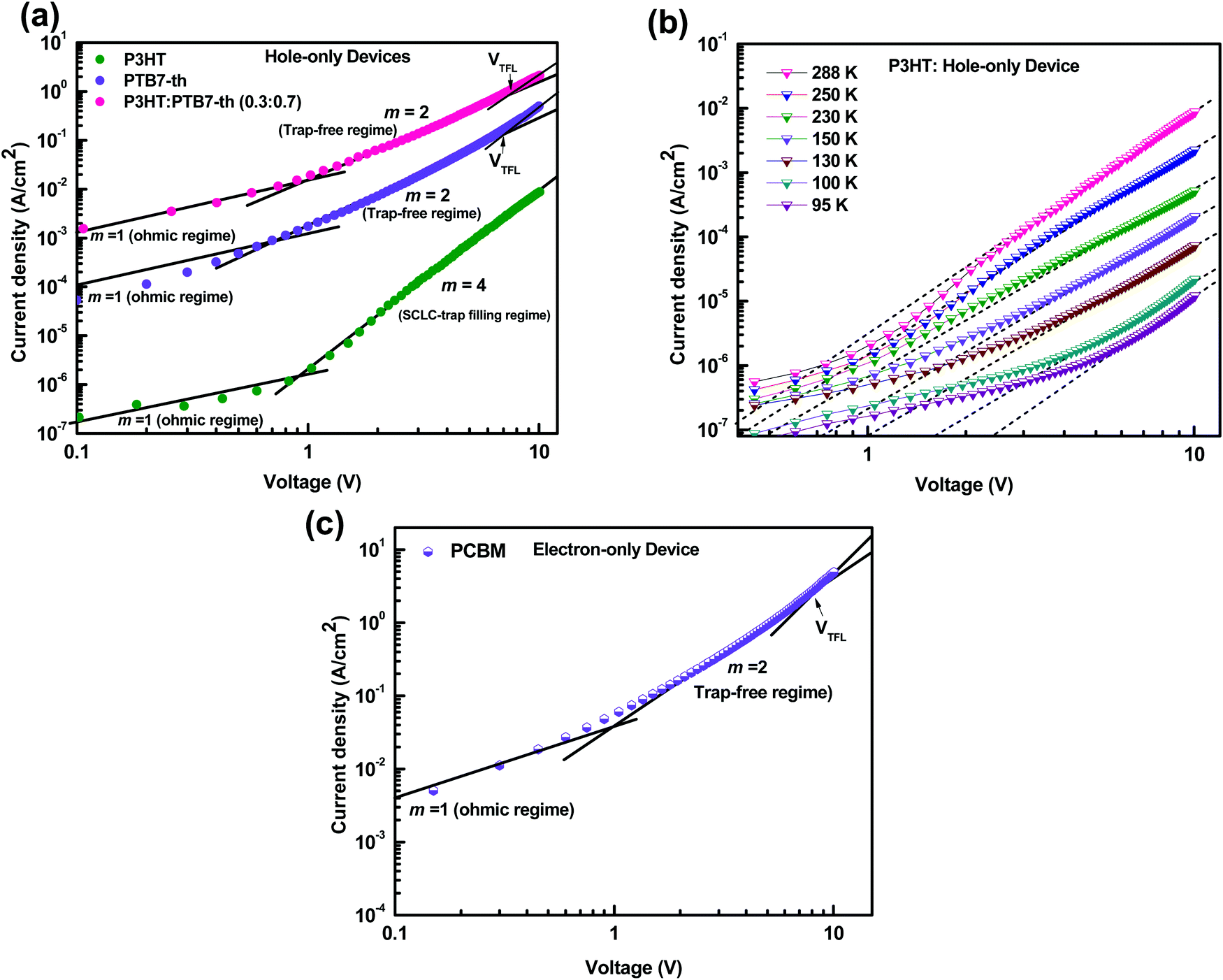 | ||
| Fig. 7 (a) J–V characteristics in the dark for P3HT, PTB7-Th, and P3HT:PTB7-Th (0.3:0.7) in the hole-only device configuration, ITO/PEDOT:PSS/polymer/Au. (b) Hole-only device: ITO/PEDOT:PSS/P3HT/Au at different temperatures, 288–95 K. (c) J–V characteristics of electron-only devices in the dark for PC71BM, ITO/PEDOT:PSS/PCBM/LiF/Al. | ||
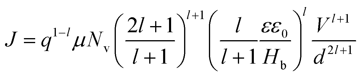
Earlier studies on organic materials have suggested that the charge transport is governed by a strong power-law dependence, J ∼ Vm, in the dark. Based on the exponent m of the J–V curve, transport could either be trap-free (m = 2) or trap-limited (m > 2).44 Furthermore, the trap-limited transport can be described due to a single discrete level of (shallow) traps or traps distributed in energy and space. In either case, if the injected carrier concentration (Pi) exceeds the background carrier concentration (Po), then the so called space charge limited current (SCLC) “Trap model” is observed.44
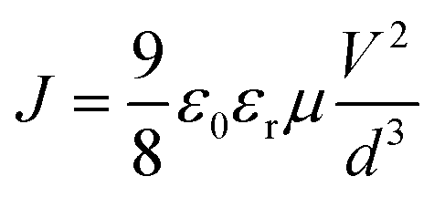
Assuming Pi < Po, charge transport follows the Mott–Gurney law,45–48
 | (1) |
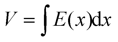
However, when Pi < Po, the continuity equation and boundary conditions are described by
| J = qμp(x)E(x) | (2) |
 | (3) |
 | (4) |
 | (5) |
Fig. 7(a) shows the J–V characteristics of hole-only devices, ITO/PEDOT:PSS/polymer film (180 nm)/Au, at room temperature. The J–V curves are displayed for P3HT, PTB7-Th, and the P3HT:PTB7-Th (0.3:0.7) blend film, respectively, for comparison of their hole charge transport properties. Herein, for the P3HT film, initially, the Ohmic regime with m = 1 is observed at low electric fields followed by the trap-filling regime at high electric fields signifying the SCLC behavior. Hence, as SCLC behavior dominates, we further measured the J–V characteristics at different temperatures in the range of 288–95 K, shown in Fig. 7(b), which have been theoretically analyzed both using the SCLC trap model assuming the exponential distribution of traps in energy and space using eqn (4) and (5), respectively. The comparison of the experimental data (symbols) with the theoretically generated curves (dashed lines) for the temperature range of 288–95 K proves that the trap model governs the J–V behavior across the temperature range. The curve fitting generated fitting parameters are Hb = 3.7 × 1018 cm−3, Nv = 1.1 × 1019 cm−3, εr = 3, ε0 = 8.85 × 10⁻¹⁴ F cm−1, μh = 5 × 10⁻⁵ cm2 V−1 s−1, d = 180 nm, and Tc = 850 K, which corresponds to Et = 95 meV.
In the J–V characteristics of the PTB7-Th film, a trap-free behavior is observed, as indicated by the m = 2 regime at high electric fields. Therefore, the curves are fitted with the Mott–Gurney Child's law, see eqn (1), resulting in μh = 8 × 10⁻⁴ cm2 V−1 s−1 using εr = 3.5 and d = 180 nm. Interestingly, in the blend of the P3HT:PTB7-Th (0.3:0.7) film, we discovered that the trap-free transport is the only dominating mechanism, wherein no SCLC trap-limited conduction is seen. The fitting reveals μh = 1.1 × 10⁻⁴ cm2 V−1 s−1 using εr = 3.35 and d = 180 nm.
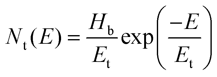
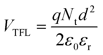
The hole trap density Nt is calculated by the equation shown below:49
 | (6) |
:0.7), hence the same effect could cause trap-free transport of carriers. The low trap densities of the traps in PTB7-Th and P3HT:PTB7-Th films result in a significant increase in hole mobility to μh = 1.1 × 10⁻⁴ cm2 V−1 s−1 and μh = 8 × 10⁻⁴ cm2 V−1 s−1, respectively, as compared to μh = 5 × 10⁻⁵ cm2 V−1 s−1 in P3HT. The enhancement in mobilities support the higher current densities observed in PTB7-Th and P3HT:PTB7-Th films.
Fig. 7(c) shows the J–V characteristics of the PC71BM thin film in the electron-only device configuration. Here, good current densities are achieved, which are dominated by a trap-free electron transport shown by the m = 2 regime at high electric fields. The fitting with Mott–Gurney Child's law, eqn (1), yields the electron mobility μe = 2 × 10⁻³ cm2 V−1 s−1 obtained by using εr = 4 and d = 180 nm. From VTFL = 8.1 V, Nt = 1.08 × 1017 cm−3 is derived.
The morphology of the active layer also plays a major role in governing the carrier transport properties. The morphology of the binary blends, P3HT:PCBM and PTB7-Th:PCBM, and the P3HT:PTB7-Th:PCBM ternary blend has been investigated via AFM, yielding RMS roughness values of 2.87 nm, 1.92 nm and 1.05 nm, respectively [shown in Fig. 8(a–c)]. This means that the blending of P3HT with PTB7-Th markedly improves the morphology by producing less aggregations and reducing the RMS roughness. This improved morphology is responsible for the reduction of Nt (as discussed above). This is consistent with the high carrier mobilities (balanced), and hence, justifies the trap-free charge transport observed in P3HT:PTB7-Th:PCBM ternary blends. This supports the enhancement in Jsc observed in TPSC devices.
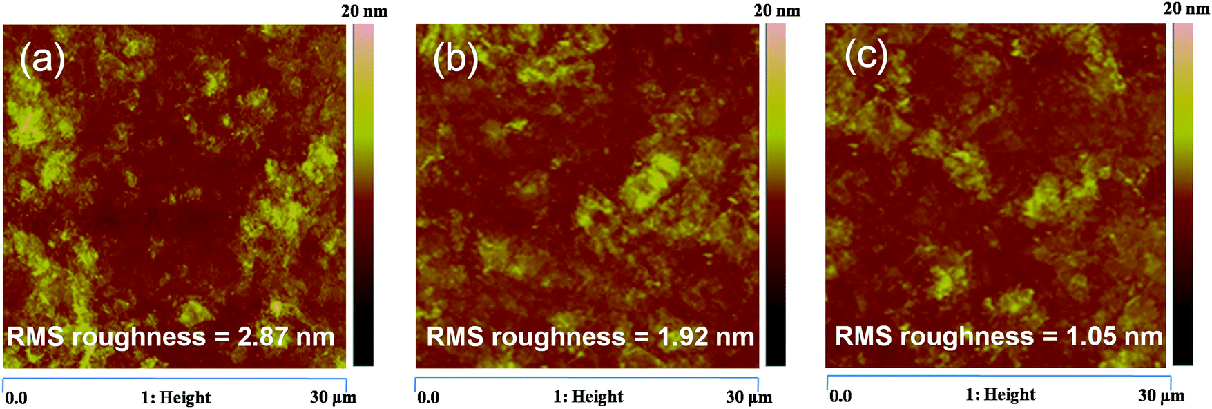 | ||
| Fig. 8 (a–c) AFM images of the P3HT:PCBM binary blend, PTB7-Th:PCBM binary blend, and P3HT:PTB7-Th:PCBM ternary blend, respectively. | ||
Furthermore, to understand the effect of the carrier mobilities on exciton dissociation and carrier collection and its correlation with the charge transport properties of the ternary blend, we calculated the exciton dissociation efficiency Pdiss(E,T), charge collection efficiency Pcoll(E,T) and exciton generation rate (Gmax) by analyzing the photocurrent density (Jph) as a function of effective voltage (Veff) for the P3HT:PTB7-Th:PCBM based TPSCs and compared with that of the P3HT:PCBM and PTB7-Th:PCBM binary blend devices, respectively. Fig. 9(a) depicts the dependence of the measured Jph on Veff in the three devices. Here, Jph = JL − JD, where JL and JD are the current densities under illumination and in the dark, respectively. Veff = V0 − Vapp, where V0 is the voltage at which Jph = 0 and Vapp is the applied voltage.
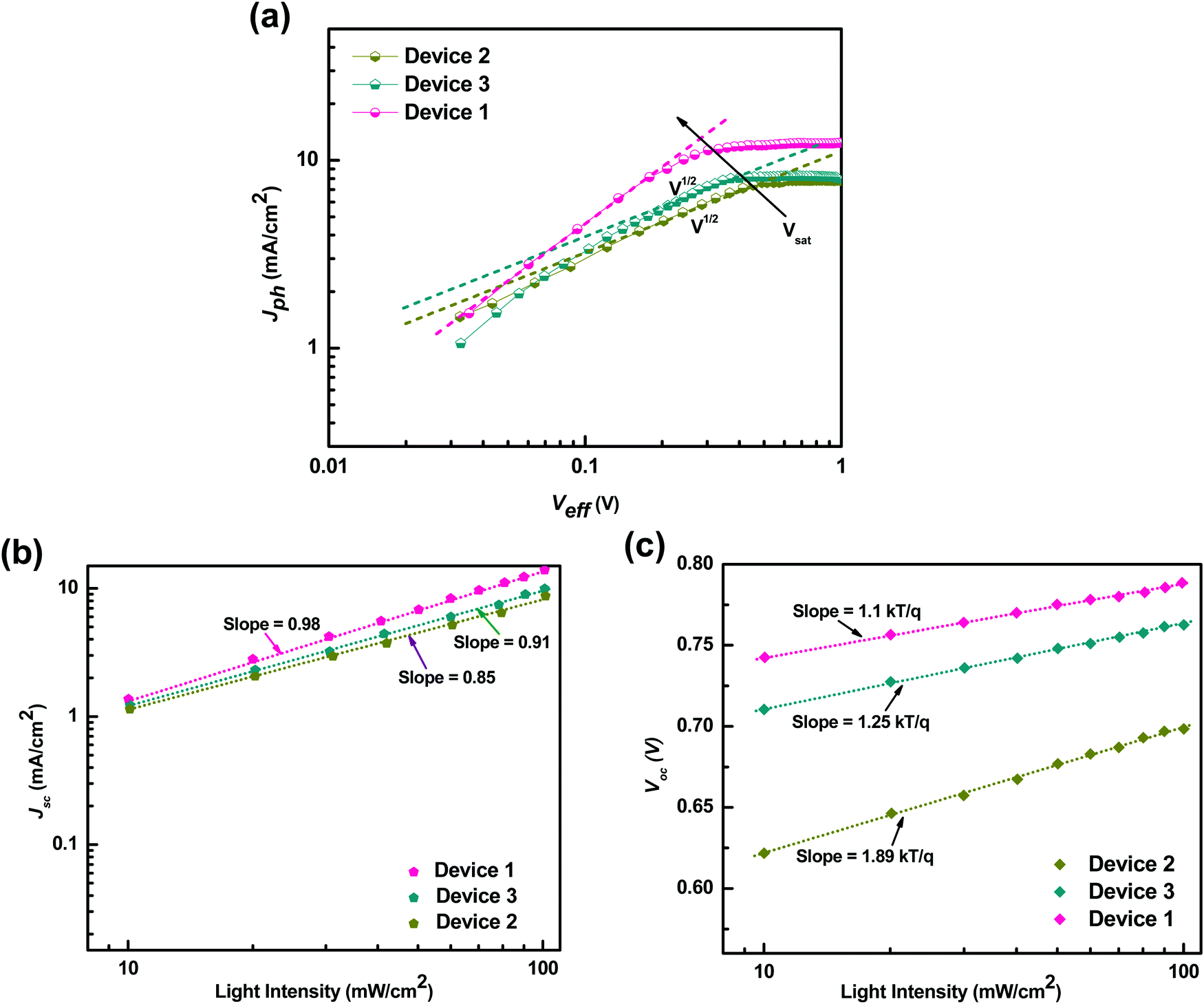 | ||
| Fig. 9 (a) Photocurrent density (Jph) as a function of effective voltage for the devices with binary and ternary blends. (b) Jphvs. light intensity. (c) Vocvs. light intensity. | ||
Apparently, Jph increases linearly at very low voltages in Device 2 and Device 3, but Jph is proportional to V1/2 at intermediate voltages and finally tends to saturate at high Veff voltages. This means that at high voltages, the internal field is sufficiently large to sweep out all the dissociated carriers from the device. At comparatively intermediate voltages, a large V1/2 regime is observed in Device 2 compared to Device 3, implying that the space charge limited (SCL) photocurrent prevails in the P3HT:PCBM blend whereas recombination (μτ) limited photocurrent governs in the case of PTB7-Th:PCBM blends.51 The origin of SCL photocurrent/recombination (μτ) limited photocurrent is determined by the imbalance of electron and hole mobilities in the blend, which in turn is decided by the μe/μh ratio in these blends.51,52 As μe/μh = 125 in P3HT:PCBM, which is very large, SCL photocurrent is observed, and μe/μh = 40, which is relatively low and is accountable for the recombination (μτ) limited photocurrent in PTB7-Th:PCBM blends. However, in the P3HT:PTB7-Th:PCBM ternary blend based Device 1, the V1/2 regime disappears completely, i.e., the curve is linear at low and intermediate regimes. This is primarily due to a very low ratio of μe/μh = 1.81 and signifies that photocurrent is not limited by recombination or space charge primarily due to balanced electron and hole transport. Another effect observed is that Vsat shifts to a lower voltage of 0.3 V in Device 1, compared to Vsat = 0.46 V (Device 2) and Vsat = 0.34 V (Device 3). This could be understood with regard to the dielectric constant. The P3HT:PTB7-Th (0.3:0.7) blend includes a higher dielectric constant polymer (εr = 3.5) blended with a low dielectric constant polymer (εr = 3), hence leading to εr = 3.35 for the ternary blend. As we know that the exciton binding energies are inversely proportional to the dielectric constant of the materials, therefore, we can say that the excitonic energies decrease in PTB7-Th and P3HT:PTB7-Th (0.3:0.7) blends compared to P3HT. Hence, this causes all the photo-generated excitons to dissociate into free charge carriers easily and effectively at a relatively lower field. On the other hand, Jsat, which is limited by the number of photons absorbed by the active layer, is given by Jsat = qLGmax, where L is film thickness, and Gmax is the maximum generation rate. Jsat increases from 7.7 mA cm−2 in P3HT:PCBM Device 2 to 8.16 mA cm−2 in PTB7-Th:PCBM Device 3, which increases further to 12.1 mA cm−2 in P3HT:PTB7-Th (0.3:0.7) ternary blend Device 1. Gmax calculated from Jsat is 2.62 × 1027 m−3 s−1 for Device 1, which is much higher than the values 1.67 × 1027 m−3 s−1 for Device 2 and 1.77 × 1027 m−3 s−1 for Device 3. The enhancement in Gmax is attributed to the enhanced light absorption band of the ternary blend obtained in the UV-Vis absorption spectra whereas both the binary blends exhibit a narrow absorption band. The exciton dissociation efficiency P(E,T), which depends on electric field and temperature, is calculated as45,47Pdiss(E,T) = J(SC)ph/Jsat, and the charge collection efficiency is Pcoll(E,T) = J(MPP)ph/Jsat, where J(SC)ph and J(MPP)ph are the Jph values under a short circuit condition and at the maximum power point, respectively. As calculated, Pdiss = 92.6% and Pcoll = 84.3% for P3HT:PTB7-Th:PCBM (0.3:0.7:1) ternary blend Device 1, which is much higher compared to that of the binary devices, i.e., Pdiss = 80.7% and Pcoll = 76.3% for P3HT:PCBM and Pdiss = 81.5% and Pcoll = 78.9% for PTB7-Th:PCBM. These results confirm that the exciton dissociation, carrier generation, charge transport, and charge collection processes are indeed more efficient in the P3HT:PTB7-Th:PCBM ternary blend with the (0.3:0.7:1) composition. This is in coherence with the high Jsc and FF obtained in these devices.
To build more understanding for the increase of Jsc and FF in the ternary blends, we probed the recombination kinetics, by studying the Jsc and Voc under illumination with different intensities, shown in Fig. 9(b and c). It is well known that Jsc and light intensity (IL) obey the power-law, i.e., Jsc ∝ IaL, where exponent a describes the bimolecular loss.45,47 If a is close to unity, then bimolecular losses are very weak. A deviation from a ≈ 1 suggests strong bimolecular losses. Fig. 9(b) shows Jscvs. IL on a log–log scale for Device 1, Device 2, and Device 3. The values are fitted with the power-law as described above. a = 0.85 and a = 0.91 were obtained for binary blend based Devices 2 and 3, suggesting that photo-carriers are not swept away from the active layer blend easily under short circuit conditions. They slow down due to strong bimolecular recombination in the P3HT:PCBM blend, which relatively weakens in PTB7-Th:PCBM blends, owing to the high density of traps present in the P3HT:PCBM blend and a lower trap density in PTB7-Th:PCBM matrices (as discussed earlier). Such bimolecular recombination limits the exciton dissociation after charge transfer (interface CT entities) and greatly deteriorates the charge separation and transport, and hence, low Jsc and FF are observed in these binary blend devices. On the other hand, a increases to 0.98, which is close to unity, implying that almost no bimolecular recombination or very weak recombination occurs in ternary blends, confirming further the trap-free charge transport owing to large charge carrier mobilities, high Rsh (Table 2), and, hence, the enhanced Jsc and FF obtained in the TPSCs.
Furthermore, the dependence of Voc on IL describes the nature of recombination in these binary and ternary blends. The Voc follows the relation Voc = nkBT/q[ln(IL)], where q is the elementary charge, kB is the Boltzmann constant, T is the absolute temperature, and n is the ideality factor.45 Here, the slope of Vocvs. ln(IL) is equal to kT/q, which means bimolecular recombination losses, and 2kT/q signifies trap assisted-Shockley Read–Hall (SRH) recombination losses. The plot of Vocvs. IL is shown in Fig. 9(c). The slope = 1.89kT/q for Device 2 suggests that only trap assisted-SRH recombination exists in the P3HT:PCBM blend, whereas in the PTB7-Th:PCBM blend, slope = 1.25kT/q, which signifies that both bimolecular and trap assisted-SRH recombinations coexist yet the effect is weak. However, in the P3HT:PTB7-Th:PCBM ternary blend, a slope close to 1.1kT/q proves very weak recombination losses exclusively due to bimolecular recombination accounting for the fast charge transport observed in these ternary blends.
Effect of the PEDOT:PSS–GO HTL on the photovoltaic performance of TPSCs
To further inspect the effect of GO on PEDOT:PSS HTLs on the charge dissociation and recombination processes at the HTL/active layer interface, we compared the J–V characteristics of the P3HT:PTB7-Th:PCBM (0.3:0.7:1) ternary blend with the PEDOT:PSS–GO HTL (Device 1) and with the only-PEDOT:PSS HTL (Device 4) under Air Mass 1.5 Solar illumination (Pin = 100 mW cm−2), as shown in Fig. S6 (see the ESI†). The device parameters obtained (mentioned in Table S3 in the ESI†) reveal that there is a significant improvement in PCE from 3.2% in TPSC Device 4 (with only-PEDOT:PSS HTL) to 7.1% in TPSC Device 1 (with only-PEDOT:PSS–GO HTL), as there is a low Jsc (10.7 mA cm−2), Voc (0.69) and poor FF (0.43) in Device 4. This improvement in device performance upon the addition of GO into the PEDOT:PSS HTL is due to (i) lowering of the interface potential barrier at the HTL/active layer interface due to an increase in work function, (ii) low recombination at surface traps owing to efficient electron blocking properties, and (iii) a higher σ of the PEDOT:PSS–GO films, as already discussed. Hence, we conclude that the incorporation of GO nanosheets into PEDOT:PSS improves the carrier extraction and supports fast transport of carriers at the anode, making PEDOT:PSS–GO composites potential HTL for TPSCs.
Stability of TPSCs
The fabricated devices were tested for degradation, and the studies were extended to examine the stability of the fabricated TPSC devices, as described elsewhere.29 For stability studies, the measurements were taken every 50–100 h of storage. The stability characteristics of TPSC Device 1 were compared with binary blend Device 2 (P3HT:PCBM) and Device 3 (PTB7-Th:PCBM), and also with TPSC Device 4 (with only-PEDOT:PSS HTL). Fig. 10(a–d) shows the stability characteristics of all the Devices representing the normalized PCE, normalized Jsc, normalized Voc, and normalized FF. On comparing the data of Device 1 with those of Device 2 and Device 3, we observed that the devices with P3HT:PTB7-Th:PCBM (0.3:0.7:1) ternary blends showed better stability compared to (P3HT:PCBM) and (PTB7-Th:PCBM) binary blend devices, where PCE is retained for 500 h with only 10% reduction from its initial value. The only-PEDOT:PSS based TPSC Device 4 is more unstable with a 33% loss of PCE, compared to PEDOT:PSS–GO HTL based TPSC Device 1. This instability is due to the hygroscopic nature of PEDOT:PSS, which absorbs moisture and water molecules may diffuse into the active layer, leading to the degradation of only-PEDOT:PSS based TPSCs. On the other hand, when PEDOT:PSS–GO shows more stability owing to the good thermal and photo-stability of GO nanosheets, degradation is reduced in TPSCs with PEDOT:PSS–GO HTLs. Hence, [P3HT:PTB7-Th:PC71BM] (0.3:0.7:1) ternary blend based TPSCs using PEDOT:PSS–GO (1:1) display good performance and stability.
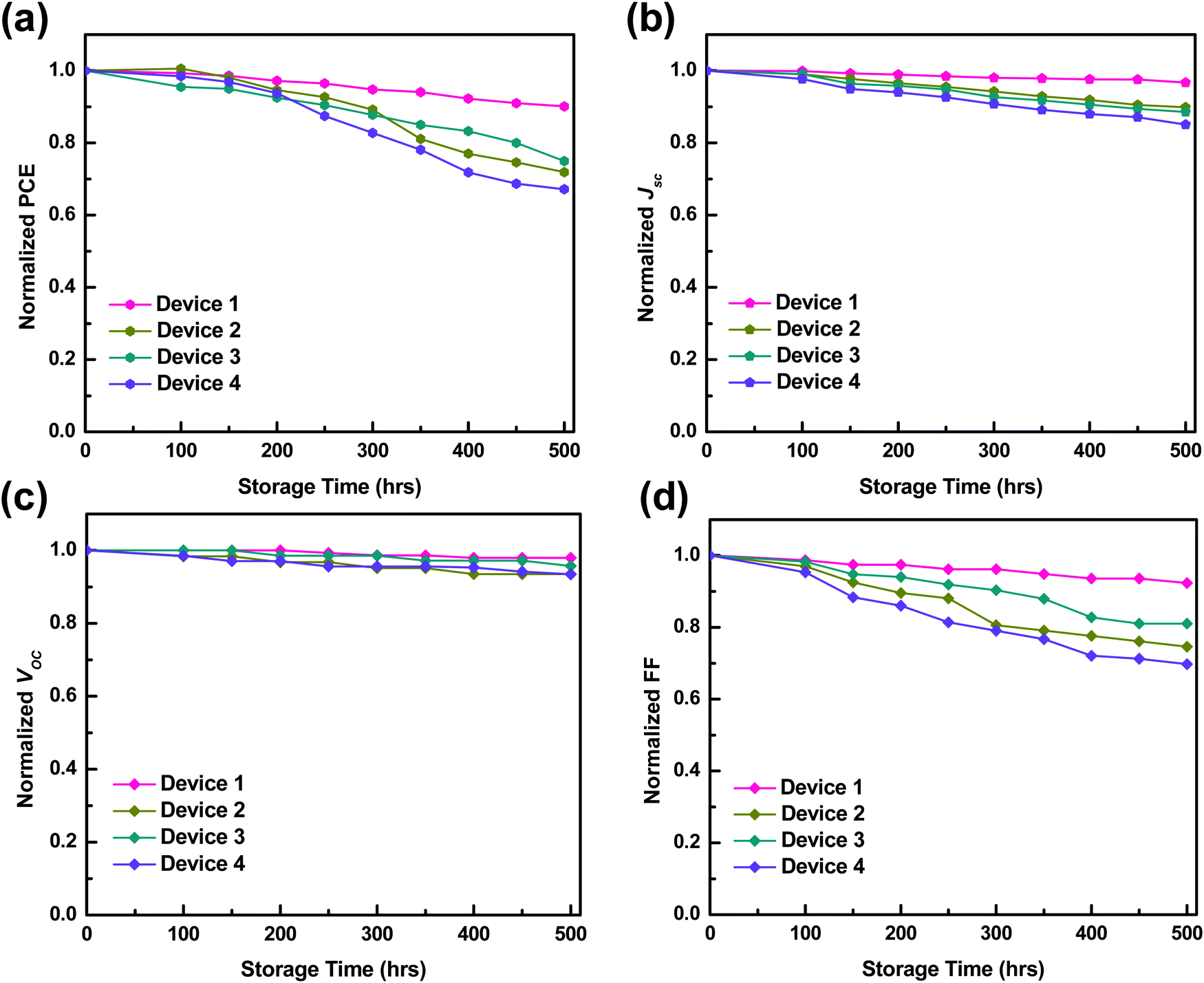 | ||
| Fig. 10 Stability characteristics of Device 1, Device 2, Device 3, and Device 4. (a) Normalized PCE. (b) Normalized Jsc. (c) Normalized Voc. (d) Normalized FF. | ||
Experimental
Materials
GO was prepared by using a modified Hummers method.36,37 Briefly, 1.5 g of graphite flakes (Alfa Aesar with 99.99% purity) was exfoliated in a microwave for 10 s. The exfoliated graphite flakes obtained and 250 ml of H2SO4 were mixed in a 1000 ml volumetric flask and kept in an ice bath under continuous stirring. Then, the sample mixture was stirred at 300 rpm for 2 h at room temperature and subsequently 10.5 g of potassium permanganate (KMnO4) was slowly added to the suspension. The addition rate was controlled vigilantly to maintain the reaction temperature at 98 °C. After this, 1.5 litres of water was added. This decreases the temperature of the sample mixture below 98 °C, hence, immediately the temperature was raised again to maintain at 98 °C. Finally, 30 ml of H2O2 was added to the stirring mixture and the reaction was terminated. The precipitate of the resultant mixture was filtered to obtain GO powder. For purification, the mixture was washed with 90 ml of hydrochloric acid (HCl) and 900 ml of deionized water (DI) water and stirred at 400 rpm for 30 min. The solution was centrifuged at 4000 rpm for 15 min to remove un-exfoliated GO. Later, the filtered mixture was washed with 1 litre of distilled water and stirred at 400 rpm continuously for 1 h. Again, it was centrifuged at 4000 rpm for 30 min and the un-exfoliated GO was removed. Finally, the mixture was filtered and then dried in an oven to obtain GO powder.Device fabrication
For TPSC device fabrication, GO nanosheet powder was exfoliated in DI water (100 mg ml−1) and sonicated for an hour. PEDOT:PSS, regioregular P3HT, PTB7-Th, and PCBM were procured from Sigma Aldrich USA, and were used without any further purification.Solar cell devices were fabricated in the following device configuration, Device 1: ITO/PEDOT:PSS–GO (1:1) (∼40 nm)/P3HT:PTB7-Th:PCBM (0.3:0.7:1) (∼180 nm)/LiF/Al, Device 2: ITO/PEDOT:PSS–GO (1:1) (∼40 nm)/P3HT:PCBM (1:1) (∼180 nm)/LiF/Al, Device 3: ITO/PEDOT:PSS–GO (1:1) (∼40 nm)/PTB7-Th:PCBM (1:1) (∼180 nm)/LiF/Al, and Device 4: ITO/PEDOT:PSS (∼40 nm)/P3HT:PTB7-Th:PCBM (0.3:0.7:1) (∼180 nm)/LiF/Al. For device fabrication, indium tin oxide (ITO) coated glass (sheet resistance ∼15 Ω □−1) substrates were cleaned using a soap solution, DI water, acetone, and isopropanol, by sonication (10 min each step). The cleaned and dried ITO substrates were then treated with ultra-violet ozone (UVO) for 15 min. For the HTL, GO nanosheets were dispersed in the PEDOT:PSS solution in a 1:1 ratio by weight and sonicated for 30 min. A thin film of PEDOT:PSS–GO (HTL) was spin-coated onto precleaned and ITO substrates at 2000 rpm for 50 s and cured at 120 °C for 30 min in a vacuum. For Device 4, a pure PEDOT:PSS HTL solution was spin-coated by following the same procedure as above. This results in a thin film of thickness ∼40 nm. Next, for the active layer, first, a solution of P3HT and PCBM has been prepared in chlorobenzene solvent in a 1:1 weight ratio (20 mg ml−1) and, similarly, a solution of PTB7-Th and PCBM has been prepared in 1,8-diiodoctane (97:3 vol%) solvent in a 1:1 weight ratio with a concentration of 20 mg ml−1. For the ternary blend, a solution of P3HT, PTB7-Th and PCBM has been prepared in a 0.3:0.7:1 weight ratio in a mixed solvent of chlorobenzene and 1,8-diiodoctane (1:3 vol%) with a concentration of 20 mg ml−1. All the polymer blend solutions were filtered with a 0.2 μm filter. For all the devices, the active layer was spin-coated on HTL coated ITO substrates using the respective solutions at 2000 rpm for 1 min in a glove box, and cured at 120 °C for 10 min. On top of the active layer films, LiF/Al electrodes of ∼100 nm were deposited by thermal evaporation at a vacuum of 5 × 10⁻⁶ Torr. The active area was ∼0.1 cm2 for all the devices.
Characterization and measurement
The transmittance and absorption spectra of GO, PEDOT:PSS and PEDOT:PSS–GO HTL thin films were recorded using a V-670 UV-visible spectrometer (Jasco) at wavelengths in the region of 200–850 nm. XRD was performed using an X-ray diffractometer (PANalytical X'PERT-PRO with CuKα (λ = 0.1542 nm) radiation). Morphological studies of GO, PEDOT:PSS–GO, and active layer films were carried out via FESEM (Hitachi High-Technologies S-4800) and AFM (Veeco DI-3100). A confocal Raman spectrometer (WITec alpha300R) was used to record Raman spectra with a laser excitation of wavelength 532 nm. UPS measurements were performed using an electron spectrometer, Scienta R4000, using a helium (I) (21.2 eV) source. The PL and TRPL (via time-correlated single-photon count) spectra of the films were recorded using a Horiba quantamaster 800 fluorometer in the wavelength region of 450–850 nm. The solar cell J–V characteristics were measured using a solar simulator (Newport-Oriel) with an Air Mass 1.5G filter at a light intensity of 100 mW cm−2 interfaced with a Keithley 2400 source measurement unit (SMU). The devices were illuminated from the transparent ITO electrode side using the solar simulator. The light intensity was determined by calibration with a standard silicon photodiode (Newport). The external quantum efficiency (EQE) spectra were recorded using a Newport-Oriel IQE-200B over the wavelength range of 300–800 nm. All measurements were performed at room temperature. The J–V characteristics of hole-only devices in the configuration ITO/PEDOT:PSS/polymer/Au were measured using a Keithley 2400 SMU at room temperature. For the P3HT based hole-only device, i.e., ITO/PEDOT:PSS/P3HT/Au, the J–V characteristics were measured at different temperatures, 288–95 K.Conclusion
We fabricated [P3HT:PTB7-Th:PC71BM] (0.3:0.7:1) ternary blend based TPSCs using PEDOT:PSS–GO (1:1) composite HTLs. In order to illustrate the advantages of ternary blends, the J–V characteristics of the TPSC device was compared with the respective binary counterparts, i.e., devices with P3HT:PCBM and PTB7-Th:PCBM binary blends. Also, to understand the effect of GO in the PEDOT:PSS HTL, we performed a comparison with the TPSCs fabricated using only-PEDOT:PSS HTLs. It has been found that these TPSCs showed significant improvements in performance and stability with PCE ∼ 7.1% and this was retained for 500 hours with only a 10% loss from its initial value. The enhancement in photovoltaic performance exhibited by P3HT:PTB7-Th:PC71BM TPSCs was attributed to the synergetic effect of the P3HT:PC71BM and PTB7-Th:PC71BM binary counterparts is owing to (i) strong and complementary absorption by P3HT and PTB7-Th molecules leading to a broad spectral response with photon-to-electron conversion approaching 67–75% in the extended wavelength range of 350–780 nm, as confirmed by EQE spectra; (ii) PL quenching and photo-carrier dynamics studies demonstrated that photo-exciton lifetime decreases drastically from τ1 = 129 ps (in P3HT) to τ1 = 17 ps (in P3HT:PTB7-Th:PCBM), which is a consequence of both FRET and CT owing to the cascade energy level alignment, resulting in effective exciton dissociation in the ternary blend; (iii) the improved quality of P3HT:PTB7-Th:PC71BM active layer thin films as compared to P3HT:PC71BM and PTB7-Th:PC71BM binary blend films resulting in improved hole mobilities (μe/μh ratio ∼1.81) resulting in balanced charge transport governed by the trap-free SCLC with very weak bimolecular recombination losses; (iv) the four probe conductivity and ultraviolet photo absorption measurements revealed that the addition of GO nanosheets in PEDOT:PSS imparts a high σ, and increases Φ, making the HOMO level match well with the HOMO of the polymer donors of the active layers, lowering the potential barrier, facilitating charge extraction at the HTL/active layer interface; (v) PEDOT:PSS–GO possesses better electron blocking capability, promoting the carrier collection at the anode without interface-state recombination at the HTL/active layer interface. The advantageous properties of (P3HT:PTB7-Th:PC71BM) ternary blend PEDOT:PSS–GO composite HTLs collectively boost the performance of the TPSCs. All these results make these devices a potential candidate to take TPSCs towards their ultimate goal of envisaged commercialization.
Conflicts of interest
The author(s) declare no conflict of interest.Acknowledgements
The authors gratefully acknowledge the financial support received from the research project sponsored by the Department of Science & Technology, Science and Engineering Research Board, Government of India, under the Empowerment and Equity Opportunities for Excellence in Science program (project no. EEQ/2016/000723); and also from the project sponsored by the Department of Science & Technology, Technology Mission Division, Government of India, under the Solar Energy Research Initiative program (project no. DST/TMD/SERI/S56(C)).References
- M. Scharber and N. Sariciftci, Prog. Polym. Sci., 2013, 38, 1929 CrossRef CAS.
- S. Foster, F. Deledalle, A. Mitani, T. Kimura, K.-B. Kim, T. Okachi, T. Kirchartz, J. Oguma, K. Miyake, J. R. Durrant, S. Doi and J. Nelson, Adv. Energy Mater., 2014, 4, 1400311 CrossRef.
- Y. Huang, E. Kramer, A. Heeger and G. Bazan, Chem. Rev., 2014, 114, 7006 CrossRef CAS.
- G. Wang, F. Melkonyan, A. Facchetti and T. Marks, Angew. Chem., Int. Ed., 2019, 58, 4129 CrossRef CAS.
- C. Lee, S. Lee, G. Kim, W. Lee and B. Kim, Chem. Rev., 2019, 119, 8028 CrossRef CAS.
- X. Xu, K. Feng, Z. Bi, W. Ma, G. Zhang and Q. Peng, Adv. Mater., 2019, 31, 1901872 CrossRef.
- R. Gurney, D. Lidzey and T. Wang, Rep. Prog. Phys., 2019, 82, 036601 CrossRef CAS.
- A. Karki, J. Vollbrecht, A. Dixon, N. Schopp, M. Schrock, G. Reddy and T. Nguyen, Adv. Mater., 2019, 31, 1903868 CrossRef CAS.
- Y. Lin, Y. Firdaus, M. I. Nugraha, F. Liu, S. Karuthedath, A.-H. Emwas, W. Zhang, A. Seitkhan, M. Neophytou, H. Faber, E. Yengel, I. McCulloch, L. Tsetseris, F. Laquai and T. D. Anthopoulos, Adv. Sci., 2020, 7, 1903419 CrossRef CAS.
- H. Yin, C. Yan, H. Hu, J. Ho, X. Zhan, G. Li and S. So, Mater. Sci. Eng., R, 2020, 140, 100542 CrossRef.
- S. H. Park, A. Roy, S. Beaupré, S. Cho, N. Coates, J. S. Moon, D. Moses, M. Leclerc, K. Lee and A. J. Heeger, Nat. Photonics, 2009, 3, 297 CrossRef CAS.
- D. Huang, Y. Li, Z. Xu, S. Zhao, L. Zhao and J. Zhao, Phys. Chem. Chem. Phys., 2015, 17, 8053 RSC.
- L. Fernandes, H. Gaspar, J. P. C. Tomé, F. Figueira and G. Bernardo, Polym. Bull., 2017, 75, 515 CrossRef.
- H.-Y. Chen, J. Hou, S. Zhang, Y. Liang, G. Yang, Y. Yang, L. Yu, Y. Wu and G. Li, Nat. Photonics, 2009, 3, 649 CrossRef CAS.
- T. Ameri, P. Khoram, J. Min and C. J. Brabec, Adv. Mater., 2013, 25, 4245 CrossRef CAS.
- L. Yang, L. Yan and W. You, J. Phys. Chem. Lett., 2013, 4, 1802 CrossRef CAS.
- Y. Yang, W. Chen, L. Dou, W.-H. Chang, H.-S. Duan, B. Bob, G. Li and Y. Yang, Nat. Photonics, 2015, 9, 190 CrossRef CAS.
- Z. S. Wang, X. Ren, X. Xu, Q. Peng, W. E. I. Sha and W. C. H. Choy, Nano Energy, 2018, 51, 206 CrossRef CAS.
- B. Fan, W. Zhong, X.-F. Jiang, Q. Yin, L. Ying, F. Huang and Y. Cao, Adv. Energy Mater., 2016, 7, 1602127 CrossRef.
- W. Chen, H. Jiang, G. Huang, J. Zhang, M. Cai, X. Wan and R. Yang, Sol. RRL, 2018, 2, 1800101 CrossRef.
- H. Yin, S. H. Cheung, J. H. L. Ngai, C. H. Y. Ho, K. L. Chiu, X. Hao, H. W. Li, Y. Cheng, S. W. Tsang and S. K. So, Adv. Electron. Mater., 2017, 3, 1700007 CrossRef.
- J. Mai, T.-K. Lau, T. Xiao, C.-J. Su, U.-s. Jeng, N. Zhao, X. Xiao and X. Lu, RSC Adv., 2015, 5, 88500 RSC.
- K. Nakano, K. Suzuki, Y. Chen and K. Tajima, Sci. Rep., 2016, 6, 29529 CrossRef CAS.
- P. P. Khlyabich, A. E. Rudenko, B. C. Thompson and Y.-L. Loo, Adv. Funct. Mater., 2015, 25, 5557 CrossRef CAS.
- J. Huang, H. Wang, K. Yan, X. Zhang, H. Chen, C.-Z. Li and J. Yu, Adv. Mater., 2017, 29, 1606729 CrossRef.
- L. Lu, M. A. Kelly, W. You and L. Yu, Nat. Photonics, 2015, 9, 491 CrossRef CAS.
- T. Goh, J.-S. Huang, B. Bartolome, M. Y. Sfeir, M. Vaisman, M. L. Lee and A. D. Taylor, J. Mater. Chem. A, 2015, 3, 18611 RSC.
- G. Adam, B. Munkhbat, P. Denk, C. Ulbricht, C. Hrelescu and M. C. Scharber, Front. Mater., 2016, 3, 39 Search PubMed.
- M. Hilal and J. I. Han, Sol. Energy, 2018, 167, 24 CrossRef CAS.
- S.-S. Li, K.-H. Tu, C.-C. Lin, C.-W. Chen and M. Chhowalla, ACS Nano, 2010, 4, 3169 CrossRef CAS.
- J. Liu, Y. Xue, Y. Gao, D. Yu, M. Durstock and L. Dai, Adv. Mater., 2012, 24, 2228 CrossRef CAS.
- J. C. Yu, J. A. Hong, E. D. Jung, D. B. Kim, S.-M. Baek, S. Lee, S. Cho, S. S. Park, K. J. Choi and M. H. Song, Sci. Rep., 2018, 8, 1070 CrossRef.
- X. Wu, J. Liu, D. Wu, Y. Zhao, X. Shi, J. Wang, S. Huang and G. He, J. Mater. Chem. C, 2014, 2, 4044 RSC.
- A. Iwan, F. Caballero-Briones, M. Filapek, B. Boharewicz, I. Tazbir, A. Hreniak and J. Guerrero-Contreras, Sol. Energy, 2017, 146, 230 CrossRef CAS.
- Y.-F. Liu, J. Feng, Y.-F. Zhang, H.-F. Cui, D. Yin, Y.-G. Bi, J.-F. Song, Q.-D. Chen and H.-B. Sun, Org. Electron., 2015, 26, 81 CrossRef CAS.
- J. T. Han, B. J. Kim, B. G. Kim, J. S. Kim, B. H. Jeong, S. Y. Jeong, H. J. Jeong, J. H. Cho and G.-W. Lee, ACS Nano, 2011, 5, 8884 CrossRef CAS.
- J. C. Yu, J. I. Jang, B. R. Lee, G.-W. Lee, J. T. Han and M. H. Song, ACS Appl. Mater. Interfaces, 2014, 6, 2067 CrossRef CAS.
- T. A. Amollo, G. T. Mola and V. O. Nyamori, Sol. Energy, 2018, 171, 83 CrossRef CAS.
- N. Díez, A. Śliwak, S. Gryglewicz, B. Grzyb and G. Gryglewicz, RSC Adv., 2015, 5, 81831 RSC.
- R. Yu, H. Yao and J. Hou, Adv. Energy Mater., 2018, 1702814, 1–9 Search PubMed.
- J.-S. Yeo, R. Kang, S. Lee, Y.-J. Jeon, N. Myoung, C.-L. Lee, D.-Y. Kim, J.-M. Yun, Y.-H. Seo, S.-S. Kim and S.-I. Na, Nano Energy, 2015, 12, 96 CrossRef CAS.
- F. Wang, X.-Y. Yang, M.-S. Niu, L. Feng and X.-T. Hao, Org. Electron., 2019, 67, 146 CrossRef CAS.
- I.-W. Hwang, J. Kong, H. K. Yoo and K. Lee, J. Phys. Chem. C, 2015, 119, 12896 CrossRef CAS.
- K. Kumari, S. Chand, P. Kumar, S. N. Sharma, V. D. Vankar and V. Kumar, Appl. Phys. Lett., 2008, 92, 263504 CrossRef.
- Y. Liu, B. He, J. Duan, Y. Zhao, Y. Ding, M. Tang, H. Chen and Q. Tang, J. Mater. Chem. A, 2019, 7, 12635 RSC.
- S. J. Sung, J. H. Kim, S. H. Gihm, J. Park, Y. S. Cho, S. J. Yang and C. R. Park, ACS Appl. Energy Mater., 2019, 2(12), 8826 CrossRef CAS.
- H. Wang, J. Huang, S. Xing and J. Yu, Org. Electron., 2016, 28, 11 CrossRef CAS.
- D. Liu, P. Fan, D. Zhang, X. Zhang and J. Yu, Sol. Energy, 2019, 189, 186 CrossRef CAS.
- B. Wang, Y. Fu, C. Yan, R. Zhang, Q. Yang, Y. Han and Z. Xie, Front. Chem., 2018, 6, 198 CrossRef.
- H. T. Nicolai, M. Kuik, G. A. H. Wetzelaer, B. de Boer, C. Campbell, C. Risko, J. L. Brédas and P. W. M. Blom, Nat. Mater., 2012, 11, 882 CrossRef CAS.
- V. D. Mihailetchi, J. Wildeman and P. W. M. Blom, Phys. Rev. Lett., 2005, 94, 126602 CrossRef CAS.
- M. Lenes, M. Morana, C. J. Brabec and P. W. M. Blom, Adv. Funct. Mater., 2009, 19, 1106 CrossRef CAS.
Footnote |
| † Electronic supplementary information (ESI) available. See DOI: 10.1039/d0ma00532k |
| This journal is © The Royal Society of Chemistry 2020 |