
 Open Access Article
 This Open Access Article is licensed under a Creative Commons Attribution-Non Commercial 3.0 Unported Licence
Effect of access resistance on the experimentally measured temperature–carrier mobility dependence in highly-crystalline DNTT-based transistors†
Qijing
Wang
,
Sai
Jiang
,
Yi
Shi
* and
Yun
Li
 *
*
National Laboratory of Solid-State Microstructures, School of Electronic Science and Engineering, Collaborative Innovation Center of Advanced Microstructures, Nanjing University, Nanjing 210093, P. R. China. E-mail: yli@nju.edu.cn; yshi@nju.edu.cn
First published on 23rd July 2020
Abstract
Carrier mobility extraction is easily influenced by contact resistance, especially in transistors with a high carrier mobility and a short channel length, which would obscure the investigation into charge transport in organic field-effect transistors (OFETs). Here, we perfunctorily observe a positive carrier mobility–temperature relationship (∂μ/∂T > 0) and a temperature-independent carrier mobility (∂μ/∂T = 0) in OFETs based on less- and highly-crystalline DNTT bulk films, respectively, while their room-temperature carrier mobilities are almost identical. The difference in the temperature–carrier mobility dependence is attributed to the influence of access resistance while the active channels at the semiconductor/dielectric interface were deposited by the same process of different evaporation rates, which leads to different contact resistances tuned by the DNTT molecular packing in the c-axis. Therefore, it will be beneficial for investigating the charge transport of organic semiconductors by eliminating the influence of access resistance in staggered OFETs.
Introduction
Organic field-effect transistors (OFETs) have gained great attention and shown fundamental progress in the physical mechanism of charge transport over recent decades.1–4 The charge transport in most OFETs is likely to be in a hopping mode in which charge carriers are in localized states, while only a few OFETs with high carrier mobilities (> 1 cm2 V−1 s−1) and nearly trap-free semiconductor/dielectric interfaces can exhibit a bandlike charge transport with ∂μ/∂T < 0, where μ is the carrier mobility and T is the temperature.5–7 In principle, long-range charge delocalization, requiring strong π–π orbital overlapping, in active channels is one key factor to realize bandlike charge transport in organic semiconductors.8,9 Additionally, in molecular organic semiconductors, transfer integrals among molecules in the c-axis are much lower compared with those in the ab-plane in the active channels. However, the energy barriers between the contact and the channel are unavoidable in OFET structures. According to Matthiessen's rule,10–12 the calculated carrier mobility can be expressed as μFET−1 = μch−1 + μac−1, where μch and μac are the carrier mobilities in the channel and the access region, respectively. Therefore, μac plays a significant role in the overall device performance. In addition, the μFET value of OFETs with high contact resistance may present an inaccurate temperature-dependent charge transport.11,12 The observed weakly temperature-dependent charge transport under some circumstances, especially in high-mobility organic semiconductors, should be further checked by excluding the effect of μac.13In our previous work, we found that a high-quality semiconductor/dielectric interface with an interfacial layer could effectively suppress the dipole localization and polarization and facilitate the formation of smooth charge transport with a low activation energy.14,15 Here, we further observed temperature-independent charge transport with a carrier mobility above 2.0 cm2 V−1 s−1 in OFETs based on dinaphtho[2,3-b:2′,3′-f]thieno[3,2-b] thiophene (DNTT) films deposited by slow thermal evaporation. The μ–T relationship could be adjusted by changing the evaporation rate of the access region (the upper layers in DNTT films) which could influence the film crystallinity and molecular packing, especially in the c-axis. By excluding the effect of μac and access resistance, the initially observed ∂μ/∂T > 0 in DNTT OFETs turned to be nearly ∂μ/∂T = 0 (temperature-independent). Taking μac into consideration can facilitate the attainment of an accurate temperature–carrier mobility relationship in OFETs, which is essential for the understanding of device physics in OFETs.
Results and discussion
The DNTT films were deposited via a thermal evaporation process which will be introduced in the Experimental section.15,16 In this work, we first prepared the DNTT films with various thicknesses of 4 nm, 10 nm, 20 nm, and 50 nm through slow thermal evaporation. The surface morphology of all DNTT films was characterized by the atomic force microscopy (AFM) (Fig. 1a). The DNTT samples with thicknesses of 4 and 10 nm show an obvious layered structure and exhibit uniform surfaces. When the film thickness increases to 20 nm, a typical step-and-terrace structure is observed while some nanoclusters start to exist randomly. This is because the DNTT molecules are easily affected by the increasing energetic disorders and temperature fluctuations along with the increasing distance between the DNTT molecules and the SiO2 dielectric.17,18 Furthermore, the 50 nm-thick samples possess many domains and cracks, resulting in large nonuniformity and discontinuity. To further evaluate the crystalline properties of all DNTT films, the X-ray diffraction (XRD) characterizations were carried out (Fig. 1b). Typical peaks at 2θ = 5.12°, 5.31°, and 5.37°, corresponding to the (001) lattice plane, in 10 nm, 20 nm, and 50 nm-thick DNTT samples are observed and this peak becomes sharper and more intensive with the increasing film thickness. The positive shift of the (001) peak indicates the weakening of the van der Waals interaction between DNTT molecules and the substrate while the molecular packing approaches the intrinsic one in single crystals (2θ = 5.44°).13 Besides, the (003) peak can be seen in 20 nm and 50 nm-thick samples while the (002) peak is only observed in the 50 nm-thick DNTT film. Surprisingly, obvious reflection fringes are observed in these DNTT samples, especially in the 20 nm and 50 nm-thick films, suggesting that the slow-evaporated DNTT films possess extremely high crystallinity with ordered and layered molecular packing in the c-axis direction in a large scale (Fig. S1, ESI†).19 Note that this feature is hard to observe even in some layered-structure organic single crystals.20 In the following discussion on charge transport, 20 nm-thick samples were selected because their access resistance was much lower compared with that in 50 nm-thick samples.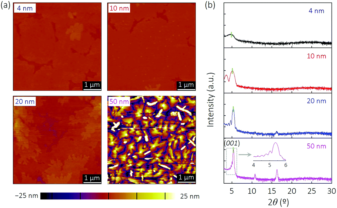 | ||
| Fig. 1 DNTT film property analysis: (a) AFM images of 4 nm, 10 nm, 20 nm and 50 nm-thick slow-evaporated DNTT films; (b) the corresponding XRD patterns of DNTT films with various thicknesses on a logarithmic scale. | ||
As the access resistance influences the charge injection and transport in the bulk region, 20 nm-thick slow-evaporated DNTT films were chosen to fabricate OFETs with various channel lengths (L varies from 50 to 350 μm) to investigate the electrical properties and the corresponding charge transport in the active channels. Fig. 2a–e show the typical transfer (in both saturation and linear regimes) and output characteristics of a DNTT-based transistor device (L = 100 μm). This device yielded a high field-effect mobility of 2.04 cm2 V−1 s−1, a large on/off ratio of ∼106 (in the saturation regime) and negligible hysteresis, indicating an excellent DNTT/SiO2 interface with low trap states. The reliability factors in the saturation and linear regimes were 81.5% and 91.4%, respectively.21 A nearly linear increase in the small range of drain voltage (VD = 0 to −10 V) in the output curves was clearly observed, suggesting that the contact resistance is relatively small compared with the channel resistance of DNTT OFETs (more discussion is shown in Note S1, ESI†). In addition, the OFETs with various channel lengths exhibited decreasing carrier mobility with increasing channel length (Fig. 2f). We attributed this trend to the existence of domain boundaries in the DNTT films (as shown in Fig. 1a) although possessing high crystallinity. The transistors with L < 100 μm could be considered as single-crystal-like-OFET devices where the DNTT films contained fewer domains and thus possessed a higher carrier mobility.13,22,23
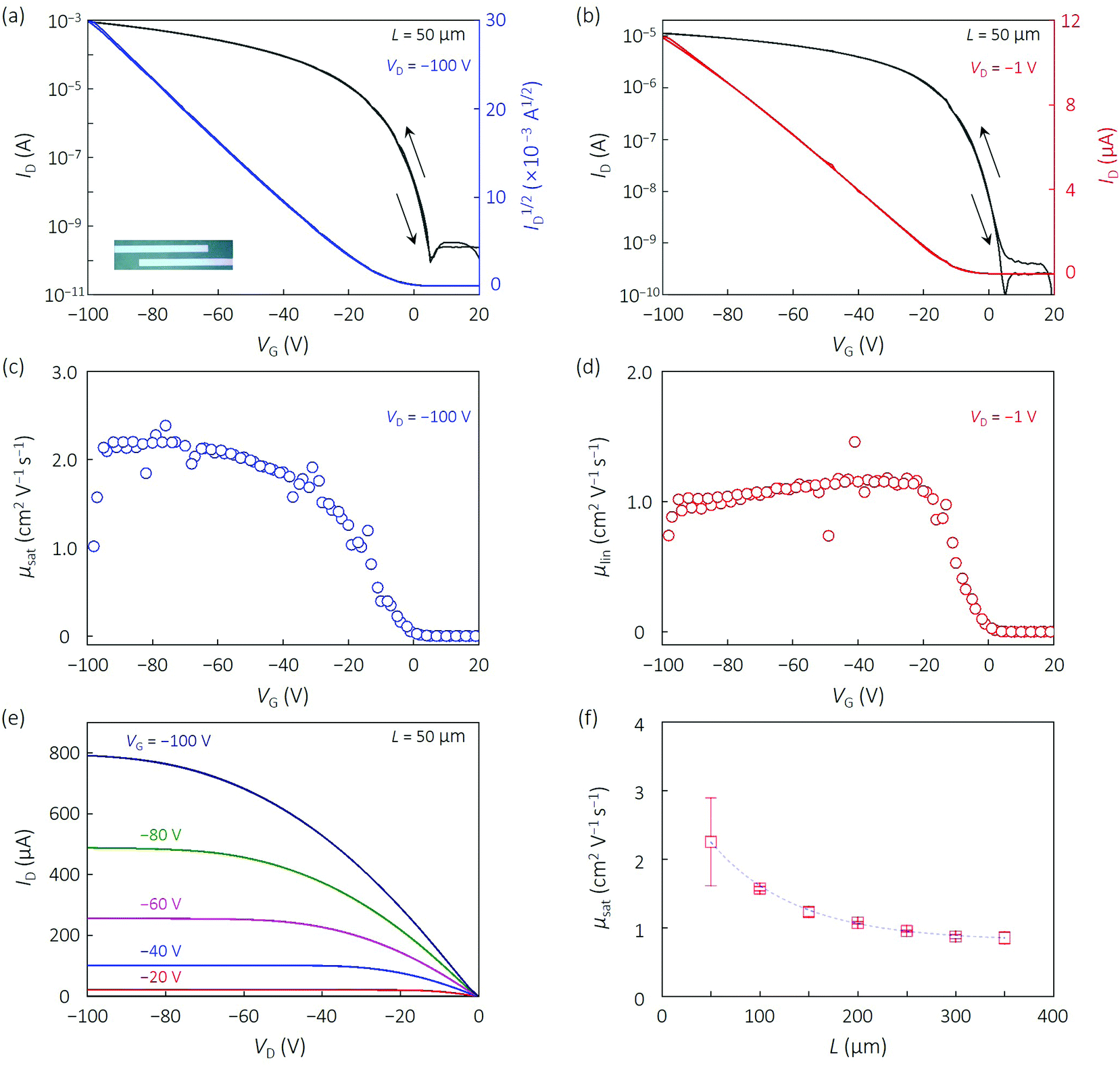 | ||
| Fig. 2 Typical electrical properties of slow-evaporated DNTT transistors. Transfer characteristics at a drain voltage of VD = −100 V (a, saturation regime) and −1 V (b, linear regime) for OFETs based on the 20 nm-thick DNTT films. The reliability factors in the saturation and linear regimes were 81.5% and 91.4%, respectively. (c) Saturation mobility and (d) linear mobility plotted as a function of gate voltage. (e) Its corresponding output characteristics. VG was changed from 0 to −100 V with a step of −20 V. The channel length (L) and width (W) are 50 μm and 500 μm, respectively. (f) Relationship between the channel length and carrier mobility. | ||
To study the charge transport behavior in the slow-evaporated DNTT-based transistors, we characterized the transfer curves by temperature-dependence measurements (Fig. 3a). A small shift in the drain current and threshold voltage along with the decreasing temperature is observed. As shown in Fig. 3b, the extracted carrier mobilities from DNTT-based OFETs (L = 50 μm) exhibited a nearly temperature-independent (∂μ/∂T = 0) trend while devices with L > 100 μm exhibited a positive carrier mobility–temperature dependence (∂μ/∂T > 0) (Fig. S2, ESI†). The L-dependent charge transport was caused by the domain boundaries existing in long-L DNTT OFETs, where the transport was temperature-dependent and thermally activated.24 Based on the Marcus theory and polaron theory in low-mobility organic materials, the charge carriers in channels generally transfer through hopping where the carrier mobility (μ is calculated without any under- or overestimation) exhibits a positive dependence on the temperature (that is ∂μ/∂T > 0).24 Besides, the temperature-independent carrier mobility has also been observed in single-crystal DNTT-based OFETs while the deep physical mechanism is still unclear.13 For comparison, we further fabricated the OFETs based on the fast-evaporated 20 nm-thick DNTT films and evaluated the carrier mobility at various temperatures (for the film deposition details, see the Experimental section). Although the room-temperature carrier mobilities of OFETs utilizing the slow- and fast-evaporated DNTT films were approximately identical (1.93 ± 0.35 and 1.86 ± 0.42 cm2 V−1 s−1, respectively) (Fig. S3, ESI†), obvious hysteresis was seen in the fast-evaporated devices, indicating a large number of trap states existing in the semiconducting channels. More electrical parameters are summarized in Table S1, ESI.† We further calculated the maximum density of the traps (Ntrap) resulting from the dielectric property and defects in semiconductors by using SS through the following equation: Ntrap = Ci(SS × e/(kBTln![[thin space (1/6-em)]](https://www.rsc.org/images/entities/char_2009.gif) 10) − 1)/e2, where Ci is the capacitance per unit area of the dielectric layer, e is the elementary charge, and kB is the Boltzmann constant. The Ntrap value for the slow-evaporated DNTT devices is ∼2.56 × 1012 cm−2; this value is reduced significantly from ∼ 4.62 × 1012 cm−2 for the fast-evaporated DNTT devices. Note that the initial 4 nm-thick DNTT films of both samples, working as the active channel at the DNTT/SiO2 interface, were optimized and deposited by slow evaporation. Therefore, the Ntrap reduction mainly resulted from the access region in the semiconductor bulk. Generally, trap states in organic semiconductors go against the smooth charge transport and device performance. The activated charge transport of fast-evaporated DNTT-based OFETs was observed as shown in Fig. 3b. The carrier mobility shows an obvious decreasing trend at lower temperatures (Fig. S4, ESI†).15
10) − 1)/e2, where Ci is the capacitance per unit area of the dielectric layer, e is the elementary charge, and kB is the Boltzmann constant. The Ntrap value for the slow-evaporated DNTT devices is ∼2.56 × 1012 cm−2; this value is reduced significantly from ∼ 4.62 × 1012 cm−2 for the fast-evaporated DNTT devices. Note that the initial 4 nm-thick DNTT films of both samples, working as the active channel at the DNTT/SiO2 interface, were optimized and deposited by slow evaporation. Therefore, the Ntrap reduction mainly resulted from the access region in the semiconductor bulk. Generally, trap states in organic semiconductors go against the smooth charge transport and device performance. The activated charge transport of fast-evaporated DNTT-based OFETs was observed as shown in Fig. 3b. The carrier mobility shows an obvious decreasing trend at lower temperatures (Fig. S4, ESI†).15
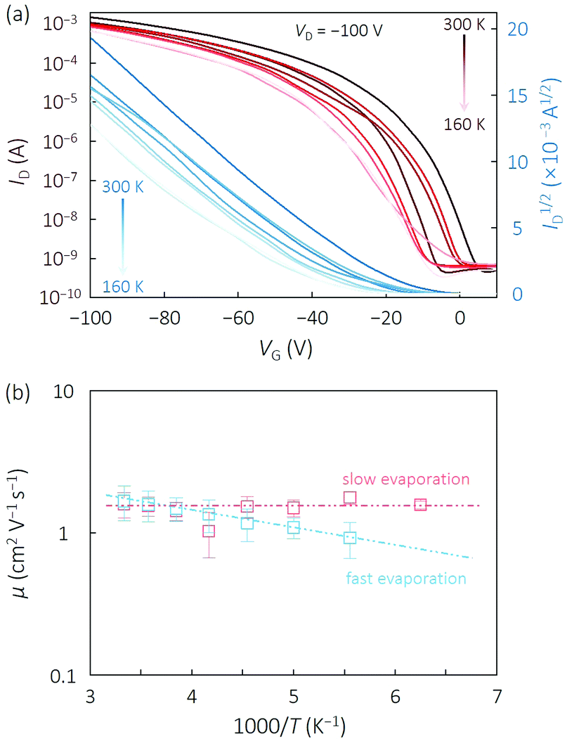 | ||
| Fig. 3 Temperature dependence of the electrical properties of slow- and fast-evaporated BGTC DNTT transistors. Two-probe measurements were used in the analysis of carrier mobility. (a) Typical transfer characteristics of a slow-evaporated DNTT transistor at various temperatures. The channel length and width are 50 μm and 500 μm, respectively. (b) Field-effect mobility of slow- and fast-evaporated DNTT transistors as a function of temperature. | ||
As the DNTT films at the semiconductor/dielectric interface (initial 4 nm) possessed the same crystalline properties and molecular packing, we considered that the difference of the observed charge transport in both samples was caused by other factors, e.g. contact resistance (RC). Thus, we further evaluated the RC value of the slow- and fast-evaporated DNTT OFETs using the transmission line method (TLM). The RC values of both devices were extracted from the transfer curves in the linear region (Fig. S5, ESI†) and are shown in Fig. 4. We found that the RC value of the slow-evaporated device is lower than that of the fast-evaporated counterparts at high gate voltages (∼51 kΩ and 75 kΩ at VG = −100 V, respectively). Since the fabrication of OFETs and the deposition of DNTT films were carried out using the same process but different evaporation rates, the reduction in contact resistance was attributed to the upper DNTT film property (that is, the semiconductor bulk).25,26 Note that RC largely varies with VG and stabilizes at high values of gate voltage (VG), which is in part caused by trap filling in the access region.11,27,28 Trap states were mainly introduced during the DNTT film deposition and the contact metal formation, and could be filled gradually upon elevating the Fermi level, namely, by increasing VG.
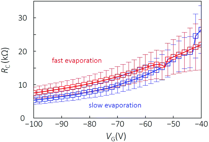 | ||
| Fig. 4 R C of the OFETs based on slow- and fast-evaporated DNTT films. The RC values of the slow- and fast-evaporated DNTT OFETs were evaluated by the TLM. The channel length varies from 50 to 350 μm. Error bars represent the uncertainty in fitting from the TLM. | ||
These two contact resistances are directly tuned by the thermal evaporation rates, which lead to different film crystallinity and molecular packing. Therefore, we compared the XRD patterns of the DNTT films deposited by the slow and fast evaporation and found that the (001) peak position shows a negligible shift from 2θ = 5.43° for the fast-evaporated sample to 2θ = 5.31° for the slow-evaporated sample (Fig. 5a). Furthermore, the corresponding d-spacing values for these two samples are 16.3 and 16.6 Å, indicating more tilted molecules or disorders (such as structural defects) on average in the fast-evaporated sample. For the (001) peaks fitted by the Gaussian function (the inset in Fig. 5a), the slow-evaporated film exhibits a considerably smaller full width at half-maximum (decreasing from 0.47° to 0.38°) compared to that of the fast-evaporated film. These results indicate that the slow-evaporated DNTT film exhibits better crystallinity and a larger crystallite size compared to the fast-evaporated DNTT film. In addition, the (001) peak intensity of slow-evaporated DNTT films is nearly one order higher than that of fast-evaporated samples. As shown in Fig. 5a, no fringes can be observed in the fast-evaporated DNTT films, while clear Laue fringes in addition to the (001) Bragg peak are observed in the slow-deposited sample. More detailed information about the XRD data is shown in Fig. S6, ESI.† These observations afforded valid evidence that the slow-evaporated DNTT films exhibited well-defined layered molecular packing of the whole measured area.
 | ||
| Fig. 5 XRD and UPS analyses. (a) XRD patterns on a logarithmic scale of (top) slow- and (bottom) fast-evaporated 20 nm-thick DNTT films. The peaks at 2θ = 5.31° and 5.43° in these samples both correspond to the (001) peak. The inset shows the Gaussian fittings of the (001) peaks. (b) UPS spectra near the cutoff for secondary electron emission (left) and near the HOMO edge (right) for (blue) slow- and (red) fast-evaporated DNTT films. | ||
Generally, the orientation of organic molecules affects the interface dipoles and overlapping of molecular orbitals, which will eventually affect their energy levels, such as the highest occupied molecular orbital (HOMO) and the work function (WF); hence, the binding energies of DNTT films deposited via slow and fast processes were characterized through the ultraviolet photoelectron spectroscopy measurements (UPS) (Fig. 5b). Both the HOMO and WF of this interfacial layer exhibited slight shifts (∼0.1 eV), indicating that the fast-evaporated DNTT films contain tilted molecules, especially in the upper few layers. Thus, we proposed the molecular packing of DNTT molecules in the upper layers depicted in the insets (Fig. 5b).29 The disordered packing in the c-axis resulted in an easily blocked transport pathway. Thus, the corresponding large access resistance was the main reason for the difference in the observed charge transport between these samples. The contact resistance also exhibited a temperature-dependent feature.11,30
Conclusions
In summary, the carrier mobility in DNTT-based OFETs showed different features due to the different evaporation processes for DNTT films, especially the semiconductor bulk regime. The μFET value in slow-evaporated devices exhibited a temperature-independent trend while the fast-evaporated samples showed an obvious character of ∂μ/∂T > 0. Our investigations revealed that such a difference was due to the crystalline property of DNTT films in the access region, where highly ordered molecular packing in the c-axis effectively facilitated the charge transport in this direction. The transition of the observed temperature–carrier mobility dependence could be modulated by the access resistance originating from the molecular packing and film crystallinity. Since the transfer integrals in the c-axis were much lower than those the in ab-plane and the corresponding transport in this direction was still dominated by the hopping mode, the reduction of contact resistance could further contribute to the optimization of the device fabrication and charge transport analysis. This work demonstrated the effect of the access region on the study of charge transport and device physics in the active channels in OFETs. We believe that an accurate analysis of the relationship between carrier mobility and the corresponding temperature–carrier mobility will benefit the whole study of charge transport in OFETs. One potential strategy to eliminate this effect is to utilize two-dimensional organic semiconductors and realize a nearly ohmic contact or tunneling carrier injection and extraction at the semiconductor/electrode interface in OFET devices.Experimental
Fabrication of DNTT films
The 300 nm-thick SiO2/Si substrates were sequentially cleaned by sonication in acetone and isopropanol for 5 min each. The p-type organic semiconductor DNTT was purchased from Aldrich and used without further purification. The fast-evaporated DNTT films were prepared in two steps: the initial 4.0 nm-thick film was evaporated at a slow rate (∼0.0017 Å s−1), and then the additional 6 nm, 16 nm and 46 nm-thick films were sequentially evaporated at a fast rate (∼0.1 Å s−1). For slow-evaporated films, all DNTT films with various thicknesses were deposited on SiO2/Si substrates by slow thermal evaporation (∼0.0017 Å s−1) with a base pressure of 10−4 Pa.Characterization of DNTT films
The XRD measurements (Bruker AXS K. K.) using Cu Kα source X-rays were used to evaluate the DNTT films. The binding energy was characterized by the UPS (Kratos AXIS ULTRA HAS He-Iα = 21.22 eV). The binding energy for UPS was calibrated by measuring the Fermi edge (EF = 0 eV) on a clean Au surface (for more details see ref. 15). The surface morphology was analyzed by the AFM (Asylum Research MFP-3D) in tapping mode.Fabrication and electrical measurements of OFETs
Bottom-gate top-contact (BGTC) OFETs were fabricated with the defined DNTT films through a shadow mask. All DNTT films used in OFETs were 20 nm. Subsequently, 80 nm-thick Au electrodes were thermally evaporated on the DNTT films at a rate of ∼0.1 Å s−1. Electrical measurements were performed utilizing a Keithley 4200 semiconductor parameter analyzer in a closed-cycle cryogenic probe station with a base pressure of 10−4 Pa. During temperature-dependent measurements, the temperature decreased at a slow rate of 0.2 K min−1, avoiding damages to DNTT films. The saturation region equation [ID = μsatCi(W/2L)(VG − VT)2] and the linear region equation [ID = μlinCi(W/L)(VG − VT)/VD] were applied for carrier mobility calculations.Conflicts of interest
There are no conflicts to declare.Acknowledgements
Y. L. and Q. W. conceived the idea and initiated and supervised the work. Q. W. designed, implemented, and optimized the deposition and characterization of DNTT films, device fabrication and electrical measurements. The manuscript was written through contributions of all authors. All authors have approved the final version of the manuscript. This work was supported by the China Postdoctoral Innovation Program, China Postdoctoral Science Foundation under Grant No. 2019M651782, the NSFJS under Grant No. BK20170075, and the NSFC under Grant No. 61774080 and 51861145202.References
- X. Zhang, H. Dong and W. Hu, Adv. Mater., 2018, 30, 1801048 CrossRef PubMed.
- T. Hasegawa and J. Takeya, Sci. Technol. Adv. Mater., 2009, 10, 024314 CrossRef PubMed.
- H. Sirringhaus, Adv. Mater., 2014, 26, 1319–1335 CrossRef CAS PubMed.
- S. Fratini, D. Mayou and S. Ciuchi, Adv. Funct. Mater., 2016, 26, 2292–2315 CrossRef CAS.
- Y. Okada, K. Sakai, T. Uemura, Y. Nakazawa and J. Takeya, Phys. Rev. B: Condens. Matter Mater. Phys., 2011, 84, 245308 CrossRef.
- X. Ren, M. J. Bruzek, D. A. Hanifi, A. Schulzetenberg, Y. Wu, C. H. Kim, Z. Zhang, J. E. Johns, A. Salleo, S. Fratini, A. Troisi, C. J. Douglas and C. D. Frisbie, Adv. Electron. Mater., 2017, 3, 1700018 CrossRef.
- S. Fratini and S. Ciuchi, Phys. Rev. Lett., 2009, 103, 266601 CrossRef CAS PubMed.
- A. Troisi and G. Orlandi, Phys. Rev. Lett., 2006, 96, 086601 CrossRef PubMed.
- C. Liu, K. Huang, W. T. Park, M. Li, T. Yang, X. Liu, L. Liang, T. Minari and Y. Y. Noh, Mater. Horiz., 2017, 4, 608–618 RSC.
- S. M. Sze, Physics of Semiconductor Devices, John Wiley & Sons, Inc., New York, 1981 Search PubMed.
- P. V. Pesavento, R. J. Chesterfield, C. R. Newman and C. D. Frisble, J. Appl. Phys., 2004, 96, 7312–7324 CrossRef CAS.
- P. V. Pesavento, K. P. Puntambekar, C. D. Frisbie, J. C. McKeen and P. P. Ruden, J. Appl. Phys., 2006, 99, 094504 CrossRef.
- W. Xie, K. Willa, Y. Wu, R. Häusermann, K. Takimiya, B. Batlogg and C. D. Frisbie, Adv. Mater., 2013, 25, 3478–3484 CrossRef CAS PubMed.
- H. Sun, Q. Wang, Y. Li, Y. F. Lin, Y. Wang, Y. Yin, Y. Xu, C. Liu, K. Tsukagoshi, L. Pan, X. Wang, Z. Hu and Y. Shi, Sci. Rep., 2014, 4, 7227 CrossRef CAS PubMed.
- Q. Wang, S. Jiang, L. Qiu, J. Qian, L. K. L. K. Ono, M. R. M. R. Leyden, X. Wang, Y. Y. Shi, Y. Zheng, Y. Qi and Y. Li, ACS Appl. Mater. Inter., 2018, 10, 22513–22519 CrossRef CAS PubMed.
- M. C. Jung, M. R. Leyden, G. O. Nikiforov, M. V. Lee, H. K. Lee, T. J. Shin, K. Takimiya and Y. Qi, ACS Appl. Mater. Interfaces, 2015, 7, 1833–1840 CrossRef CAS PubMed.
- Q. Wang, E. J. Juarez-Perez, S. Jiang, L. Qiu, L. K. Ono, T. Sasaki, X. Wang, Y. Shi, Y. Zheng, Y. Qi and Y. Li, J. Phys. Chem. Lett., 2018, 9, 1318–1323 CrossRef CAS PubMed.
- S. Jiang, J. Qian, Y. Duan, H. Wang, J. Guo, Y. Guo, X. Liu, Q. Wang, Y. Shi and Y. Li, J. Phys. Chem. Lett., 2018, 9, 6755–6760 CrossRef CAS PubMed.
- T. Yokota, T. Kajitani, R. Shidachi, T. Tokuhara, M. Kaltenbrunner, Y. Shoji, F. Ishiwari, T. Sekitani, T. Fukushima and T. Someya, Nat. Nanotechnol., 2018, 13, 139–144 CrossRef CAS PubMed.
- T. Hamai, S. Arai, H. Minemawari, S. Inoue, R. Kumai and T. Hasegawa, Phys. Rev. Appl., 2017, 8, 054011 CrossRef.
- H. H. Choi, K. Cho, C. D. Frisbie, H. Sirringhaus and V. Podzorov, Nat. Mater., 2017, 17, 2–7 CrossRef PubMed.
- A. Hamaguchi, T. Negishi, Y. Kimura, Y. Ikeda, K. Takimiya, S. Z. Bisri, Y. Iwasa and T. Shiro, Adv. Mater., 2015, 27, 6606–6611 CrossRef CAS PubMed.
- S. G. J. Mathijssen, E. C. P. Smits, P. A. Van Hal, H. J. Wondergem, S. A. Ponomarenko, A. Moser, R. Resel, P. A. Bobbert, M. Kemerink, R. A. J. Janssen and D. M. D. Leeuw, Nat. Nanotechnol., 2009, 4, 674–680 CrossRef CAS PubMed.
- M. Yamagishi, J. Soeda, T. Uemura, Y. Okada, Y. Takatsuki, T. Nishikawa, Y. Nakazawa, I. Doi, K. Takimiya and J. Takeya, Phys. Rev. B: Condens. Matter Mater. Phys., 2010, 81, 161306 CrossRef.
- M. Marinkovic, D. Belaineh, V. Wagner and D. Knipp, Adv. Mater., 2012, 24, 4005–4009 CrossRef CAS PubMed.
- D. Natali, J. Chen, F. Maddalena, F. García Ferré, F. Di Fonzo and M. Caironi, Adv. Electron. Mater., 2016, 2, 1600097 CrossRef.
- I. Yagi, K. Tsukagoshi and Y. Aoyagi, Appl. Phys. Lett., 2004, 84, 813–815 CrossRef CAS.
- R. J. Chesterfield, J. C. McKeen, C. R. Newman, C. D. Frisbie, P. C. Ewbank, K. R. Mann and L. L. Miller, J. Appl. Phys., 2004, 95, 6396–6405 CrossRef CAS.
- S. Duhm, G. Heimel, I. Salzmann, H. Glowatzki, R. L. Johnson, A. Vollmer, J. P. Rabe and N. Koch, Nat. Mater., 2008, 7, 326–332 CrossRef CAS PubMed.
- S. D. Wang, T. Minari, T. Miyadera, K. Tsukagoshi and Y. Aoyagi, Appl. Phys. Lett., 2007, 91, 203508 CrossRef.
Footnote |
| † Electronic supplementary information (ESI) available. See DOI: 10.1039/d0ma00530d |
| This journal is © The Royal Society of Chemistry 2020 |