
 Open Access Article
 This Open Access Article is licensed under a Creative Commons Attribution-Non Commercial 3.0 Unported Licence
Ambient condition-processing strategy for improved air-stability and efficiency in mixed-cation perovskite solar cells†
Ivy M.
Asuo
 ab,
Dawit
Gedamu
b,
Nutifafa Y.
Doumon
ac,
Ibrahima
Ka
a,
Alain
Pignolet
a,
Sylvain G.
Cloutier
*b and
Riad
Nechache
*a
ab,
Dawit
Gedamu
b,
Nutifafa Y.
Doumon
ac,
Ibrahima
Ka
a,
Alain
Pignolet
a,
Sylvain G.
Cloutier
*b and
Riad
Nechache
*a
aINRS – Centre Énergie Matériaux Télécommunications, 1650 Boul. Lionel Boulet, Varennes (QC), J3X 1S2, Canada. E-mail: nechache@emt.inrs.ca
bÉcole de Technologie Supérieure (ÉTS), Department of Electrical Engineering, 1100 rue Notre-Dame Ouest, Montréal (QC), H3C 1K3, Canada. E-mail: SylvainG.Cloutier@etsmtl.ca
cPhotophysics and Optoelectronics, Zernike Institute for Advanced Materials, University of Groningen, Nijenborgh 4, NL-9747 AG, Groningen, The Netherlands
First published on 27th July 2020
Abstract
Fabrication of efficient halide perovskite solar cells under ambient conditions and their stability remain a challenge due to the sensitivity of halide perovskites to moisture, oxygen, light, and temperature. Thus, there is a strong demand and interest to develop a method for fabricating perovskite solar cells with long-term stability and even better, such a fabrication method under ambient conditions. To this end, we use a chemical synthesis method and a solvent engineering technique to optimize halide perovskite thin film deposition in an ambient environment. We obtained pinhole-free films composed of large crystal grains and high crystal quality that result in excellent optoelectronic properties of the halide perovskite. We also report a low trap-density in the order of 1015 cm−3 for the polycrystalline perovskite thin film. Moreover, with an n–i–p solar cell structure, a maximum power conversion efficiency of ∼20.3% with excellent stability in ambient air (25–55%RH) for more than ten months of storage (>7000 hours) is achieved. The optimized solar cell without encapsulation retained ∼80% of its initial performance after ten months of storage with a T80 of ∼5035 hours. Our findings suggest that the performance and stability of the perovskite solar cells are highly dependent on the device architecture, grain morphology, trap density, and carrier mobility in the device before and after storage.
Introduction
Halide perovskite photovoltaic cells have generated tremendous attention due to their promising material properties and low-temperature processing from solution precursors. Halide perovskites have great potential as an alternative material for solar cells with a high power conversion efficiency (PCE) of up to 25.2%.1 Their effective photon absorption,2 low exciton binding energy,3 and tunable bandgap (1.5–2.2 eV)4 are advantageous for applications such as light-emitting diodes (LEDs),5–7 photovoltaics (PVs)8–10 and photodetector devices.11–13 Albeit the remarkable progress from the past few years, organic–inorganic halide perovskite (OIHP) processing and its stability under ambient conditions remain an open challenge towards commercialization. The shelf-lifetime of OIHP, especially CH3NH3PbI3-based devices under ambient air conditions, is very short,14 and their performances decrease rapidly due to the extrinsic and intrinsic instabilities of the halide perovskites.15–17 For these reasons, OIHP material synthesis and thin film fabrication are usually conducted under an inert atmosphere. The use of glove box facilities is a substantial impediment for large scale OIHP-based device manufacturing.18 Thus, a halide perovskite material processable under ambient conditions, offering long-term stability and high performance, is currently in high demand. Recently, several methods have been explored to address this challenge through synthesis and structure optimization19,20 to achieve stable and compact halide perovskite thin films. The process of obtaining compact and large crystal grain thin film on a given substrate is challenging but crucial for high-performance devices.21 For optimum device performances, the ideal perovskite film should be pinhole-free, composed of large crystal grains, and have a smooth surface22 with fewer grain boundaries.23,24 Therefore, recent investigations focus directly or indirectly on achieving high-quality perovskite films using a single,25 double,26 or triple cation27 system in order to increase both performance and stability of the devices. However, the ambient environment accelerates the degradation of OIHP of even high-quality perovskite films by promoting the rapid decomposition of OIHP material into optically-inert constituents such as PbI2.14 Notwithstanding, a recent report proposed a triple-cation system with high efficiency and relatively good PV stability performance under continuous illumination27 and thermal stress.28 Yet, all the material synthesis, device fabrication, and testing were performed under an inert atmosphere.27,28Here, we describe a synthesis and processing technique entirely performed under ambient conditions. In addition, we characterize the devices only under ambient conditions for their efficiency and air-stability. We focus on tailoring perovskite grain size and crystal quality by using an ionic additive, lead thiocyanate (Pb(SCN)2), and a solvent–antisolvent (ethanol and chlorobenzene) engineering technique for the mixed-cation perovskite. The use of ethanol and chlorobenzene for solvent treatment is known to promote the nucleation and growth of large grains and a good crystallization of the perovskite.29,30 Ethanol, in particular, contributes to the dissolution of the remnant MAI, FAI, and MABr, since these organic precursors of the perovskite are soluble in ethanol. Chlorobenzene, an antisolvent for the perovskite, is used for inducing the fast precipitation of the perovskite film, resulting in the growth of smooth, well-crystallized, and large grain perovskite films. The literature also advocates that when inserted into perovskite precursors, pseudohalide additives such as Pb(SCN)2 increase the tolerance of perovskite-based solar cells to relative humidities (RH%) of above 70%31,32 while conserving their microstructural properties. It also reduces radiative and non-radiative losses, thereby improving the device performance.33 The mixing of Pb(SCN)2 with CH3NH3PbI3 leads to the replacement of I− by SCN− in the precursor. Since SCN− works similarly as I− (the halide), it is thus termed a pseudohalide.
The presence of thiocyanate (SCN−) anions in OIHP films does not upset the crystallographic structure of CH3NH3PbI3, since it has a similar ionic radius (∼0.217 nm) to iodine ions, I− (∼0.220 nm).34 Pb(SCN)2 has been used as the precursor material or additive to synthesize pseudohalide perovskites for the improvement in microstructural and optical properties of CH3NH3PbI3. Over the years, Pb(SCN)2-doping of single35,36 or double cation26,37 perovskites has been studied towards large-grain and efficient perovskite devices.2,38 Most of the studies on pseudohalide perovskites (some processed under inert environments) indicated that the addition of pseudohalide could enhance the moisture-resistivity and quality of perovskite thin films.39 In our work, we adequately implemented Pb(SCN)2 in the triple cation perovskite in combination with a solvent–antisolvent precipitation technique under ambient conditions, therefore contributing not only towards improving the performance of our devices but also towards a much simple process, paving the way towards upscaling and applications. Using our optimized processing method, we produce compact perovskite films and large crystal grains with passivated grain boundaries. The perovskite thin-films are then used to fabricate n–i–p-heterostructured solar cells. Very importantly, the whole fabrication and characterization process is carried out in ambient air (25–55% RH). As a result, perovskite solar cells with high efficiency (∼20.3%), and excellent long-term air-stability of more than ten months (and a T80 of ∼5035 hours) are achieved, a valuable point to be highlighted. In addition, trap-state densities and the charge transport mechanisms before and after device degradation have been evaluated through the space charge limited current (SCLC) method to understand the physical source of the degradation. The ability to develop our perovskite solar cells under ambient conditions coupled with their high-performance paves the way towards industrial production of low-cost, efficient, and long-term stable solar cells.
Results and discussions
A one-step solution process is used to synthesize the mixed-halide perovskite films. Details of the fabrication processes are presented in the Experimental section. The perovskite samples with and without the additive are labeled SOL-x and SOL-0, respectively. The main difference between SOL-0 and SOL-x (where x is the weight percent of the additive) devices comes from the addition of thiocyanate anions (SCN), derived from Pb(SCN)2, to the precursor solutions before the deposition of the thin films. A range of weight percentages of the additive from 0–11 wt% was used to determine the optimum proportion of SCN to achieve the best performance of the solar cells, as shown in Fig. S1 (ESI†). The optimum concentration of 5.8 wt% of the additive has been adopted for further investigations. That is, the devices with SOL-5.8 have been fabricated using a precursor solution containing approximately 5.8 wt% of the Pb(SCN)2 additive.The top-view of the scanning electron microscopy (SEM) images of the SOL-0 and SOL-5.8 perovskite films are shown in Fig. 1(a) and (b), while Fig. S2 (ESI†) shows the considered perovskite films without and with the complete concentration range of the ionic additive studied. In general, SOL-x films seem to show better morphology. For instance, the SOL-0 film shows compact morphology and consists of fine grains with an average size of ∼200 nm, while the SOL-5.8 film, remarkably, shows very dense, pinhole-free, and large grains >2 μm in size. Also, the micrograph of the SOL-5.8 film shows grain boundaries (GBs) with a brighter contrast between the grains upon the addition of Pb(SCN)2, as shown in Fig. 1(b) and (b-1). Such addition leads to an increased crystal size, reduced traps, and improved device stability of the perovskite films. The mechanisms for enlarged grains have been proposed to originate from lower Gibbs free energy for the nucleation due to the beneficial effect of the incorporated SCN− ion.37,40 Furthermore, during the perovskite film formation, there could be a reaction between CH3NH3+ cations and SCN−anions, leading to the formation of CH3NH2 gas.39,41 The CH3NH2 gas is known to increase the grain size and the crystalline quality of the perovskite thin films. This could be the reason behind the grain enlargement of our thin films. Moreover, in a previous report, we demonstrated that solvent–antisolvent treatment of perovskite films also results in larger grains.30 These two phenomena led to fewer and passivated GBs, resulting in the reduced recombination and increased crystallite size.42,43
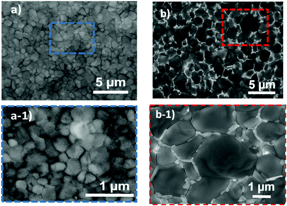 | ||
| Fig. 1 SEM images of the perovskite films without the additive SOL-0 (a and a-1) and with 5.8 wt% of the additive (SOL-5.8) (b and b-1). | ||
The X-ray diffraction (XRD) patterns acquired and shown in Fig. 2(a) and (b) exhibit strong and sharp peaks matching the tetragonal structure of the halide perovskites, in agreement with previous reports.27,30 These XRD spectra also demonstrate that, since there is no observable peak at ∼12.7° in both spectra, the observed white regions at the grain boundaries are not predominantly PbI2, but are rather the Pb-, I- and S-rich regions, as shown by the energy-dispersive X-ray spectroscopy (EDS) spectra and mapping images (Fig. S3, ESI†) and by the Auger spectra (see Fig. S4(c)–(e), ESI†). In general, the mechanism of formation of the white regions at the GBs instigates from a crystallization point of view. We observe that increasing the volume ratio of added ethanol (above 50%) to chlorobenzene for the solvent treatment results in the enhancement of the PbI2 peak (figure not shown here), while keeping it below that threshold results in no strong PbI2 peaks. This explains why our optimum (SOL-5.8) films exhibited no PbI2 peaks on the XRD pattern. Fig. S3 (ESI†) depicts the presence of all the major elemental components in the perovskite films. The elemental composition measurement of the perovskite films using EDS is challenging since the emission lines of Pb and S are very close and overlap in the spectrum (Pb: Mα1 = 2.346 keV and S: Kα1 = 2.308 keV). Therefore, Auger electron spectroscopy (AES) was also used to determine the chemical composition of the films. As shown in Fig. S4c (ESI†), the reference sample (SOL-0) displays the presence of peaks corresponding to Pb, I, and C. The spectrum for the dark region (1) of the SOL-5.8 sample is similar to that of the SOL-0 sample (Fig. S4d, ESI†). We note that besides Pb and I, sulfur is also present at the GBs (Fig. S4e, ESI†) with higher Pb intensity. In brief, the characterization reveals that the bright regions at the GBs are the Pb-, I-, and SCN−-rich phases. Generally, the presence of excess Pb2+ at the grain boundaries is beneficial and has an impact on charge-carrier injection, hysteresis, and the overall device performance of PSCs.44 Thus, we show that passivation of the GBs through the systematic introduction of Pb(SCN)2 and the solvent–antisolvent treatment can effectively increase the grain size, while avoiding the formation of excessive PbI2, and hence improve the performance of the solar cells.
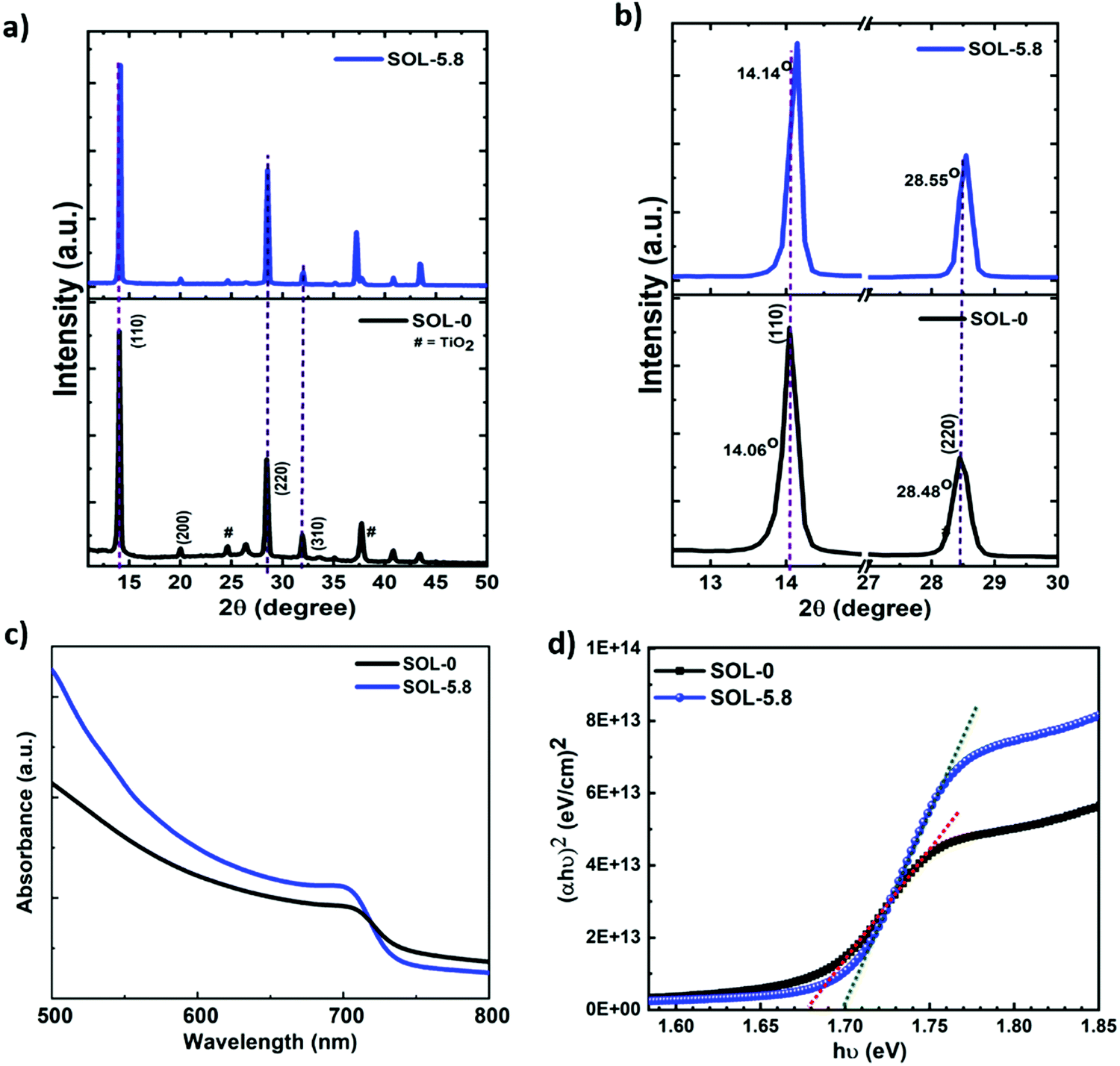 | ||
| Fig. 2 XRD spectra of (a) the prepared perovskite films and (b) magnified plots of the (110) and (220) peaks in (a). (c) UV-vis absorption spectra and (d) Tauc plots obtained from the absorption spectra for the SOL-0 and SOL-5.8 samples. | ||
Furthermore, the effect of the additive on the XRD peak positions is also revealed in Fig. 2(b). The SOL-5.8 films show better crystallinity compared to the SOL-0 films as shown by the peak intensities and their derived full width at half maximum (FWHM) values. The former shows more than a four-fold increase in intensity as compared to the latter (see Fig. S5a, ESI†). The peaks associated with (110) and (220) planes of the perovskite, slightly shift to higher angles. For instance, there is a shift from 14.06° to 14.14° for the (110) plane as a consequence of the ionic additive, indicative of a smaller lattice parameter.37 The FWHM obtained from the (110) peak shows that the SOL-5.8 films possess better crystallinity with a value of 0.17° with a crystallite size of 47.4 nm obtained from the Scherrer's equation.45 In contrast, the SOL-0 films exhibit a FWHM of 0.23° with a crystallite size of 34.6 nm. As such, the use of ionic additives and solvent treatment impacts the microstructural properties of the halide perovskites. We further characterized the optical properties of the perovskite films using UV-vis absorption spectroscopy. In Fig. 2(c), the absorption spectra suggest excellent light-harvesting properties with a broad and well-defined absorption band. The corresponding band gaps estimated from the Tauc plots are 1.68 eV and 1.7 eV for SOL-0 and SOL-5.8 perovskite films, respectively (Fig. 2(d)). In brief, we indeed improve the microstructural properties of the perovskite material, which are crucial parameters for an efficient thin-film-solar cell device.
To evaluate the photovoltaic performance of the perovskite materials with and without additives, we fabricate both planar TiO2 and mesoporous TiO2 solar cells. The planar solar cells have an incorporated TiO2 blocking layer, also known as compact layer TiO2 (CL-TiO2), while the mesoporous solar cells have a Li-doped mesoporous TiO2 layer atop the TiO2 blocking layer (which we denote here as MP-TiO2). Fig. 3 presents the device architecture and the corresponding SEM cross-sectional image of the solar cells fabricated with the mesoporous TiO2 layer (See Fig. S5(b) and (c) for the planar configuration, ESI†). The device structure is a full-stack multilayered structure of the 3D perovskite solar cell (PSC), showing each layer and junctions. Our conventional device geometry comprises of FTO/TiO2/perovskite/spiro-OMeTAD/Au with a ∼500 nm thickness of the perovskite film (Fig. 3(b)). The schematic in Fig. 3(c) presents the energy band alignment of the respective layers in the solar cells and the charge extraction paths upon solar irradiation. It is worth emphasizing here that the complete device fabrication has been performed under ambient laboratory conditions (T = 20–25 °C, RH = 25–55%RH).
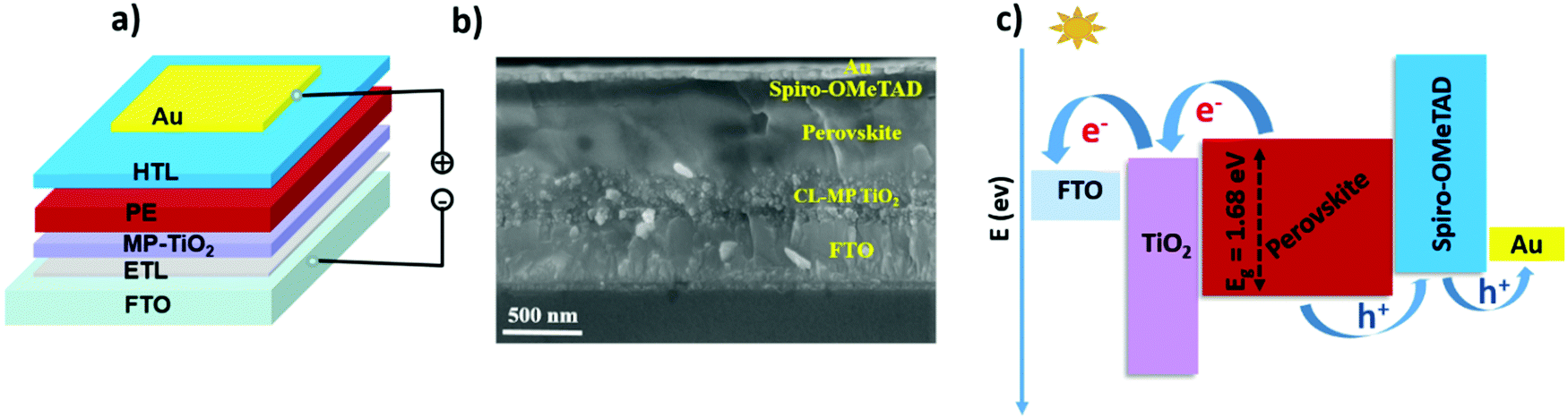 | ||
| Fig. 3 (a) Device configuration for: glass/FTO/TiO2/perovskite/spiro-OMeTAD/gold. FTO is the bottom electrode. The first layer, which is a compact or mesoporous TiO2 n-type material, acts as an electron transport layer (ETL). A p-type third layer of spiro-OMeTAD acts as the hole-transport layer (HTL). Gold acts as the counter electrode. (b) A cross-sectional SEM image of a mesoporous TiO2-based solar cell corresponding to each layer in (a). (c) The schematic diagram of the energy band alignment shows the charge transport mechanism upon illumination. | ||
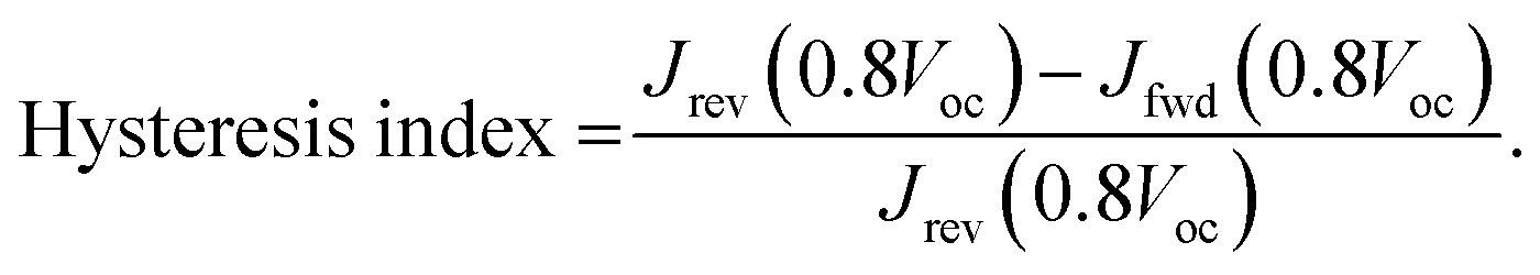
Fig. 4(a) shows the current density–voltage (J–V) characteristics of the different solar cell configurations. SOL-0-CL represents the device fabricated with the CL-TiO2 as ETL, while SOL-5.8-CL and SOL-5.8-MP are the devices fabricated with the CL-TiO2 layer and the CL-TiO2/MP-TiO2 double layer, respectively, as ETL. The photovoltaic parameters of the solar cells fabricated under similar conditions, including the short circuit current density (Jsc), open-circuit voltage (Voc), fill factor (FF), and PCE are summarized in Table 1. The PCE results indicate that, in general, the SOL-5.8-CL devices outperformed the SOL-0-CL devices (18.1% versus 10.97% for the best-performing cells). The sole use of the ionic additive resulted in an improvement of ∼64% in the PCE (also see Fig. S1, ESI†). Furthermore, the solar cells with the MP-TiO2 layer exhibit a higher FF with a slight increase in the PCE to 20.3% with moderate hysteresis in the J–V scan at 16 mV s−1 (Fig. 4(b)). From the cross-sectional SEM image in Fig. S5(c) (ESI†), the perovskite film has quite a large thickness variation, which may be a possible reason for the low PCEs for PSCs with the CL-TiO2 planar structure. The hysteresis index (HI) for our optimized perovskite device, as estimated from the equation reported by Kim et al.46 is 0.0022. The corresponding PCE and Jsc outputs of the optimized device under continuous illumination are as shown in Fig. 4(c). The statistical distributions of Jsc, Voc, FF, and PCE for our different solar cells, illustrated in Fig. S6 (ESI†), demonstrate good reproducibility.
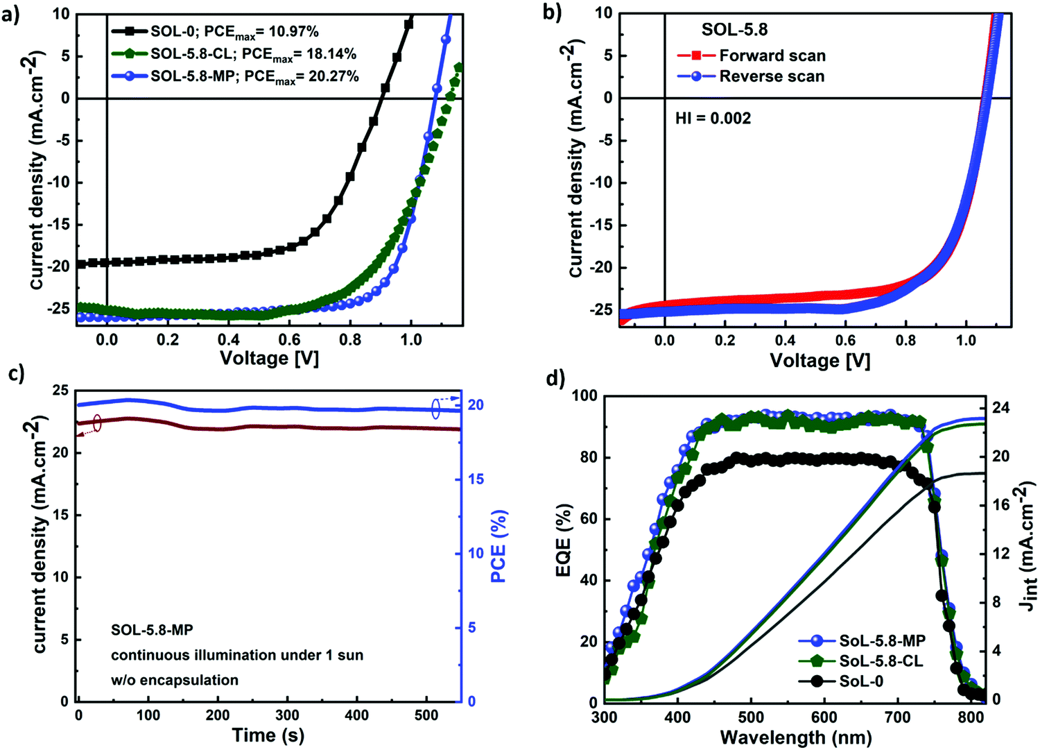 | ||
| Fig. 4 (a) Typical J–V curves, obtained under AM1.5 illumination, of solar cell devices fabricated on compact TiO2 (SOL-0-CL and SOL-5.8-CL) and mesoporous TiO2 (SOL-5.8-MP). The J–V characteristics were all measured in reverse scan directions. (b) J–V scans in both forward and reverse directions at a rate of 16 mV s−1 for SOL-5.8-MP. (c) Steady-state current density and PCE output under maximum voltage (0.9 V) for the optimized device. (d) EQE spectra and the calculated integrated current density (Jint) of the planar and mesoporous solar cells. | ||
| devices | J–V Par. | |||
|---|---|---|---|---|
| J sc (mA cm−2) | V oc (V) | FF (%) | PCE (%) | |
| Note: Par. = parameters.a 14 devices.b 16 devices.c 22 devices. | ||||
| SOL-0a | 19.50 (19.09 ± 0.56) | 0.91 (0.90 ± 0.01) | 61.9 (58.24 ± 4.85) | 11.0 (9.73 ± 0.65) |
| SOL-5.8-CLb | 24.98 (24.43 ± 0.35) | 1.13 (1.08 ± 0.03) | 64.3 (61.56 ± 2.54) | 18.1 (16.43 ± 1.12) |
| SOL-5.8-MPc | 25.79 (25.04 ± 0.43) | 1.08 (1.06 ± 0.03) | 72.8 (71.46 ± 1.23) | 20.31 (9.05 ± 0.95) |
The higher FF of the SOL-5.8-MP compared to that of the SOL-5.8-CL devices, resulting in higher PCE, is attributed to the added Li-doped mesoporous-TiO2 layer, which facilitates efficient electron extraction at the perovskite–TiO2 interface and passivates trapping states in TiO2.47,48 Moreover, the presence of the MP-TiO2 layer reduces the possible direct contact between the perovskite layer and the FTO electrode, which could occur due to the possible presence of tiny voids in the CL-TiO2 layer (see Fig. S7(a)–(c) for the morphology of the TiO2 films). Hence, the mesoporous layer serves as a barrier to leakage current, limiting shunt pathways from the perovskite to the FTO.48Fig. 4(d) displays the external quantum efficiency (EQE) spectra of the solar cells that reach more than 90% in the range of 450–730 nm. The integrated current densities (Jint) as shown in Fig. 4(d) are 18.54 mA cm−2, 22.73 mA cm−2 and 23.18 mA cm−2 for SOL-0-CL, SOL-5.8-CL, and SOL-5.8-MP, respectively. In general, the intensity of the EQE and Jint improve upon the incorporation of the additives. This observation is in agreement with the increasing trend observed in the measured Jsc of the solar cells. We obtained slightly lower Jint compared to measured Jsc values; however, these differences are within the acceptable measurement error margin.49,50 The EQE spectra demonstrate an efficient charge carrier extraction and a low carrier recombination rate for all our different devices due to the reduced density of grain boundary regions that act as carrier-trapping sites.51 Therefore, reducing the density and passivating the grain boundaries boosts charge carrier extraction with minimum losses at recombination sites within the perovskite films.52 Generally, voids at the grain boundaries are known to be detrimental to the stability of perovskite-based solar cells as they constitute an accessible channel for moisture (water molecules) to penetrate the perovskite film.53 As we establish later by using the space-charge-limited current (SCLC) method, the trap-state density for charge carriers at the perovskite interfaces, the ion migration within the perovskite film, and an unbalanced charge carrier mobility or transport all lead to a hysteresis effect.54 However, possibly because of the presence of a grain boundary phase, such hysteresis is not observed for our high photovoltaic performance MP-TiO2 based solar cell devices, which also show little degradation.
We further investigate the long-term stability of several batches of devices prepared in identical conditions without any encapsulation. The bare devices are always kept in the ambient laboratory environment. The photovoltaic parameters under AM 1.5G are measured at different times over ten months and are shown in Fig. 5.
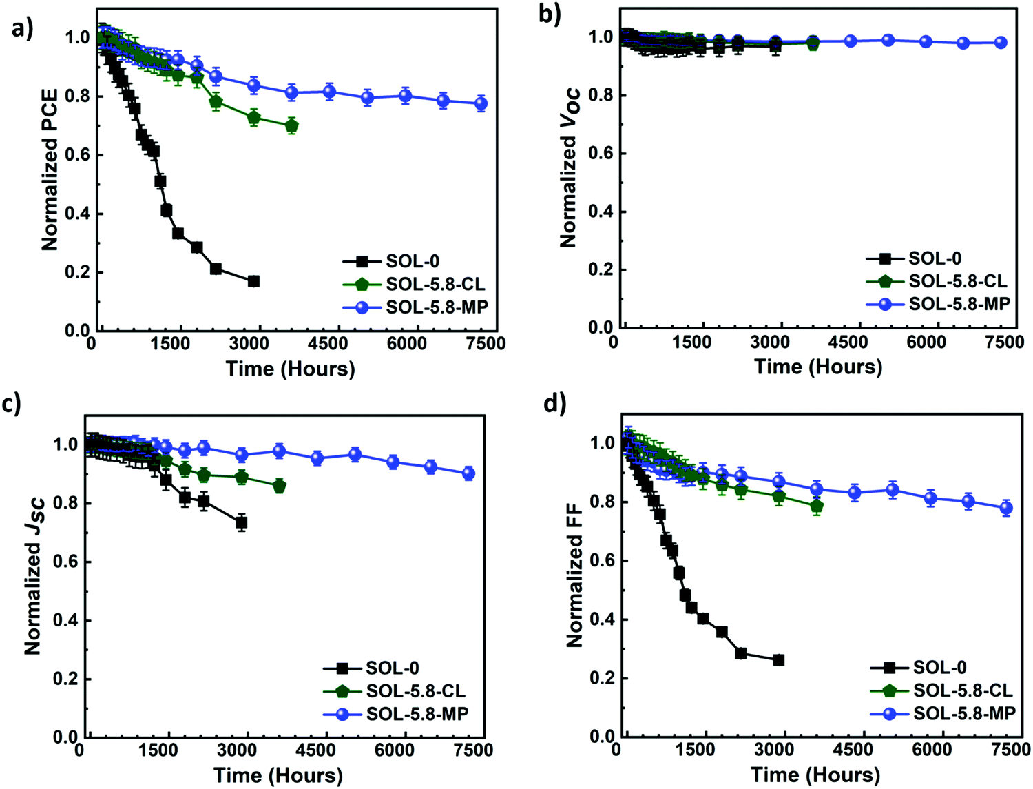 | ||
| Fig. 5 Evolution of J–V parameters (a) PCE, (b) Voc, (c) Jsc, and (d) FF for the different devices measured at different periods over ten months. Devices are always stored and measured under ambient laboratory conditions (T = 22–25 °C, and RH = 25–55% RH). | ||
As presented in Fig. 5(a), the SOL-0 solar cells degrade the fastest, with more than 50% of the PCE loss after the first 1200 hours. In contrast, SOL-5.8-based devices show remarkable stability with a 10% loss and only 6.6% loss in PCE for SOL-5.8-CL and SOL-5.8-MP, respectively. The most significant finding is that the SOL-5.8 solar cells are substantially more stable than the SOL-0-based solar cells as anticipated from the passivated grain boundaries. Indeed, the addition of SCN− improves the efficiency and stability of these perovskites by strong S–C–N intermolecular bonds in the perovskite lattice structure.31,32
We also obtained a long lifetime for the SOL-5.8-MP solar cells as determined by the T80 parameter (the time at which the device loses 20% of its initial PCE).55 Our solar cells exhibit a T80 of 523 hours for SOL-0-CL, 2091 hours for SOL-5.8-CL, and 5035 hours for SOL-5.8-MP, respectively. Notably, our recorded lifetime of >5000 hours is among the best-reported T80 so far for ambient condition-stable perovskite solar cells.55,56Fig. 5(b)–(d) display the degradation of the other J–V parameters. There, the devices show relatively constant Voc with minimal variation in all three devices. The Jsc and especially FF show substantial degradation. The FF degradation remains the dominant contributor to the PCE degradation in all the devices.
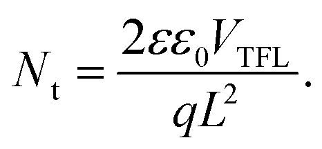
Seeking to unveil the device performance intricacies in terms of efficiency and stability, the trap-state densities and the charge transport57–59 mechanisms have been evaluated in both fresh and degraded single-carrier devices by the SCLC method.58,60 The hole-only (H-O) devices suppress the injection of electrons at the electrodes, while the electron-only (E-O) devices limit the injection of holes. Fig. 6(a)–(c) compare the log-scale J–V characteristics of the single-carrier devices, from which the trap density can be derived using the equation:61
 | (1) |
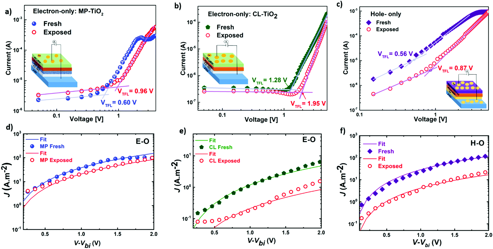 | ||
| Fig. 6 (a–c) Log-scale J–V curves in the dark indicating the trap-filled voltages (VTFL) and showing fitted curves (d–f) with the Mott–Gurney equation62 (SCLC method) for mobilities for fresh and exposed (240 hours under ambient conditions) electron-only devices (a and d) FTO/CL-MP-TiO2/SOL-5.8/PC71BM/Au device and (b and e) FTO/CL-TiO2/SOL-5.8/PC71BM/Au device; hole-only device (c and f) FTO/Au/SOL-5.8/spiro-OMeTAD/Au device. Insets: Electron-only device structures of (a) MP-TiO2, (b) CL-TiO2 and (c) hole-only device structure. | ||
The voltage at which the trap states are filled with charge carriers is known as the trap-filled limit voltage (VTFL). Nt is the trap density, q is the electronic charge, L is the thickness, ε is the dielectric constant of the material, and ε0 is the vacuum permittivity.
Fig. 6(a)–(c) display the log-scale J–V curves measured for the fresh and partially-degraded (after 240 hours or 10 days storage under ambient conditions) single-carrier devices with the corresponding VTFL. From the VTFL, the trap densities can be obtained using eqn (2)61 and are displayed in Table 2. In the fresh state, we observe a low trap-state density (down to 1015) in our perovskite thin films, which slightly increase after exposure to humidity (35% ± 5RH). This increment in Nt might contribute to the observed overall degradation over time.57 However, the real reason behind the observed degradation trends (MP-TiO2 ≫ CL-TiO2 ≫ SOL-0) remains unclear as the trap density increase does not readily correlate with the observed degradation and lifetime.
| Devices | Trap density fresh (×1016 cm−3) | Trap density exposed (×1016 cm−3) | Mobility (μ) fresh (×10−6 cm2 V−1 s−1) | Mobility (μ) exposed (×10−6 cm2 V−1 s−1) |
|---|---|---|---|---|
| The obtained mobility values of the fresh devices are comparable to those reported in the literature.63,64 | ||||
| E-O (with CL-Ti O2) | 1.50 | 2.29 | 6.25 | 1.10 |
| E-O (with MP-Ti O2) | 0.70 | 1.13 | 200 | 110 |
| H-O | 0.66 | 1.02 | 150 | 22 |
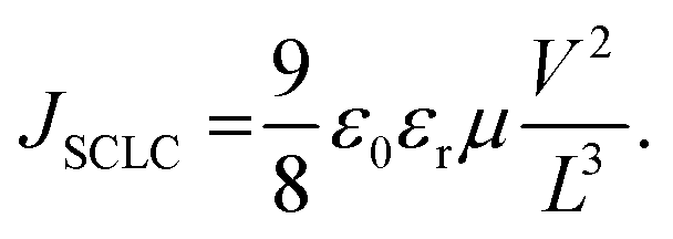
Any change in the charge transport (before and after exposure) may help explain the observed degradation trend. When the ratio of mobilities of electrons and holes is close to unity, there is a balanced charge transport. Imbalance in charge mobilities of electrons and holes before and after degradation has been suggested to be associated with the different carrier extraction rates and a reason behind the drop in FF.65–67 Therefore, to elucidate this issue further, we determined the charge carrier mobilities63,64 and the ratio of mobilities using the SCLC method as previously described.66 Though the SCLC method is simplistic, it has been used to determine carrier mobilities in the thin-film perovskite devices.63,64 The J–V curves of the fresh and exposed devices in Fig. 6(d)–(f) have been fitted to the Mott–Gurney equation62 to determine the charge carrier mobilities in the perovskite films.
 | (2) |
Table 2 suggests a high degree of imbalance in electron and hole mobilities in fresh CL-TiO2 cells (with a ratio of 24) compared to fresh MP-TiO2 cells (with a ratio of 1.3). The good balance in charge mobility of MP-TiO2 cells also explains the high FF of the MP-TiO2 cells, as seen in Table 1. It has been reported that unbalanced mobilities induce the build-up of space charge within the devices, reducing the charge extraction, and increasing the charge carrier densities.66 Bearing this in mind, even though there is an increase in this ratio for the degraded MP-TiO2 devices from 1.3 to 5, this is still a much smaller charge carrier imbalance than that of the fresh or degraded CL-TiO2 devices, which remains as high as 20. Hence, we conclude that imbalance in charge transport is a possible reason for the observed reduction in the FF, which is the strongest contribution to the PCE degradation, in turn, explaining the fact that the SOL-5.8-MP solar cells are significantly more stable than the SOL-5.8-CL cells.
Moreover, it is known that the FF is linked to the ratio of the extraction and recombination rates, and the mobilities of electrons and holes do affect both of them.68 Thus, the continuous drop in the FF (Fig. 5(d)) during the stability test narrows the origin of the degradation process down to a variation in recombination and/or extraction rates (evidenced by the drop in electron and hole currents seen in Fig. 6(d)–(f), but also by an increase in trap-state densities), to an imbalance in charge carrier mobilities.66 Therefore, the very low electron current measured for the CL-TiO2 devices (Fig. 6(e)) compared to that of the MP-TiO2 devices (Fig. 6(d)) could partly explain the observed degradation trend. Additionally, it is important to note that the better performance of the MP-TiO2 cells in terms of PCE is consistent with the lower trap-state density and charge balance compared to that of the CL-TiO2 devices. The detailed mechanisms behind the drop in mobilities (and the imbalance in charge transport) upon degradation are still unclear and beyond the scope of this work. Plans for further studies into the individual factors that may affect the performance of our solar cells are currently underway and would be based on the International Summit on Organic Photovoltaic Stability (ISOS) procedures. We believe that the ionic additive and solvent–anti solvent treatment play a crucial passivation role, resulting in the formation of pinhole-free and large grains, which helps to reduce the degradation rate of the perovskite material by preventing moisture penetration and accumulation. SCN− doping produces the stable pseudohalide perovskite due to enhanced chemical bonding in the lattice due to both strong ionic interactions between S–C–N and adjacent Pb and extra hydrogen bonding between SCN− and CH3NH3+.32 Additionally, the free energy difference ΔH for the decay being positive for the former and harmful for the latter, the SCN-doped perovskite does not spontaneously decay, unlike CH3NH3PbI3.32
Conclusion
In summary, a new reproducible method for ambient-condition fabrication of highly crystalline, compact, and large-grain halide perovskite films is presented. This new method is used for highly efficient and stable photovoltaic device integration. We have compared the perovskite solar cells undoped and doped with SCN using the perovskite precursors without (SOL-0) and with an optimal concentration of Pb(SCN)2 (SOL-5.8) atop both dense TiO2 (CL-TiO2) and mesoporous TiO2 on TiO2 (MP-TiO2) films as electron transport layers. The best performing device reaches a maximum power conversion efficiency of 20.3% under standard AM1.5G illumination with excellent reproducibility. Remarkably, the SOL-5.8-MP devices without any encapsulation show less than 20% PCE degradation after over 7000 hours (∼10 months) of exposure to ambient room conditions. The remarkable performance of these solar cells is mainly due to their superior structural quality with compact morphology, large grain size, reduced grain boundaries, and low-trap density, as well as to the better inherent stability of the pseudohalide perovskite. We also related the trap density and charge mobility in the perovskite devices to the reduced current density and fill factors of the devices stored under ambient room conditions. Our research work provides an important pathway towards the fabrication of ambient condition-processed, high efficiency, and stable perovskite solar cells using this precursor-based method.Experimental methods
The solvents and precursors were purchased from Ossila and Sigma Aldrich, unless otherwise stated, and used as received without any further modifications.Preparation of electron transport layers and perovskite films
Fluorine-doped tin oxide (FTO) (TEC 15, 12–14 Ω sq−1) glass substrates were used for the devices. The substrates were cleaned by ultrasonication with Hellmanex soap (10%) in water, deionized water, acetone, and isopropanol successively for 10 minutes and then dried with compressed air. The cleaned substrates were then treated with UV-ozone for 20 minutes preceding titanium dioxide (TiO2) deposition. Planar and mesoscopic solar cells with the following configuration FTO/CL-TiO2/perovskite/spiro-OMeTAD/Au and FTO/CL-TiO2/MP-TiO2/perovskite/spiro-OMeTAD/Au were fabricated. Each material was sequentially deposited via layer-by-layer spin-coating. First, a ∼50 nm compact TiO2 layer (Ti-nanoxide BL/SC, Solaronix SA) was spin-coated onto the cleaned FTO substrates, then annealed at 550 °C for 45 minutes in a quartz tube furnace and finally cooled down to room temperature. In the case of the second configuration, diluted (in ethanol 6![[thin space (1/6-em)]](https://www.rsc.org/images/entities/char_2009.gif) :1 volume ratio) mesoporous TiO2 (Great cell 30 NR-D) was spin-coated atop the compact TiO2 layer. The substrates were annealed at 500 °C for 30 min in air. After cooling the substrates to room temperature, lithium-doping of the mesoporous layer was carried out, following a modified method already described elsewhere.27 The mixed-cation–mixed halide perovskite of the form Csx(MA0.17FA0.83)Pb(100−x) (I0.83Br0.17)3 was modified by doping with lead thiocyanate to be resilient under ambient conditions and then used to prepare our solution (SOL-0). 2.9, 5.8, 9.4, and 11.1 wt% of SCN ions were added to the reference perovskite solution. To obtain the mixed-cation–mixed halide perovskite solution, we dissolved 0.6 M methylammonium iodide, 0.2 M methylammonium bromide, 1 M formamidinium iodide, 0.8 M lead(II) iodide and 0.5 M lead(II) bromide in mixed solvent DMSO/DMF at a 1:4 volume ratio. Then, a proportion of 1.5 M cesium iodide solution in DMSO was added to the perovskite solution and stirred gradually for one hour. No pre-heating of the solution was required before their deposition. The perovskite solution69 was then deposited onto the glass/FTO/TiO2 layer and spin-coated at 2000 rpm for 20 s to obtain the desired thickness. In a dynamic spin-coating mode, the solvent–antisolvent treatment (chlorobenzene:ethanol in voume ratios) was carried out and spun at 5000 rpm for 10 s. After spin coating, the films were then annealed at 125 °C for 15 minutes to complete the crystallization process of the perovskite and to evaporate the excess solvents. The fabrication steps took place under ambient conditions: 22–25 °C, and 25–55% RH.
:1 volume ratio) mesoporous TiO2 (Great cell 30 NR-D) was spin-coated atop the compact TiO2 layer. The substrates were annealed at 500 °C for 30 min in air. After cooling the substrates to room temperature, lithium-doping of the mesoporous layer was carried out, following a modified method already described elsewhere.27 The mixed-cation–mixed halide perovskite of the form Csx(MA0.17FA0.83)Pb(100−x) (I0.83Br0.17)3 was modified by doping with lead thiocyanate to be resilient under ambient conditions and then used to prepare our solution (SOL-0). 2.9, 5.8, 9.4, and 11.1 wt% of SCN ions were added to the reference perovskite solution. To obtain the mixed-cation–mixed halide perovskite solution, we dissolved 0.6 M methylammonium iodide, 0.2 M methylammonium bromide, 1 M formamidinium iodide, 0.8 M lead(II) iodide and 0.5 M lead(II) bromide in mixed solvent DMSO/DMF at a 1:4 volume ratio. Then, a proportion of 1.5 M cesium iodide solution in DMSO was added to the perovskite solution and stirred gradually for one hour. No pre-heating of the solution was required before their deposition. The perovskite solution69 was then deposited onto the glass/FTO/TiO2 layer and spin-coated at 2000 rpm for 20 s to obtain the desired thickness. In a dynamic spin-coating mode, the solvent–antisolvent treatment (chlorobenzene:ethanol in voume ratios) was carried out and spun at 5000 rpm for 10 s. After spin coating, the films were then annealed at 125 °C for 15 minutes to complete the crystallization process of the perovskite and to evaporate the excess solvents. The fabrication steps took place under ambient conditions: 22–25 °C, and 25–55% RH.
Device fabrication
The perovskite solutions were deposited on the substrates and processed by using the two-step spin coating method described above. The first step was the casting of the perovskite precursor solution onto the FTO/TiO2 layer, followed by solvent-antisolvent (a mixture of ethanol and chlorobenzene) dripping. The films were then annealed to complete the crystallization process of the perovskite and to evaporate the excess solvents. The hole-transporting material, spiro-OMeTAD, was subsequently deposited, also by spin-coating, atop the FTO/CL-TiO2/MP-TiO2/perovskite layer. The spiro-OMeTAD solution was prepared following a previously reported procedure.21 The spiro-OMeTAD solution was then spin-coated atop the perovskite at 3500 rpm for 30 seconds in ambient air. The devices were stored under ambient conditions for 24 hours prior to the contact deposition. Finally, the devices were completed by thermal evaporation of a 100 nm gold layer to serve as a top electrode, deposited at 0.2 nm s−1 at a pressure of 5 × 10⁻⁵ Torr. The active illuminated area for all the devices was 0.45 cm × 0.15 cm, as defined by the area of the mask.Single-carrier device fabrication
The single-carrier devices also were fabricated by the spin-coating method. The hole-only devices were fabricated by depositing a ∼60 nm gold layer on top of FTO via thermal evaporation, followed by spin-coating the perovskite precursor solution at 2000 rpm for 25 s; then the spiro-OMeTAD solution was spin-coated at 3000 rpm for 30 s and finally ∼80 nm of the gold layer as the top electrode was deposited via thermal evaporation. The electron-only devices were fabricated by spin-coating the perovskite solution on the FTO/TiO2 layer at 2000 rpm for 25 s, followed by spin-casting [6,6]-phenyl-C71-butyric acid methyl ester (PC71BM) solution (15 mg ml−1 in chlorobenzene) at 1500 rpm for 30 s, and finally, the gold electrode was thermally evaporated. Note that, after each step of depositing the perovskite layers, they were annealed, and cooled down to room temperature before spin-coating the following top layers. The active transport layer of the devices used for the stability measurement was also exposed to ambient conditions before the evaporation of the top electrodes.Materials and device characterization
The morphologies of the films were characterized by SEM, using a Hitachi SU 8230 ultra-high-resolution field emission scanning electron microscope. X-ray powder diffraction (XRD) patterns of the polycrystalline material were collected using a Bruker-AXS D8 Advance X-ray diffractometer with Cu Kα1 radiation (λ = 1.5406 Å). JEOL JAMP-30 was used for the Auger electron spectroscopy (AES) measurement. It was equipped with a LaB6 electron gun and was operated at 10 kV during the analysis. The Auger detector is a cylindrical mirror analyzer (CMA) and can detect Auger electrons from 0 to 3 keV. The acquisition system software was upgraded from the original to the one made by Geller MicroAnalytical Laboratory, Inc. (GMAL). The spectral measurements were done by placing the beam on the area of interest and collecting a 0–1000 eV spectrum, which takes about 1 minute. The electron beam current used was 5 × 10⁻⁷ Amp.The absorption spectra of the films were obtained using a UV/VIS/NIR spectrophotometer (PerkinElmer Lambda 750). The J–V characteristics were measured with a Keithley 2400 source meter under AM1.5G illumination at 100mW cm−2 using a Newport solar simulator (Newport, model 91160-1000). Finally, external quantum efficiency (EQE) measurements and integrated current density calculations were performed following the same procedure as the one reported previously.70 The photocurrent spectrum was measured using a xenon lamp coupled to a TRIAX320 monochromator equipped with a chopper and a lock-in amplifier (Ametek 1256) at zero bias. The light from the xenon lamp passes through the monochromator and was then modulated at 100 Hz before arriving on the solar cell placed behind a circular diaphragm of diameter 0.18 cm. The photocurrent, I(λ), was measured utilizing the lock-in amplifier. The EQE was calculated using the formula: 100 hcI(λ)/qλP(λ), where c is the speed of light, h is the Planck constant, and q is the electronic charge. The incident power, P(λ), was measured with a calibrated photodiode (Newport 918D) placed at the position of the sample with the same diaphragm aperture. The integrated current density (Jint) is calculated from the EQE data, using the equation:  , where F(λ) is the photon flux as a function of the wavelength in units of W cm−2 nm−1 under AM1.5G illumination and q is the electron charge. We used the photon flux values downloaded from the internet (http://rredc.nrel.gov/solar/spectra/am1.5/).
The power of the incident light was measured using a calibrated photodiode (Newport 918D). The hysteresis index (HI) was determined by using the modified relation:46
 | (3) |
Conflicts of interest
The authors declare no competing financial and/or non-financial interests in relation to this work. The authors also declare no conflict of interest.Acknowledgements
I. M. A. acknowledges the UNESCO Chairs of MATECSS for her PhD Excellence Scholarship. I. M. A. and I. K. are thankful to the FRQNT for their doctoral and postdoctoral fellowships, respectively. S. G. C., R. N., and A. P. are thankful to the NSERC Discovery Program. S. G. C. also thanks the Canada Research Chairs and the FRQNT-Team program for their financial support. N. Y. D. acknowledges the financial support from the Zernike Bonus Incentive Scheme. The authors would also like to acknowledge S. Basu for her help with some measurements.References
- https://www.nrel.gov/pv/assets/images/efficiency-chart-20180716.jpg .
- I. M. Asuo, D. Gedamu, I. Ka, L. F. Gerlein, F.-X. Fortier, A. Pignolet, S. G. Cloutier and R. Nechache, Nano Energy, 2018, 51, 324–332 CrossRef CAS.
- S. D. Stranks, G. E. Eperon, G. Grancini, C. Menelaou, M. J. P. Alcocer, T. Leijtens, L. M. Herz, A. Petrozza and H. J. Snaith, Science, 2013, 342, 341–344 CrossRef CAS PubMed.
- H. S. Jung and N.-G. Park, Small, 2015, 11, 10–25 CrossRef CAS PubMed.
- J. C. Yu, D. Bin Kim, E. D. Jung, B. R. Lee and M. H. Song, Nanoscale, 2016, 8, 7036–7042 RSC.
- B. R. Sutherland and E. H. Sargent, Nat. Photonics, 2016, 10, 295–302 CrossRef CAS.
- K. Young-Hoon, C. Himchan, H. J. Hyuck, K. Tae-Sik, M. NoSoung, L. Chang-Lyoul, I. S. Hyuk and L. Tae-Woo, Adv. Mater., 2014, 27, 1248–1254 Search PubMed.
- X. Li, D. Bi, C. Yi, J.-D. Décoppet, J. Luo, S. M. Zakeeruddin, A. Hagfeldt and M. Grätzel, Science, 2016, 353, 58–62 CrossRef CAS PubMed.
- J.-H. Im, I.-H. Jang, N. Pellet, M. Grätzel and N.-G. Park, Nat. Nanotechnol., 2014, 9, 927–932 CrossRef CAS PubMed.
- L. Kyung-Geun, K. Hak-Beom, J. Jaeki, K. Hobeom, K. J. Young and L. Tae-Woo, Adv. Mater., 2014, 26, 6461–6466 CrossRef PubMed.
- L. Shen, Y. Lin, C. Bao, Y. Bai, Y. Deng, M. Wang, T. Li, Y. Lu, A. Gruverman, W. Li and J. Huang, Mater. Horiz., 2017, 4, 242–248 RSC.
- G. E. Eperon, S. D. Stranks, C. Menelaou, M. B. Johnston, L. M. Herz and H. J. Snaith, Energy Environ. Sci., 2014, 7, 982–988 RSC.
- I. M. Asuo, P. Fourmont, I. Ka, D. Gedamu, S. Bouzidi, A. Pignolet, R. Nechache and S. G. Cloutier, Small, 2019, 15, 1804150 CrossRef PubMed.
- T. A. Berhe, W.-N. Su, C.-H. Chen, C.-J. Pan, J.-H. Cheng, H.-M. Chen, M.-C. Tsai, L.-Y. Chen, A. A. Dubale and B.-J. Hwang, Energy Environ. Sci., 2016, 9, 323–356 RSC.
- F. El-Mellouhi, E. T. Bentria, S. N. Rashkeev, S. Kais and F. H. Alharbi, Sci. Rep., 2016, 6, 30305 CrossRef CAS PubMed.
- Y.-Y. Zhang, S. Chen, P. Xu, H. Xiang, X.-G. Gong, A. Walsh and S.-H. Wei, Chin. Phys. Lett., 2018, 35, 036104 CrossRef.
- N. Arora, M. I. Dar, M. Abdi-Jalebi, F. Giordano, N. Pellet, G. Jacopin, R. H. Friend, S. M. Zakeeruddin and M. Grätzel, Nano Lett, 2016, 16(11), 7155–7162 CrossRef CAS PubMed.
- J. Troughton, K. Hooper and T. M. Watson, Nano Energy, 2017, 39, 60–68 CrossRef CAS.
- S. Trilok, Ö. Senol, S. Alexander, F. Robert, M. Sanjay and M. Tsutomu, Adv. Funct. Mater., 2018, 28, 1706287 CrossRef.
- Q. Tai, P. You, H. Sang, Z. Liu, C. Hu, H. L. W. Chan and F. Yan, Nat. Commun., 2016, 7, 11105 CrossRef CAS PubMed.
- J. Burschka, N. Pellet, S.-J. Moon, R. Humphry-Baker, P. Gao, M. K. Nazeeruddin and M. Grätzel, Nature, 2013, 499, 316–319 CrossRef CAS PubMed.
- W. Nie, H. Tsai, R. Asadpour, J.-C. Blancon, A. J. Neukirch, G. Gupta, J. J. Crochet, M. Chhowalla, S. Tretiak, M. A. Alam, H.-L. Wang and A. D. Mohite, Science, 2015, 347, 522–525 CrossRef CAS PubMed.
- T. Niu, J. Lu, R. Munir, J. Li, D. Barrit, X. Zhang, H. Hu, Z. Yang, A. Amassian, K. Zhao and S. Liu, Adv. Mater., 2018, 30, 1706576, DOI:10.1002/adma.201706576.
- B. Wang, K. Y. Wong, S. Yang and T. Chen, J. Mater. Chem. A, 2016, 4, 3806–3812 RSC.
- D. Liu and T. L. Kelly, Nat. Photonics, 2014, 8, 133–138 CrossRef CAS.
- Y. Yu, C. Wang, C. R. Grice, N. Shrestha, D. Zhao, W. Liao, L. Guan, R. A. Awni, W. Meng, A. J. Cimaroli, K. Zhu, R. J. Ellingson and Y. Yan, ACS Energy Lett., 2017, 2, 1177–1182 CrossRef CAS.
- M. Saliba, T. Matsui, J.-Y. Seo, K. Domanski, J.-P. Correa-Baena, M. K. Nazeeruddin, S. M. Zakeeruddin, W. Tress, A. Abate, A. Hagfeldt and M. Grätzel, Energy Environ. Sci., 2016, 9, 1989–1997 RSC.
- N. Arora, M. I. Dar, A. Hinderhofer, N. Pellet, F. Schreiber, S. M. Zakeeruddin and M. Grätzel, Science, 2017, 358, 768–771 CrossRef CAS PubMed.
- J. M. Kadro, N. Pellet, F. Giordano, A. Ulianov, O. Mü, J. Maier, M. Grä and A. Hagfeldt, Energy Environ. Sci., 2016, 10, 3172–3179 RSC.
- D. Gedamu, I. M. Asuo, D. Benetti, M. Basti, I. Ka, S. G. Cloutier, F. Rosei and R. Nechache, Sci. Rep., 2018, 8, 12885 CrossRef PubMed.
- Q. Jiang, D. Rebollar, J. Gong, E. L. Piacentino, C. Zheng and T. Xu, Angew. Chem., Int. Ed., 2015, 54, 7617–7620 CrossRef CAS PubMed.
- A. M. Ganose, C. N. Savory and D. O. Scanlon, J. Phys. Chem. Lett., 2015, 6, 4594–4598 CrossRef CAS PubMed.
- W. Ke, C. Xiao, C. Wang, B. Saparov, H.-S. S. Duan, D. Zhao, Z. Xiao, P. Schulz, S. P. Harvey, W. Liao, W. Meng, Y. Yu, A. J. Cimaroli, C.-S. S. Jiang, K. Zhu, M. Al-Jassim, G. Fang, D. B. Mitzi and Y. Yan, Adv. Mater., 2016, 28, 5214–5221, DOI:10.1002/adma.201600594.
- A. Halder, R. Chulliyil, A. S. Subbiah, T. Khan, S. Chattoraj, A. Chowdhury and S. K. Sarkar, J. Phys. Chem. Lett., 2015, 6, 3483–3489 CrossRef CAS PubMed.
- X. Zhang, H. Liu, W. Wang, J. Zhang, B. Xu, K. L. Karen, Y. Zheng, S. Liu, S. Chen, K. Wang and X. W. Sun, Adv. Mater., 2017, 29, 1606405, DOI:10.1002/adma.201606405.
- J. Chen, J. Xu, S. Zhang, S. Zhou, K. Zhou, B. Zhang, X. Xia, Y. Liu, S. Dai and J. Yao, J. Phys. Chem. C, 2017, 7, 44 Search PubMed.
- Y.-H. Chiang, M.-H. Li, H.-M. Cheng, P.-S. Shen and P. Chen, ACS Appl. Mater. Interfaces, 2017, 9, 2403–2409 CrossRef CAS PubMed.
- Y. Chen, B. Li, W. Huang, D. Gao and Z. Liang, Chem. Commun., 2015, 51, 11997–11999 RSC.
- W. Ke, C. Xiao, C. Wang, B. Saparov, H.-S. Duan, D. Zhao, Z. Xiao, P. Schulz, S. P. Harvey, W. Liao, W. Meng, Y. Yu, A. J. Cimaroli, C.-S. Jiang, K. Zhu, M. Al-Jassim, G. Fang, D. B. Mitzi and Y. Yan, Adv. Mater., 2016, 28, 5214–5221 CrossRef CAS PubMed.
- M. K. Kim, T. Jeon, H. Il Park, J. M. Lee, S. A. Nam and S. O. Kim, CrystEngComm, 2016, 18, 6090–6095 RSC.
- Y. Zhou, O. S. Game, S. Pang and N. P. Padture, J. Phys. Chem. Lett., 2015, 6, 4827–4839 CrossRef CAS PubMed.
- T. S. Sherkar, C. Momblona, L. Gil-Escrig, J. Ávila, M. Sessolo, H. J. Bolink and L. J. A. Koster, ACS Energy Lett., 2017, 2(5), 1214–1222, DOI:10.1021/acsenergylett.7b00236.
- N. Liu, Q. Du, G. Yin, P. Liu, L. Li, H. Xie, C. Zhu, Y. Li, H. Zhou, W.-B. Zhang and Q. Chen, J. Mater. Chem. A, 2018, 6, 6806–6814 RSC.
- T. J. Jacobsson, J. P. Correa-Baena, E. Halvani Anaraki, B. Philippe, S. D. Stranks, M. E. F. Bouduban, W. Tress, K. Schenk, J. Teuscher, J. E. Moser, H. Rensmo and A. Hagfeldt, J. Am. Chem. Soc., 2016, 138, 10331–10343 CrossRef CAS PubMed.
- P. Scherrer, Nachrichten von der Gesellschaft der Wissenschaften zu Göttingen, Math. Klasse, 1918, pp. 98–100 Search PubMed.
- H.-S. Kim and N.-G. Park, J. Phys. Chem. Lett., 2014, 5, 2927–2934 CrossRef CAS PubMed.
- C. Lan, J. Luo, H. Lan, B. Fan, H. Peng, J. Zhao, H. Sun, Z. Zheng, G. Liang and P. Fan, Materials, 2018, 11(3), 355, DOI:10.3390/ma11030355.
- F. Giordano, A. Abate, J. P. Correa Baena, M. Saliba, T. Matsui, S. H. Im, S. M. Zakeeruddin, M. K. Nazeeruddin, A. Hagfeldt and M. Graetzel, Nat. Commun., 2016, 7, 10379 CrossRef CAS PubMed.
- E. Zimmermann, P. Ehrenreich, T. Pfadler, J. A. Dorman, J. Weickert and L. Schmidt-Mende, Nat. Photonics, 2014, 8, 669–672 CrossRef CAS.
- A. Nakane, H. Tampo, M. Tamakoshi, S. Fujimoto, K. M. Kim, S. Kim, H. Shibata, S. Niki and H. Fujiwara, J. Appl. Phys., 2016, 120, 064505 CrossRef.
- G.-J. A. H. Wetzelaer, M. Scheepers, A. M. Sempere, C. Momblona, J. Ávila and H. J. Bolink, Adv. Mater., 2015, 27, 1837–1841 CrossRef CAS PubMed.
- D. Bi, W. Tress, M. I. Dar, P. Gao, J. Luo, C. Renevier, K. Schenk, A. Abate, F. Giordano, J.-P. Correa Baena, J.-D. Decoppet, S. M. Zakeeruddin, M. K. Nazeeruddin, M. Grätzel and A. Hagfeldt, Sci. Adv., 2016, 2, e1501170 CrossRef PubMed.
- Z. Chu, M. Yang, P. Schulz, D. Wu, X. Ma, E. Seifert, L. Sun, X. Li, K. Zhu and K. Lai, Nat. Commun., 2017, 8, 2230 CrossRef PubMed.
- Y. Rong, Y. Hu, S. Ravishankar, H. Liu, X. Hou, Y. Sheng, A. Mei, Q. Wang, D. Li, M. Xu, J. Bisquert and H. Han, Energy Environ. Sci., 2017, 10, 2383–2391 RSC.
- L. K. Ono, Y. Qi and S. Frank Liu, Joule, 2018, 2, 1961–1990 CrossRef CAS.
- Z. Wang, D. P. McMeekin, N. Sakai, S. van Reenen, K. Wojciechowski, J. B. Patel, M. B. Johnston and H. J. Snaith, Adv. Mater., 2017, 29, 1604186 CrossRef PubMed.
- X. Du, T. Heumueller, W. Gruber, A. Classen, T. Unruh, N. Li and C. J. Brabec, Joule, 2018, 1–12 Search PubMed.
- N. Y. Doumon, G. Wang, R. C. Chiechi and L. J. A. Koster, J. Mater. Chem. C, 2017, 5, 6611–6619 RSC.
- J. A. Röhr, X. Shi, S. A. Haque, T. Kirchartz and J. Nelson, Phys. Rev. Appl., 2018, 9, 044017 CrossRef.
- R. H. Bube, J. Appl. Phys., 1962, 33, 1733–1737 CrossRef CAS.
- K. Poorkazem and T. L. Kelly, Sustainable Energy Fuels, 2018, 2, 1332–1341 RSC.
- P. N. Murgatroyd, J. Phys. D: Appl. Phys., 1970, 3, 308 Search PubMed.
- C. Chiang and C. Wu, Nat. Photonics, 2016, 10, 196–200 CrossRef CAS.
- W. Zhou, P. Zhou, X. Lei, Z. Fang, M. Zhang, Q. Liu, T. Chen, H. Zeng, L. Ding, J. Zhu, S. Dai and S. Yang, ACS Appl. Mater. Interfaces, 2018, 10(2), 1897–1908, DOI:10.1021/acsami.7b15008.
- N. Y. Doumon, M. V. Dryzhov, F. V. Houard, V. M. Le Corre, A. Rahimi Chatri, P. Christodoulis and L. J. A. Koster, ACS Appl. Mater. Interfaces, 2019, 11, 8310–8318 CrossRef CAS PubMed.
- N. Y. Doumon, F. V. Houard, J. Dong, H. Yao, G. Portale, J. Hou and L. J. A. Koster, Org. Electron., 2019, 69, 255–262 CrossRef CAS.
- N. Y. Doumon, F. V. Houard, J. Dong, P. Christodoulis, M. V. Dryzhov, G. Portale and L. J. A. Koster, J. Mater. Chem. C, 2019, 7, 5104–5111 RSC.
- D. Bartesaghi, I. D. C. Pérez, J. Kniepert, S. Roland, M. Turbiez, D. Neher and L. J. A. Koster, Nat. Commun., 2015, 6, 7083 CrossRef CAS PubMed.
- Perovskite Inks|Pi-SOL Technologies Inc.|Canada, https://www.pisoltechnologies.com/, accessed 25 June 2019.
- I. Ka, I. M. Asuo, S. Basu, P. Fourmont, D. M. Gedamu, A. Pignolet, S. G. Cloutier and R. Nechache, Small, 2018, 14, 1802319 CrossRef PubMed.
Footnote |
| † Electronic supplementary information (ESI) available. See DOI: 10.1039/d0ma00528b |
| This journal is © The Royal Society of Chemistry 2020 |