
 Open Access Article
 This Open Access Article is licensed under a
 Creative Commons Attribution 3.0 Unported Licence
Comparison of fluorene, silafluorene and carbazole as linkers in perylene monoimide based non-fullerene acceptors†
Stefan
Weber
 a,
Jakob
Hofinger
b,
Thomas
Rath
a,
Matiss
Reinfelds
a,
David
Pfeifer
c,
Sergey M.
Borisov
c,
Peter
Fürk
a,
Heinz
Amenitsch
d,
Markus C.
Scharber
b and
Gregor
Trimmel
*a
a,
Jakob
Hofinger
b,
Thomas
Rath
a,
Matiss
Reinfelds
a,
David
Pfeifer
c,
Sergey M.
Borisov
c,
Peter
Fürk
a,
Heinz
Amenitsch
d,
Markus C.
Scharber
b and
Gregor
Trimmel
*a
aInstitute for Chemistry and Technology of Materials (ICTM), NAWI Graz, Graz University of Technology, Stremayrgasse 9, 8010 Graz, Austria. E-mail: gregor.trimmel@tugraz.at
bLinz Institute for Organic Solar Cells (LIOS), Institute of Physical Chemistry, Johannes Kepler University Linz, Altenbergerstrasse 69, 4040 Linz, Austria
cInstitute of Analytical Chemistry and Food Chemistry, NAWI Graz, Graz University of Technology, Stremayrgasse 9, 8010 Graz, Austria
dInstitute of Inorganic Chemistry, NAWI Graz, Graz University of Technology, Stremayrgasse 9, 8010 Graz, Austria
First published on 3rd September 2020
Abstract
Perylene monoimide (PMI) based non-fullerene acceptors are an interesting alternative to perylene diimide acceptors in organic photovoltaics due to an open substitution side allowing chemical modifications of the molecule. In addition, this offers the possibility to twist the molecule to avoid pronounced π–π stacking. At the same time, the good solubility and the well-suited optical properties are maintained. This work provides a new perspective of perylenes using PMI-linker-PMI based acceptors in which the linker is composed of different fluorene derivatives to investigate the influence of heteroatoms on the optical and electronic properties. The three compounds PMI-F-PMI, PMI-FSi-PMI and PMI-FN-PMI were synthesized using a fluorene (F), silafluorene (FSi) and carbazole (FN) linker, respectively, characterized regarding optical, structural and electronic properties and implemented in solar cells using PBDB-T as donor material. The influence of the donor/acceptor ratio as well as thermal annealing on the solar cell properties were studied and maximum device efficiencies of 5.16% and high photovoltages up to 1.14 V were obtained for all three acceptors. Moreover, the solar cells display reasonable stability in inert conditions as is exemplified by maximum power point tracking experiments under continuous illumination.
Introduction
Bulk heterojunction organic solar cells offer various advantages over conventional photovoltaic technologies such as light weight, flexibility and easy continuous roll-to-roll processability.1,2 This opens up a broad range of possible commercial applications in the future in the areas of building integrated photovoltaics, mobility, consumer goods and more. Within the era of polymer/fullerene solar cells, a large part of the research was focused on the design of various donor materials to optimize the power output leading to maximum device efficiencies of around 10%.3,4 However, fullerene derivatives suffer from low absorption in the visible range, aggregation in blend films and high production costs and thus ushered a new era of materials, the so called non-fullerene acceptors (NFAs) or small molecule acceptors (SMAs).2,5–7 This new material class offers several advantages such as tunable HOMO/LUMO levels and spectral adjustments by molecular design as well as higher stability in many cases.8–12 Implemented in bulk heterojunction solar cells, device efficiencies of 16% were already reached with various donor/acceptor material combinations using the SMAs BTP-4X13 and Y6.14–16 Recently, PCE values of 17.35% have been reported.17Among the broad variety of different structures, NFAs based on perylenes have been in the focus since the beginning of organic solar cell research and were used in the first organic heterojunction solar cell by C. W. Tang back in 1986.18 So far, mainly perylene diimides (PDI), substituted at the bay position were investigated as NFAs in solar cells.19–25 The major issue of PDIs is their pronounced agglomeration, which leads to large crystallites within the blend and hence low device performance.26–28 To tackle this issue, twisting the PDI is necessary by introducing side groups or by ring fusion.29,30 Following these strategies, recently maximum device efficiencies of 10% were reached with PDI based acceptors.29,31,32
A very interesting approach is to link two perylene monoimides (PMI) by a conjugated linker, to form a perylene-linker-perylene triad structure (compare Scheme 1, e.g. using alkinyl, thiophene or fluorene linkers).33–38 In the case of electron rich linkers, this results in an acceptor–donor–acceptor structure, a structure realized in most of the high efficient NFAs such as Y6 or BTP-4X. Recently, Zhang et al. demonstrated that a simple fluorene linker, combined with perylene monoimide electron withdrawing groups, reaches in combination with PTZ1 PCEs up to 6%.37,38
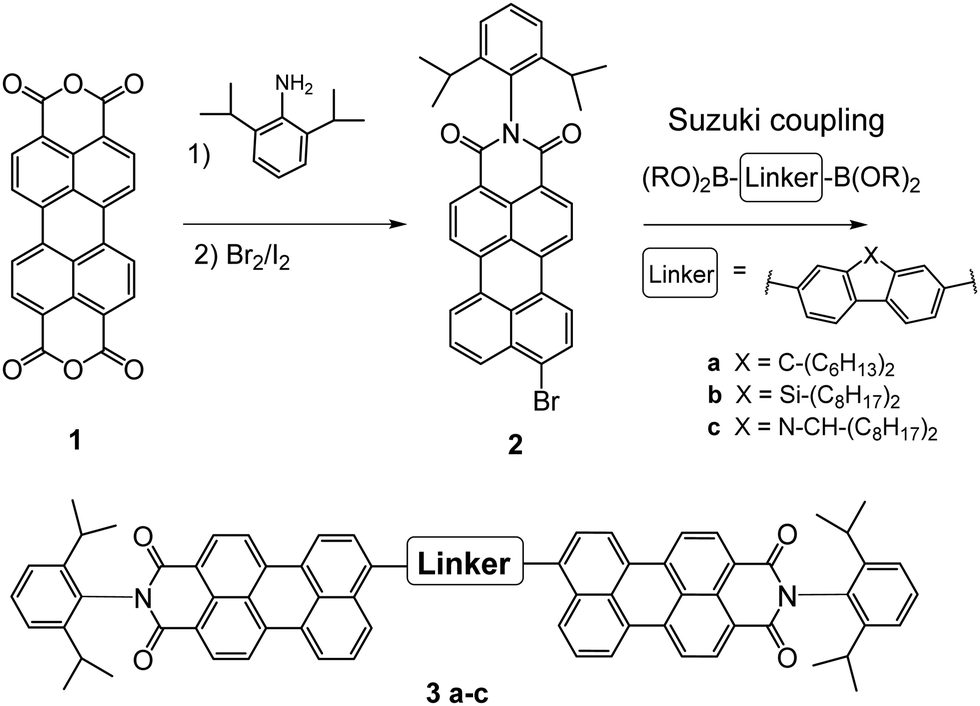 | ||
| Scheme 1 Synthesis of perylene-linker-perylene NFAs 3a–c. | ||
Although the efficiencies are moderate, extremely high open circuit voltages of 1.32 V were reached due to the high lying LUMO level of PMI-F-PMI.38
These high VOC values inspired us to investigate this type of NFAs in more detail. Therefore, this study compares a PMI-fluorene-PMI-acceptor molecule with its carbazole and silafluorene analogues in order to investigate the influence of the heteroatom in the fluorene-based core. Their optical, structural and electronic properties were thoroughly characterized and additionally supported by density functional theory (DFT) calculations. Moreover, all three compounds were evaluated in bulk heterojunction solar cells using PBDB-T as donor polymer in an inverted device setup.
Results and discussion
The PMI-aryl-PMI NFAs were synthesized as outlined in Scheme 1. The key step for the synthesis of these compounds was a Suzuki coupling reaction, using commercially available diboronic acid esters of the corresponding linker molecules and perylene monoimide bromide to give in the case of the fluorene linker the compound PMI-F-PMI (3a), of the silafluorene linker PMI-FSi-PMI (3b) and of the carbazole linker PMI-FN-PMI (3c). Pd(PPh3)4 and aqueous K2CO3 in refluxing toluene were used as standard coupling conditions. A detailed synthesis procedure is given in the ESI.†The structures were verified by 1H- and 13C-NMR spectroscopy and MALDI-TOF mass spectrometry and are shown in the ESI.† Owing to the long alkyl side chains, all three synthesized compounds exhibited good solubility in common organic solvents such as dichloromethane, chloroform, chlorobenzene (CB) or dichlorobenzene. Furthermore, all compounds demonstrated excellent thermal stability. The decomposition temperatures (TGA, see Fig. S10, ESI†) of PMI-F-PMI, PMI-FSi-PMI and PMI-FN-PMI are 441 °C, 471 °C and 465 °C, respectively. The minor mass loss of up to 3% in the PMI-FSi-PMI sample below 400 °C can be assigned to low amounts of residual solvent in the sample.
Computations
Density functional theory (DFT) computations were conducted in order to analyze the influence of the heteroatom on the structure as well as on the optical and electrical properties. The ground state geometries were optimized and the obtained minima were verified by frequencies calculations (B3LYP/6-31G*/Gaussian 09).39 A representation of the results is shown for all three compounds 3a–c in Fig. S11 (ESI†). In all three cases a twist between the fluorene-type linker and the PMI units is observed with a similar dihedral angle of approximately 55° between the PMI and linker moieties. The frontier molecular orbitals of all three compounds are essentially isolobal. In the HOMO, the electron density is distributed alongside the perylene backbone and fluorene, whereas in the LUMO the electron density is shifted towards the perylene backbone (Fig. 1). The nodal plane passes through the imide in the HOMO and LUMO orbitals, thus the imide substitution should not influence spectral and electrochemical properties of the molecule. However, due to the bulky isopropyl groups, the phenyl substituent on the imide moiety is oriented perpendicularly to the rest of the molecule. This as well as the aliphatic side chain on the central linker moiety suppress the aggregation of the molecule and increases the solubility. The HOMO and LUMO energy levels of PMI-F-PMI (3a) are predicted to be −5.42 and −2.88 eV, respectively (bandgap 2.54 eV). The silafluorene (3b) and carbazole (3c) based NFAs have values nearly identical to PMI-F-PMI (see Table 1).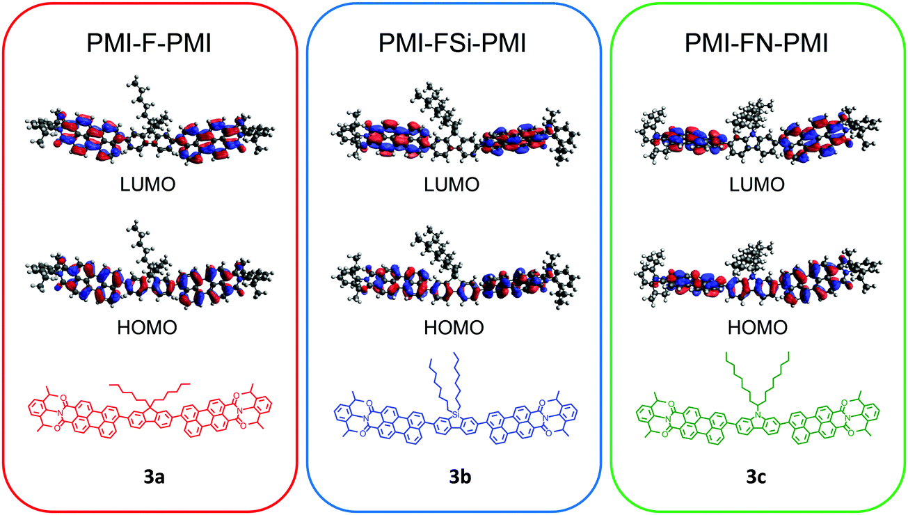 | ||
| Fig. 1 DFT (B3LYP/6-31G*) – molecular geometries and the frontier molecular orbitals of PMI-F-PMI (3a), PMI-FSi-PMI (3b) and PMI-FN-PMI (3c). | ||
| Material | HOMODFT (eV) | LUMODFT (eV) | E DFTg (eV) |
|---|---|---|---|
| PMI-F-PMI | −5.42 | −2.88 | 2.54 |
| PMI-FSi-PMI | −5.44 | −2.88 | 2.56 |
| PMI-FN-PMI | −5.40 | −2.86 | 2.54 |
Optical and electronic properties
UV-Vis absorption spectra of the synthesized NFAs (PMI-F-PMI, PMI-FSi-PMI and PMI-FN-PMI) were compared to those of the monomeric PMI compounds PMI-Br (2) as well as PMI-H (without bromide) in chloroform solution and are depicted in Fig. 2A. In solution, PMI-H and PMI-Br (2) exhibit two absorption peaks whereas all three acceptors 3a–c have less resolved absorption peaks. Due to the increased π-system of the linked molecules, the absorption spectra are 19 nm redshifted compared to PMI-Br (Table 2). This was also reported by Y. Zhang et al. for PMI-F-PMI.37 Absorption spectra of thin films on glass substrates of PMI-F-PMI, PMI-FSi-PMI, PMI-FN-PMI (see Fig. 2B) are broadened compared to their spectra in solution which is due to π–π stacking. | ||
| Fig. 2 (A) Optical absorption spectra of PMI, PMI-Br (2), PMI-F-PMI (3a), PMI-FSi-PMI (3b) and PMI-FN-PMI (3c) in solution (chloroform); (B) thin film absorption spectra of PMI-F-PMI (3a), PMI-FSi-PMI (3b), PMI-FN-PMI (3c) and PBDB-T. | ||
| Material | λ max,sol. (nm) | λ onset (sol.) (nm) | λ max,(fluor.,sol.) (nm) | ϕ FL | E g (eV) | ε (M−1 cm−1) | λ max,film (nm) | HOMOc (eV) | LUMOc (eV) | μ e_FET (saturation) (cm2 V−1 s−1) | μ e_FET (linear) (cm2 V−1 s−1) |
|---|---|---|---|---|---|---|---|---|---|---|---|
| a Solution. b Thin film. c Determined by CV. | |||||||||||
| PMI | 485 | 539 | 539 | 0.81 | 2.30a | 3.3 × 10⁴ | — | — | — | — | — |
| PMI-Br | 511 | 541 | 541 | 0.86 | 2.29a | 3.3 × 10⁴ | — | — | — | — | — |
| PMI-F-PMI | 530 | 575 | 587 | 0.74 | 2.16a/2.06b | 9.0 × 10⁴ | 516 | −6.12 | −3.93 | 2.4 × 10⁻⁴ | 1.9 × 10⁻⁴ |
| PMI-FSi-PMI | 530 | 573 | 585 | 0.74 | 2.16a/2.06b | 8.9 × 10⁴ | 523 | −6.12 | −3.97 | 1.3 × 10⁻⁴ | 1.1 × 10⁻⁴ |
| PMI-FN-PMI | 530 | 576 | 595 | 0.72 | 2.16a/2.06b | 8.8 × 10⁴ | 536 | −6.16 | −3.94 | 1.6 × 10⁻⁴ | 1.2 × 10⁻⁴ |
The molar absorption coefficients (in solution) for all compounds were calculated. Herein, the linked molecules, containing two PMI units, show almost three times higher values of the absorption coefficient (8.9–9.0 × 10⁴ M−1 cm−1) compared to the starting materials (3.3 × 10⁴ M−1 cm−1). This can be ascribed to the extended π-system within the molecules 3a–c.
All compounds show fluorescence in solution (chloroform) with a Stokes shift of 57 nm, 55 nm and 65 nm and nearly identical fluorescence quantum yields to be 0.74, 0.74 and 0.72 for PMI-F-PMI, PMI-FSI-PMI and PMI-FN-PMI, respectively (Fig. S12, ESI† and Table 2). These values are only slightly lower than those of the PMI-H and PMI-Br (0.81 and 0.86 respectively), indicating that the introduction of the linker with long alkyl side chains does not result in a large increase of (unfavorable) non-radiative relaxation pathways from the excited state.
Furthermore, fluorescence excitation and emission scans of the acceptor thin films were performed under ambient conditions (Fig. 3). The optical band gap energies were determined from the intersection between the excitation and emission spectra, since this method is less sensitive to scattering effects compared to the commonly used method of determining the optical band gap from the onset of the absorption spectrum.40 The small inset in Fig. 3 depicts an enlarged view of the intersection region around 600 nm and shows that the excitation and emission spectra intersect at 601, 602 and 601 nm for PMI-F-PMI, PMI-FSi-PMI and PMI-FN-PMI, respectively. This translates to an optical band gap of 2.06 eV for all three materials (Table 2).
 | ||
| Fig. 3 Normalized fluorescence excitation (solid lines) and emission (dashed lines) spectra of the PMI-X-PMI compounds in CHCl3 solution. | ||
In addition to the optical bandgap, the electrochemical bandgap was investigated performing cyclic voltammetry (CV) measurements on drop-casted films of PMI-F-PMI, PMI-FSi-PMI and PMI-FN-PMI, as well as of the donor polymer PBDB-T. The oxidation and reduction onsets were determined from CV measurements as shown in Fig. S13 (ESI†). HOMO and LUMO energy levels of the investigated materials were calculated according to the equations described in the experimental section and the results are depicted in Table 2. The electrochemical measurements suggest only minor differences between the respective HOMO and LUMO levels of the newly synthesized acceptor materials, which is supported by almost identical optical properties observed in absorbance and fluorescence measurements. Electrochemical bandgaps of 2.19, 2.15 and 2.22 eV were obtained for PMI-F-PMI, PMI-FSi-PMI and PMI-FN-PMI respectively, which are in good agreement with the reported electrochemical bandgap of PMI-F-PMI in literature.38
For the investigation of the performance of PMI-F-PMI, PMI-FSi-PMI and PMI-FN-PMI in solar cells, PBDB-T was selected as donor material due to its optoelectronic properties, which fit well to the three synthesized NFAs, as well as due to its good solubility and processability.4 The chemical structure of PBDB-T is shown in Scheme 2. A HOMO level of −5.89 eV and a LUMO level of −3.45 eV were determined from CV measurements of PBDB-T. These values result in a HOMO energy level offset of approximately 0.25 eV and a LUMO level offset of around 0.5 eV compared to the energy levels of PMI-F-PMI, PMI-FSi-PMI and PMI-FN-PMI.
 | ||
| Scheme 2 Structure of the conjugated polymer PBDB-T. | ||
In order to investigate the electronic properties of the newly synthesized acceptor materials, organic field effect transistors were fabricated with PMI-F-PMI, PMI-FSi-PMI and PMI-FN-PMI in a bottom-gate, top-contact geometry as shown in Fig. S14 (ESI†). The electron mobilities in the linear and saturation regime were extracted from OFET transfer characteristic measurements. The measurements are shown in Fig. S15 (ESI†) and the determined electron mobilities are presented in Table 2. All three acceptors exhibit similar values of OFET electron mobility in the range of low 10−4 cm2 V−1 s−1.
Crystallization properties and molecular packing
In a next step, we performed grazing incidence wide angle X-ray scattering (GIWAXS) measurements to study the crystallinity and molecular packing of the synthesized compounds. Fig. 4 shows the 2D-GIWAXS patterns of pristine PMI-F-PMI, PMI-FSi-PMI and PMI-FN-PMI thin films. In the GIWAXS images of the samples without annealing as well as in the corresponding line cuts in in-plane and out-of-plane direction (Fig. 4A–D) only weak features are visible. After annealing of the films at 150 °C, the crystallinity and order of the molecules is enhanced and more distinct signals are revealed (see Fig. 4E–H), which are most pronounced for PMI-FSi-PMI. This sample shows diffraction peaks at 2.6 and 4.1 nm−1 in the in-plane direction, which correlates to distances of 2.4 and 1.5 nm and suggests a two-dimensional order. Moreover, these peaks in the in-plane direction are characteristic for a preferential face-on orientation with respect to the substrate. The signal at 17.9 nm−1 in out-of-plane direction corresponds to a d-spacing of 0.35 nm, which indicates π–π stacking. Due to the fact that also for the PMI-F-PMI and PMI-FN-PMI films a broad diffraction peak around 4 nm−1 in in-plane direction is observed, we also assume a preferential, disordered face-on orientation in these samples. However, no pronounced crystallization of the investigated NFAs is suggested by the GIWAXS data.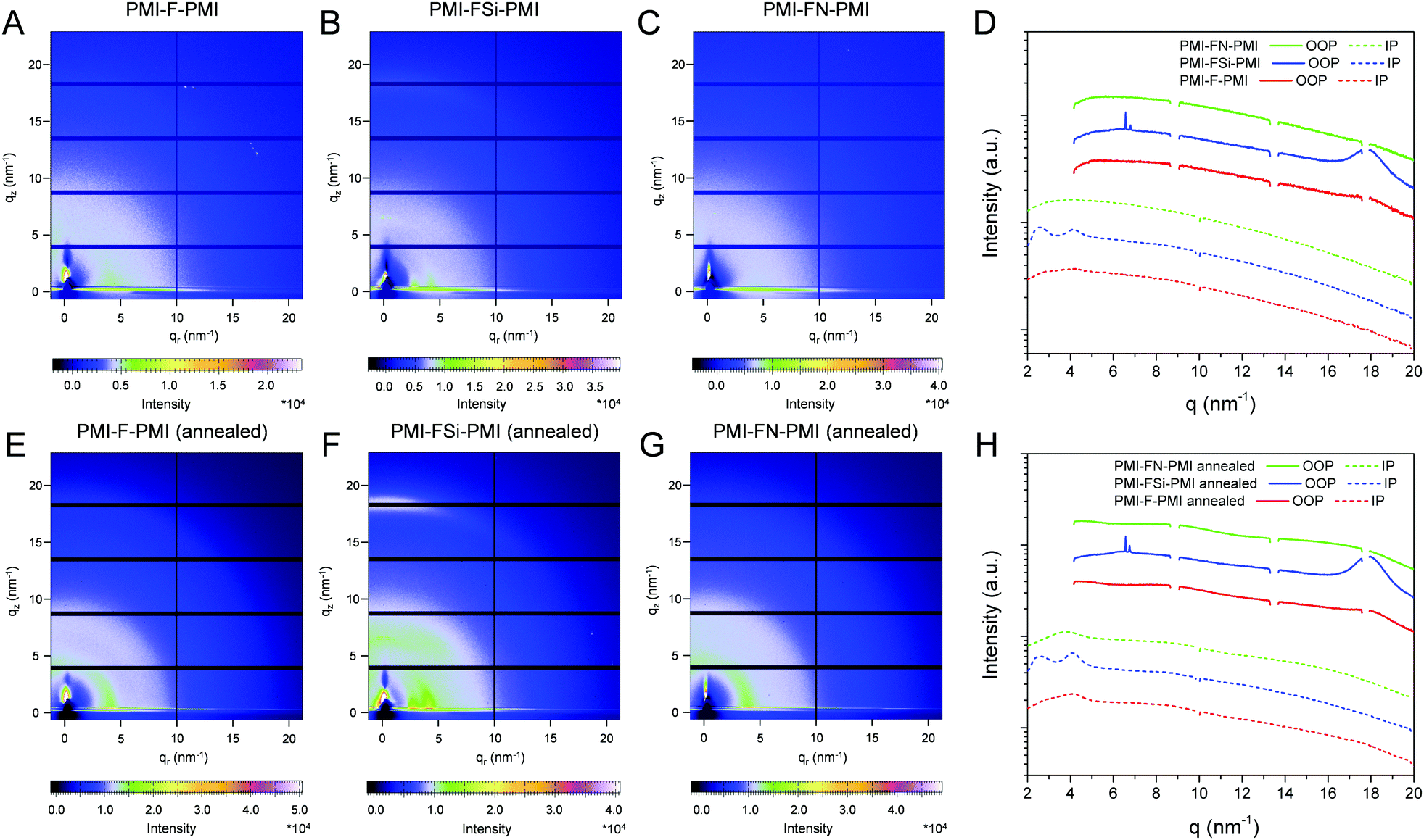 | ||
| Fig. 4 2D GIWAXS patterns of: (A) PMI-F-PMI (3a), (B) PMI-FSi-PMI (3b) and (C) PMI-FN-PMI (3c) w/o annealing and (E) PMI-F-PMI (3a), (F) PMI-FSi-PMI (3b) and (G) PMI-FN-PMI (3c) w. annealing. (D and H) The corresponding 1D line cuts in in-plane (IP) and out-of-plane (OOP) direction. The scattering profiles are shifted vertically for better visibility. | ||
The GIWAXS images of pristine PBDB-T films without and with annealing are depicted in Fig. S16 (ESI†). According to previous reports in the literature,41,42 the GIWAXS images reveal a typical pattern for preferential face-on orientation. The most pronounced features are a diffraction peak in the out-of-plane direction at 17.0 nm−1, corresponding to a π–π stacking distance of 0.37 nm and a lamellar diffraction peak at 2.85 nm−1 in in-plane direction corresponding to a lamellar d-spacing of 2.2 nm.
In the blend films of PBDB-T and the investigated NFAs (Fig. 5), the signals stemming from the individual components are combined in the GIWAXS patterns, which indicates that the preferential face-on orientation found for the pristine materials is also present in the blend. The features of the conjugated polymer are in in-plane direction overlapped by the lamellar diffraction peaks of the NFAs which can be particularly recognized at q = 4.1 nm−1. The relative intensity of this diffraction peak is the highest in the PBDB-T/PMI-FSi-PMI film, followed by the PMI-F-PMI containing blend film, which is in line with the results from the pristine NFA films where the crystallinity also decreased from PMI-FSi-PMI to PMI-F-PMI to PMI-FN-PMI. In the out-of-plane direction, the diffraction peak at 17.5 nm−1 is more pronounced in all three blend films compared to the pattern of the pristine polymer and the maximum is slightly shifted towards higher q-values due to an overlap of the peaks of both components of the blend.
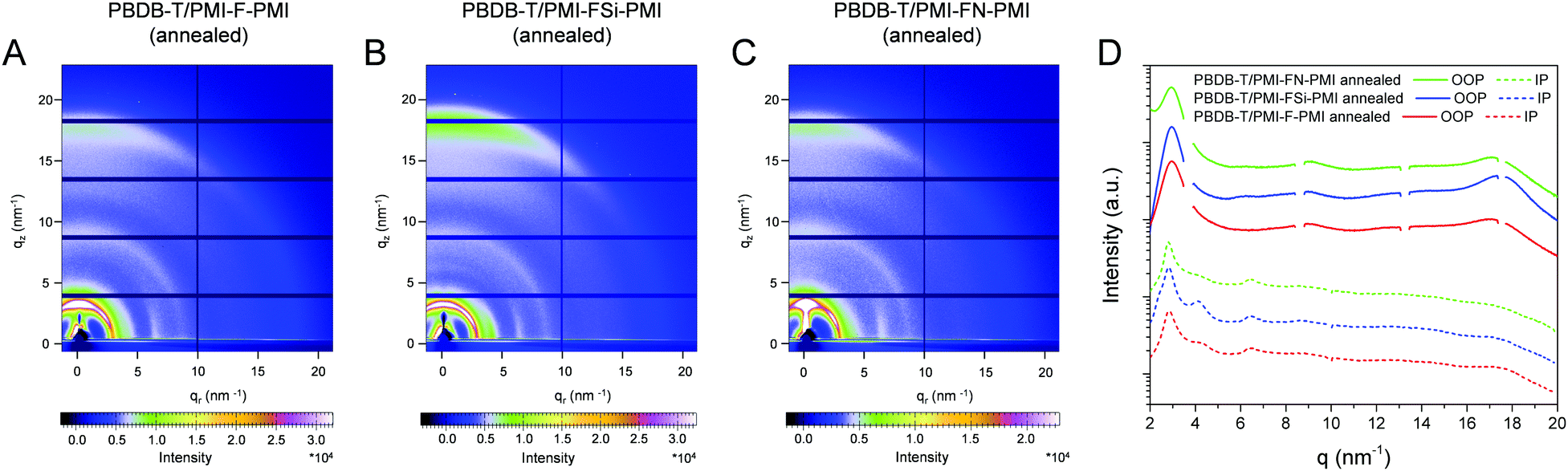 | ||
| Fig. 5 2D-GIWAXS patterns of donor/acceptor blends with a ratio of 1/1 for: (A) PMI-F-PMI (3a), (B) PMI-FSi-PMI (3b) and (C) PMI-FN-PMI (3c) w. annealing and (D) 1D-line cuts in the in-plane (IP) and out-of-plane (OOP) directions. The scattering profiles are shifted vertically for better visibility. | ||
Photovoltaic performance
Solar cells with the three synthesized NFAs – PMI-F-PMI, PMI-FSi-PMI and PMI-FN-PMI – were fabricated using an inverted device architecture – glass/ITO/ZnO/absorber/MoO3/Ag (Fig. 6A).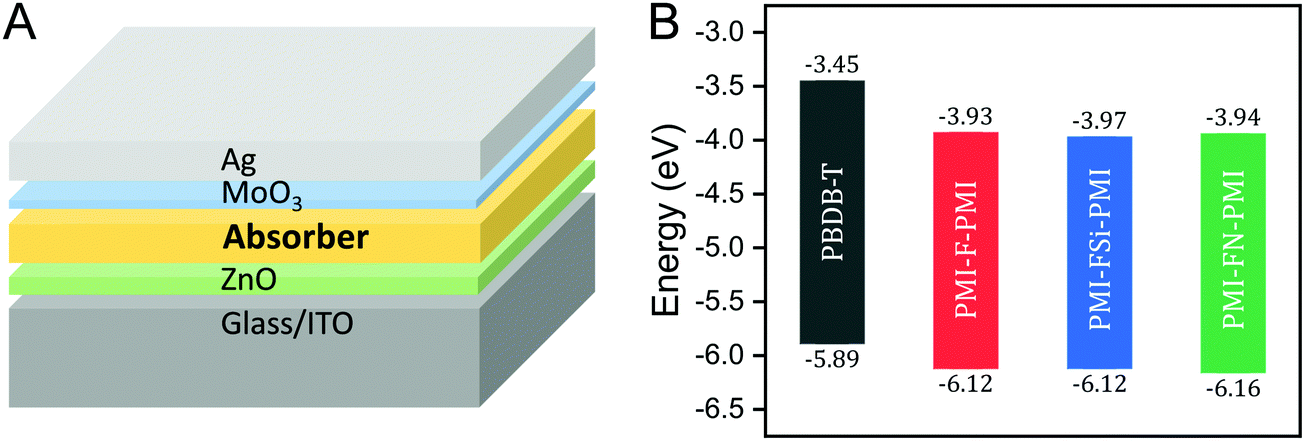 | ||
| Fig. 6 (A) Device architecture of the fabricated solar cells and (B) energy diagram of PMI-F-PMI (3a), PMI-FSi-PMI (3b), PMI-FN-PMI (3c) and PBDB-T. The HOMO/LUMO levels were determined by cyclic voltammetry. | ||
The donor/acceptor (D/A) blends were mixed in CB and spin coated at 70 °C in a two-step spin coating process to form a homogenous film. Solar cells with different D/A ratios of 1/0.66, 1/1 and 1/1.5 (w/w) were fabricated and their influence on solar cell performance was investigated. Herein, solar cells with a D/A ratio of 1/0.66 showed the highest power conversion efficiencies of 3.48%, 3.06% and 3.46% for PMI-F-PMI, PMI-FSi-PMI and PMI-FN-PMI, respectively (Table 3). For all solar cells, high VOCs between 1.05 and 1.10 V were obtained.
| Compound | Annealing temperature (°C) | Thickness (nm) | V OC (V) | J SC (mA cm−2) | FF (%) | PCE (%) |
|---|---|---|---|---|---|---|
| PMI-F-PMI | ||||||
| Best cell | — | 93 | 1.10 | 7.04 | 45.4 | 3.48 |
| Average | 88 ± 3.7 | 1.06 ± 0.03 | 6.54 ± 0.28 | 44.7 ± 1.7 | 3.09 ± 0.18 | |
| Best cell | 135 | 85 | 1.10 | 8.94 | 52.9 | 5.16 |
| Average | 93 ± 6.7 | 1.09 ± 0.04 | 8.13 ± 0.47 | 48.8 ± 2.9 | 4.34 ± 0.37 | |
| PMI-FSi-PMI | ||||||
| Best cell | — | 88 | 1.08 | 6.58 | 43.4 | 3.06 |
| Average | 92 ± 13 | 1.05 ± 0.05 | 6.08 ± 0.33 | 42.4 ± 1.7 | 2.69 ± 0.15 | |
| Best cell | 150 | 78 | 1.14 | 8.55 | 53.4 | 5.16 |
| Average | 75 ± 2.4 | 1.12 ± 0.02 | 7.88 ± 0.42 | 53.1 ± 1.5 | 4.67 ± 0.28 | |
| PMI-FN-PMI | ||||||
| Best cell | — | 80 | 1.08 | 8.17 | 39.6 | 3.46 |
| Average | 90 ± 7.6 | 1.08 ± 0.03 | 7.08 ± 0.30 | 40.1 ± 1.9 | 3.07 ± 0.15 | |
| Best cell | 150 | 78 | 1.06 | 10.18 | 48.0 | 5.16 |
| Average | 81 ± 13 | 1.11 ± 0.04 | 9.10 ± 0.62 | 44.2 ± 2.6 | 4.45 ± 0.36 | |
In addition, the respective J–V curves and the characteristic parameters of solar cells with D/A ratios of 1/1 and 1/1.5 are summarized in the ESI† (Fig. S17A, B and Table S2). It should be noted that upon increasing the ratio of the acceptor, a decreased current density and fill factor are the main cause for the decrease in device performance, which can be ascribed to an unbalanced charge transport and the slightly thicker absorber layers in these solar cells.
To further increase the device performance, the absorber layers with a D/A ratio of 1/0.66 were thermally annealed directly after spin coating. Two annealing temperatures (135 and 150 °C, annealing time: 5 min) were chosen, as the glass transition temperature of PBDB-T was found to be in the range of 145 °C (the corresponding DSC data are plotted in Fig. S18, ESI†). Indeed, using such an annealing step leads to an increase of the overall performance. While for PMI-F-PMI based solar cells an annealing temperature of 135 °C led to the best PCEs, for the PMI-FSi-PMI and PMI-FN-PMI based devices, the best performance was obtained upon annealing at 150 °C. J–V curves of the best solar cells (non-annealed and annealed) measured under illumination and in dark conditions are depicted in Fig. 7A–C and their solar cell characteristics are given in Table 3 and Table S3 (ESI†). Noticeable, the current density increased by 1–2 mA cm−2 due to the annealing step and the highest current density (10.18 mA cm−2) was obtained for the PBDB-T/PMI-FN-PMI-based solar cell. Moreover, the fill factors of the solar cells with all three NFAs could also be significantly enhanced due to an increased crystallinity in the absorber layer. This results in maximum device efficiencies of 5.16% for the PMI-F-PMI-based solar cells annealed at 135 °C and for the PMI-FSi-PMI and PMI-FN-PMI-based solar cells annealed at 150 °C.
 | ||
| Fig. 7 J–V curves (under illumination – solid symbols and under dark conditions – hollow symbols; notice that the hollow curves overlay) and EQE spectra of the best solar cells of PBDB-T: (A and D) PMI-F-PMI (3a), (B and E) PMI-FSi-PMI (3b) and (C and F) PMI-FN-PMI (3c) with a D/A ratio of 1/0.66 w. and w/o annealing of the absorber. | ||
External quantum efficiency (EQE) spectra of PMI-F-PMI, PMI-FSi-PMI and PMI-FN-PMI based solar cells with a D/A ratio of 1/0.66 (non-annealed and annealed) are depicted in Fig. 7D–F. The EQE spectra show an onset of photocurrent generation at 700 nm corresponding to the absorption onset of PBDB-T. Moreover, the photoresponse of the EQE spectra matches well with the absorption spectra of the blend films revealing a contribution of donor and acceptor component to charge carrier generation. The pronounced broad shoulder around 630 nm matches with the absorption maximum of the conjugated polymer and the maxima of the EQE spectra are in line with the maxima of the absorption spectra of the new acceptors. Moreover, in the EQE spectra of the solar cells prepared with D/A ratios of 1/1 and 1/1.5 (see Fig. S17C and D, ESI†) the increased acceptor content in the absorber layer leads to an increased photocurrent generation in the spectral region in which the PMI-based acceptors show strong absorption, compared to the wavelength region above 600 nm where the photocurrent generation is based on absorption in PBDB-T – the donor component in the absorber layer (cf. absorption spectra in Fig. S19, ESI†).
The current densities calculated from the EQE data match well with current densities from the J–V measurements performed either before or after the EQE measurements (Table S4, ESI†). As these measurements were performed in ambient atmosphere, slightly reduced JSC values were observed after the EQE measurements. As expected, for the devices annealed at 135 or 150 °C, respectively, increased EQE values were obtained. Herein the annealed solar cells with the PMI-F-PMI, PMI-FSi-PMI and PMI-FN-PMI acceptors (D/A ratio of 1/0.66) showed maximum EQE values of 53%, 53% and 57%, respectively.
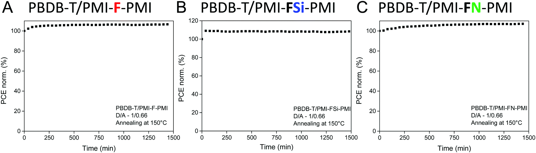
Moreover, the stability of the solar cells (D/A ratio 1/0.66, annealing at 150 °C) was investigated. Therefore, solar cells with device efficiencies close to the average values mentioned in Table 3 were selected for maximum power point (MPP) tracking under continuous illumination and active load for 24 hours. As can be seen in Fig. 8, the solar cells reveal a stable output over 24 h. The device performance even increased slightly and for all three solar cells more than 100% of their initial device efficiency were found after the testing period. The main part of the increase in PCE occurred during the first 60 minutes, which most likely stems from an increased conductivity of the ZnO layer due to light soaking.43
 | ||
| Fig. 8 Maximum power point tracking of solar cells with the PBDB-T/acceptor absorber layers: (A) PMI-F-PMI (3a), (B) PMI-FSi-PMI (3b) and (C) PMI-FN-PMI (3c) (D/A – 1/0.66, annealed at 150 °C), measured for 24 h under inert conditions. | ||
Film morphology
Since annealing of the solar cells strongly improved the photovoltaic performance, AFM measurements were performed on not annealed and annealed samples in order to investigate possible morphological changes of the organic semiconductor surface. The AFM images of the absorber layers of the solar cells with D/A ratios of 1/0.66 processed without annealing, as well as post-annealed devices at 135/150 °C are presented in Fig. 9.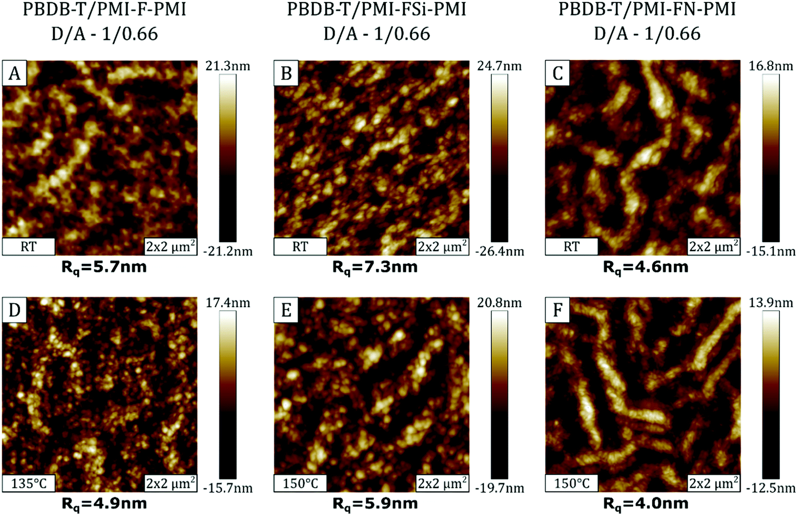 | ||
| Fig. 9 2 × 2 μm2 AFM images of as cast and post-annealed solar cell devices. The images in the first row (A–C) depict the surface of the absorber layers without thermal annealing, while in the second row (D–F) the images of the annealed samples are presented. | ||
The AFM topography images of the PBDB-T/PMI-F-PMI and PBDB-T/PMI-FSi-PMI samples (Fig. 9A and B) are characterized by a surface morphology consisting of a spheroidal structure with small domains. In the non-annealed PBDB-T/PMI-FN-PMI absorber layer (Fig. 9C), the spheroidal structure is superimposed by a fiber-like surface morphology. Regarding the surface roughness, Rq values of ∼4–6 nm are found in the PBDB-T/PMI-F-PMI and PBDB-T/PMI-FN-PMI samples and the PBDB-T/PMI-FSi-PMI sample, in which the crystallization of the acceptor is more pronounced, exhibited higher Rq values of 7–8 nm.
The AFM images of the absorber layer of the devices, which have been heat treated at 135/150 °C, are shown in Fig. 9D–F. Morphology-wise there are no significant differences between the annealed and non-annealed absorber layers based on PMI-F-PMI and PMI-FSi-PMI, However, in the PBDB-T/PMI-FN-PMI sample the fiber-like structure is distinctly more pronounced. Regarding the surface roughness, the annealing process tends to reduce the Rq values for all three absorber layers. However, the change is quite subtle and influences of other effects like local morphology variations cannot be excluded.
Conclusion
Three different perylene monoimide non-fullerene acceptors bridged via fluorene, silafluorene and carbazole linkers – PMI-F-PMI, PMI-FSi-PMI and PMI-FN-PMI – were synthesized via Suzuki coupling. DFT calculations displayed suitable HOMO/LUMO levels for the application as acceptors in organic solar cells and a 55° dihedral angle between the PMI units and the linkers. This twisting together with the long alkyl chains on the central linker unit as well as the diisopropylphenyl substituents on the PMI part helps to avoid pronounced π–π-stacking and leads to an excellent solubility. The three A–D–A type acceptors exhibit an absorption maximum at around 530 nm, absorption coefficients of 9 × 10⁴ M−1 cm−1 and good fluorescence quantum yields (∼70%). It was found that the introduction of the heteroatoms in the fluorene-derivative linker does not significantly influence the electronic properties such as HOMO/LUMO levels or charge carrier mobilities. A distinct difference was, however, observed regarding structural properties as GIWAXS measurements revealed that the crystallinity of PMI-FSi-PMI is significantly more pronounced compared to the other two investigated acceptors. Interestingly, these differences in crystallinity and molecular packing do not substantially influence the performance of the organic solar cells, which were fabricated in an inverted device setup using the conjugated polymer PBDB-T as donor material. The solar cells based on all three acceptors show similar device performances. The highest PCEs were obtained using a D/A ratio of 1/0.66 (w/w). Thermal annealing of the absorber layers leads to increased crystallinity of the absorber layers, which is also reflected in increased device efficiencies up to 5.16%.Experimental
Materials and methods
All reagents and solvents were purchased from commercially available sources (Sigma Aldrich, Lumtec, abcr, VWR, Roth) and used as received.Synthetic procedures
The synthesis of PMI and PMI-Br were performed and verified according to literature procedures.44,45PMI-F-PMI, PMI-FSi-PMI and PMI-FN-PMI were synthesized under standard Suzuki-coupling conditions in toluene with Pd(PPh3)4 catalyst. The detailed synthesis procedures are given in the ESI.†Fabrication of solar cells
Patterned glass/ITO substrates (15 × 15 × 1.1 mm3) (15 Ω sq−1) from Luminescence Technology Corp. were precleaned with acetone, put in an isopropyl alcohol bath, and placed into an ultrasonic bath at 40 °C for 30 min. The substrates were then dried with N2 and plasma etched for 3 minutes. The zinc oxide precursor solution was prepared by dissolving 500 mg zinc acetate dihydrate in 5 ml 2-methoxyethanol and 150 μl ethanolamine and stirring for 8 hours, followed by filtration (0.45 μm PVDF filter). The precursor solution was spin coated at 4000 rpm for 30 s and afterwards annealed at 150 °C for 15 minutes in air. The donor/acceptor solutions were prepared in an N2 filled glove box with D/A weight ratios of 1/0.66, 1/1 and 1/1.5. The concentration of the donor PBDB-T was kept constant at 10 mg ml−1 (solvent: chlorobenzene) and the amount of the acceptor was adjusted according to the envisaged D/A weight ratio. The blend solutions were stirred at 50 °C over night. Before applying the blend, the solution was heated to 70 °C for 30 minutes and then hot spin coated (70 °C) on the zinc oxide layer. A two-step spin coating process was used to achieve layer thicknesses around 100 nm (first step) and to dry the substrate (5000 rpm/5 s) (second step). A part of the samples was annealed at 135 °C or 150 °C for 5 min. Therefore, the heating plate was thoroughly calibrated using a PT100 temperature sensor mounted on a glass/ITO substrate prior to the annealing experiments. The solar cells were completed by thermal evaporation of MoO3 (10 nm) and Ag (100 nm) under high vacuum conditions (1 × 10⁻⁵ mbar).Characterization techniques
NMR spectroscopy (1H, APT) was performed on a Bruker Avance 300 MHz and/or Varian Inova 500 MHz spectrometers. Chemical shifts were referenced to tetramethylsilane (TMS – 0.00 ppm) or a solvent peak (CDCl313C 77.16 ppm). Deuterated chloroform-d with 0.03% TMS was obtained from Cambridge Isotope Laboratories Inc.MALDI-TOF mass spectrometry was performed on a Micromass TofSpec 2E time-of flight mass spectrometer. The instrument was equipped with a nitrogen laser (λ = 337 nm, operated at a frequency of 5 Hz) and a time lag focusing unit. Ions were generated just above the threshold laser power. Positive ion spectra were recorded in reflection mode with an accelerating voltage of 20 kV. The spectra were externally calibrated with a polyethylene glycol standard. Data analysis was done with MassLynx-Software V3.5 (Micromass/Waters, Manchester, UK). Samples were dissolved in dichloromethane (c = 1 mg ml−1). The matrix was either trans-2-[3-(4-tert-butylphenyl)-2-methyl-2-propenylidene]malononitrile (DCTB) or dithranol (c = 10 mg ml−1). Sample and matrix were mixed in a ratio of 2![[thin space (1/6-em)]](https://www.rsc.org/images/entities/char_2009.gif) :7 and was spotted onto the target and allowed to air-dry.
:7 and was spotted onto the target and allowed to air-dry.
Decomposition temperatures were determined using a Netzsch Jupiter STA 449C thermogravimetric analyzer in aluminium crucibles under helium atmosphere with a flow rate of 50 mL min−1. The operated temperature range was between 20–550 °C with a heating rate of 10 °C min−1. Differential scanning calorimetry (DSC) was performed on a DSC 8500 (PerkinElmer USA) using heating rates of 20 °C min−1 and 40 °C min−1 under nitrogen atmosphere, with a flowrate of 20 mL min−1. Glass-transition temperatures (Tg) from the second heating run were interpreted as the midpoint of change in heat capacity. The samples (3–10 mg) were measured in aluminium pans.
Computations were done using Gaussian09 software.39 Ground state minimal energy was localized, followed by its verification with frequency calculation (B3LYP level of theory, 6-31G* basis set). Excitation energy was calculated using TD-DFT (B3LYP, 6-31+G*).
Absorption spectra were recorded on a Shimadzu spectrophotometer UV-1800 (300 to 1000 nm). Spectra of solutions were recorded in chloroform and for the measurements of thin film spectra samples on glass substrates were used. Fluorescence measurements were recorded in ambient atmosphere on a FluoroLog 3 spectrofluorometer from Horiba Scientific equipped with an NIR-sensitive R2658 photomultiplier from Hamamatsu (300–1050 nm). Compounds were measured in a solution of chloroform (c = 1 to 4 μmol l−1) and on glass substrates. Relative luminescence quantum yields were determined using Lumogen orange (Kremer Pigmente, Germany) as reference compound (ϕfl = 1.0 in CHCl3).46 Excitation and emission scans of the acceptor thin films were measured with a PTI QuantaMaster 40.
Cyclic voltammetry (CV) measurements of PBDB-T, PMI-F-PMI, PMI-FSi-PMI and PMI-FN-PMI were performed to determine their respective HOMO–LUMO energy levels using a Jaissle Potentiostat–Galvanostat IMP 88 PC-100. A standard three-electrode setup was used where an Ag/AgCl wire served as quasi-reference electrode and two Pt-plates served as working and counter electrodes. On a hotplate (50 °C) and in nitrogen atmosphere the investigated organic materials were deposited onto the working electrode via drop-casting. All CV measurements were performed in a nitrogen glovebox using 0.1 M tetrabutylammoniumhexafluorophosphate (TBAPF6) in acetonitrile (MeCN) as the electrolyte solution. The scan speed was 50 mV s−1. Two separate measurements on freshly drop-casted materials were carried out to determine the oxidation and reduction onset, respectively. In order to avoid the effect of possible trapped charges, measurements to determine the oxidation onset were cycled through starting from zero to positive voltages, whereas measurements to determine the reduction onset were cycled through starting from zero to negative voltages. Every measurement was externally calibrated by measuring the half-wave potential of a Fc/Fc+ redox couple. The HOMO and LUMO energy levels were calculated using the following equations:47
| EHOMO = −(4.75 + Eoxonsetvs.NHE) eV |
| ELUMO = −(4.75 + Eredonsetvs.NHE) eV |
OFET fabrication and characterization: as a first step, the OFET glass substrates were sonicated for 15 minutes in Hellmanex®, deionized water, acetone and isopropanol, followed by a 5 minute O2 plasma treatment (50 W). OFET devices were fabricated in a bottom-gate, top-contact geometry with aluminum top electrodes (source and drain) and an aluminum gate electrode covered with a thin, insulating oxide layer. The aluminum bottom-gate electrode was thermally evaporated through a shadow mask onto a pre-cleaned glass substrate under a base pressure of 2 × 10⁻⁶ mbar until a thickness of 100 nm was reached. Subsequently, electrochemical anodization was used to grow a 32 nm dielectric Al2O3 layer. The Al gate electrode is immersed into a 0.01 M electrolyte solution of citric acid/trisodium citrate in ultrapure 18 MΩ water (0.265 g/2.57 g in 100 ml H2O) and serves as working electrode.49 A Pt-foil is placed parallel to the substrate, which acts as a counter electrode. Applying a constant voltage of 20 V for several minutes leads to the formation of a 32 nm thick oxide layer, due to an oxide formation factor of 1.6 nm V−1 for this electrolyte system.50
As a next step, the substrates were rinsed thoroughly with 18 MΩ water, dried and transferred into a nitrogen filled glovebox, where a thin passivation layer of benzocyclobutene (BCB) (1:50 diluted in mesitylene) was spin-coated at 25 rps for 45 seconds. Typical film thicknesses of the BCB layers were between 10–15 nm. Afterwards, the substrates were annealed at 280 °C for 1 hour on a hotplate in nitrogen atmosphere in order to cure the BCB layer.
The organic semiconductor materials (PMI-F-PMI, PMI-FSi-PMI and PMI-FN-PMI) were spin-coated on top of the BCB layer under nitrogen atmosphere with a two-step spin-coating recipe of 20 rps for 10 s followed by 67 rps for 20 s. As a final step, Al source and drain top electrodes were thermally evaporated on top of the semiconductor using a shadow mask. Evaporation conditions were the same as described for the gate electrode. The evaporation mask geometry of source, drain and gate electrodes results in transistors with a channel width W of 2000 μm and a channel length L of 65 μm.
OFET devices were measured in a nitrogen filled glove box with an Agilent B1500A semiconductor device parameter analyzer. Transistor transfer curves were measured by sweeping the gate voltage from 0 to 10 V and back to 0 V in 50 mV steps. After each sweep the drain voltage was increased by 2 V until a final drain voltage of 10 V was reached.
The surface morphology of the active layer of the solar cell devices was characterized with a Brucker Innova AFM. Measurements were carried out in tapping mode and under ambient conditions.
2D grazing incidence wide angle X-ray scattering (GIWAXS) measurements were performed at the Austrian SAXS Beamline 5.2L of the electron storage ring ELETTRA Trieste at a photon energy of 8 keV.51 For the detection of the GIWAXS images, a Dectris Pilatus3 1M detector was used set to a sample detector distance of 294 mm. The angular calibration of the detector was carried out using silver behenate powder (d-spacing: 58.38 Å). All measurements have been performed with a grazing angle of 0.17°. The in-plane cuts taken at the Yoneda wing (qr) and out-of-plane cuts (qz) along the Ewald sphere have been determined with the data evaluation software SAXS Dog.
Surface profilometry measurements were performed on a Bruker DektakXT stylus surface profiling system equipped with a 12.5 μm-radius stylus tip. Line scans were recorded over a length of 500 μm, with a stylus force of 3 mg, and a resolution of 0.33 μm pt−1. The layer thicknesses were determined from two-dimensional surface profiles using Vision 64 software (Bruker).
J–V curves of all devices were recorded inside a glovebox (nitrogen atmosphere) with a scan rate of 200 mV s−1 using a Keithley 2400 source meter connected to a LabView-based software. Illumination (100 mW cm−2) was provided by a Dedolight DLH400 lamp, calibrated using a monocrystalline silicon WPVS reference solar cell from Fraunhofer ISE. The active area of the solar cells was defined by a shadow mask (2.65 × 2.65 mm) used for the illumination. External quantum efficiency (EQE) measurements were acquired using a MuLTImode 4-AT monochromator (Amko) equipped with a 75 W xenon lamp (LPS 210-U, Amko), a lock-in amplifier (Stanford Research Systems, Model SR830), and a Keithley 2400 source meter. The monochromatic light was chopped at a frequency of 30 Hz, and constant background illumination was provided by white light LEDs. The EQE spectra were measured in the wavelength range of 380–900 nm (increment: 10 nm). The measurement setup was spectrally calibrated with a silicon photodiode (818-UV/DB, Newport Corporation). The MPP tracking tests of the solar cells were performed under continuous illumination with a white light (6500 K) 10 W chip-on-board high power LED.
Conflicts of interest
There are no conflicts of interest to declare.Acknowledgements
Financial support by the Austrian “Climate and Energy Fund” within the program Energy Emission Austria (Project: ALTAFOS, FFG No. 865 072) is gratefully acknowledged. The authors thank Efthymia Vakalopoulou, Josefine Hobisch, Petra Kaschnitz and Karin Bartl for experimental support. Moreover, the authors acknowledge the CERIC-ERIC Consortium for the access to experimental facilities (Austrian SAXS beamline at Elettra Sincrotrone Trieste) and financial support.References
- S. Günes, H. Neugebauer and N. S. Sariciftci, Chem. Rev., 2007, 107, 1324–1338 CrossRef.
- Y. Lin and X. Zhan, Acc. Chem. Res., 2016, 49, 175–183 CrossRef CAS.
- Y. Liu, J. Zhao, Z. Li, C. Mu, W. Ma, H. Hu, K. Jiang, H. Lin, H. Ade and H. Yan, Nat. Commun., 2014, 5, 5293 CrossRef CAS.
- J. Zhao, Y. Li, G. Yang, K. Jiang, H. Lin, H. Ade, W. Ma and H. Yan, Nat. Energy, 2016, 1, 15027 CrossRef CAS.
- G. Sauvé and R. Fernando, J. Phys. Chem. Lett., 2015, 6, 3770–3780 CrossRef.
- C. B. Nielsen, S. Holliday, H.-Y. Chen, S. J. Cryer and I. McCulloch, Acc. Chem. Phys., 2015, 48, 2803–2812 CrossRef CAS.
- H. Kang, W. Lee, J. Oh, T. Kim, C. Lee and B. J. Kim, Acc. Chem. Res., 2016, 49, 2424–2434 CrossRef CAS.
- X. Liu, B. Xie, C. Duan, Z. Wang, B. Fan, K. Zhang, B. Lin, F. J. M. Colberts, W. Ma, R. A. J. Janssen, F. Huang and Y. Cao, J. Mater. Chem. A, 2018, 6, 395–403 RSC.
- X. Li, K. Wu, L. Zheng, Y. Deng, S. Tan and H. Chen, Dyes Pigm., 2019, 168, 59–67 CrossRef CAS.
- P. S. Rao, V. G. More, A. D. Jangale, S. V. Bhosale, R. S. Bhosale, A. L. Puyad, J.-Y. Chen, J.-L. Li, S. V. Bhosale, A. Gupta and G. D. Sharma, Dyes Pigm., 2019, 171, 107677 CrossRef CAS.
- J. Yang, F. Chen, P. Cong, H. Xiao, Y. Geng, Z. Liao, L. Chen, B. Zhang and E. Zhou, J. Energy Chem., 2020, 40, 112–119 CrossRef.
- H. Yin, S. Chen, P. Bi, X. Xu, S. H. Cheung, X. Hao, Q. Peng, X. Zhu and S. K. So, Org. Electron., 2019, 65, 156–161 CrossRef CAS.
- Y. Cui, H. Yao, J. Zhang, T. Zhang, Y. Wang, L. Hong, K. Xian, B. Xu, S. Zhang, J. Peng, Z. Wei, F. Gao and J. Hou, Nat. Commun., 2019, 10, 2515 CrossRef.
- G. Xie, Z. Zhang, Z. Su, X. Zhang and J. Zhang, Nano Energy, 2020, 69, 104447 CrossRef CAS.
- B. Fan, D. Zhang, M. Li, W. Zhong, Z. Zeng, L. Ying, F. Huang and Y. Cao, Sci. China: Chem., 2019, 62, 746–752 CrossRef CAS.
- Y. Wu, Y. Zheng, H. Yang, C. Sun, Y. Dong, C. Cui, H. Yan and Y. Li, Sci. China: Chem., 2020, 63, 265–271 CrossRef CAS.
- M. A. Green, E. D. Dunlop, J. Hohl-Ebinger, M. Yoshita, N. Kopidakis and A. W. Y. Ho-Baillie, Prog. Photovoltaics Res. Appl., 2020, 28, 3–15 CrossRef.
- C. W. Tang, Appl. Phys. Lett., 1986, 48, 183–185 CrossRef CAS.
- Z. Luo, K. Wu, Y. Zhao, B. Qiu, Y. Li and C. Yang, Dyes Pigm., 2019, 163, 356–362 CrossRef CAS.
- J. Cheng, B. Li, X. Ren, F. Liu, H. Zhao, H. Wang, Y. Wu, W. Chen and X. Ba, Dyes Pigm., 2019, 161, 221–226 CrossRef CAS.
- J. Liu, S. Chen, D. Qian, B. Gautam, G. Yang, J. Zhao, J. Bergqvist, F. Zhang, W. Ma, H. Ade, O. Inganäs, K. Gundogdu, F. Gao and H. Yan, Nat. Energy, 2016, 1, 16089 CrossRef CAS.
- Y. Yang, Y. Wang, Y. Xie, T. Xiong, Z. Yuan, Y. Zhang, S. Qian and Y. Xiao, Chem. Commun., 2011, 47, 10749–10751 RSC.
- X. Lian, L. Zhang, Y. Hu, Y. Zhang, Z. Yuan, W. Zhou, X. Zhao and Y. Chen, Org. Electron., 2017, 47, 72–78 CrossRef CAS.
- M. B. A. Qureshi, M. Li, H. Wang, J. Song and Z. Bo, Dyes Pigm., 2020, 173, 107970 CrossRef.
- A. G. Macedo, L. P. Christopholi, A. E. X. Gavim, J. F. de Deus, M. A. M. Teridi, A. R. bin, M. Yusoff and W. J. da Silva, J. Mater. Sci.: Mater. Electron., 2019, 30, 15803–15824 CrossRef CAS.
- V. Kamm, G. Battagliarin, I. A. Howard, W. Pisula, A. Mavrinskiy, C. Li, K. Müllen and F. Laquai, Adv. Energy Mater., 2011, 1, 297–302 CrossRef CAS.
- A. Wadsworth, M. Moser, A. Marks, M. S. Little, N. Gasparini, C. J. Brabec, D. Baran and I. McCulloch, Chem. Soc. Rev., 2018, 48, 1596–1625 RSC.
- J. Zhang, H. S. Tan, X. Guo, A. Facchetti and H. Yan, Nat. Energy, 2018, 3, 720–731 CrossRef CAS.
- J. Zhang, Y. Li, J. Huang, H. Hu, G. Zhang, T. Ma, P. C. Y. Chow, H. Ade, D. Pan and H. Yan, J. Am. Chem. Soc., 2017, 139, 16092–16095 CrossRef CAS.
- G. Zhang, J. Feng, X. Xu, W. Ma, Y. Li and Q. Peng, Adv. Funct. Mater., 2019, 29, 1906587 CrossRef CAS.
- F. Tang, K. Wu, Z. Zhou, G. Wang, B. Zhao and S. Tan, ACS Appl. Energy Mater., 2019, 2, 3918–3926 CrossRef CAS.
- Y. Li, M. Han, W. Yang, J. Guo, K. Chang, J. Wang, J. Min, Q. Li and Z. Li, Mater. Chem. Front., 2019, 3, 1840–1848 RSC.
- R. Qin, D. Guo, T. Y. Gopalakrishna, G. Li, J. Yang, Y. Jiang and H. Ma, Dyes Pigm., 2019, 160, 540–545 CrossRef CAS.
- D. Xia, F. Yang, J. Li, C. Li and W. Li, Mater. Chem. Front., 2019, 3, 1565–1573 RSC.
- J. Cremer and P. Bäuerle, Eur. J. Org. Chem., 2005, 3715–3723 CrossRef CAS.
- Y. Hu, S. Chen, L. Zhang, Y. Zhang, Z. Yuan, X. Zhao and Y. Chen, J. Org. Chem., 2017, 82, 5926–5931 CrossRef CAS.
- Y. Zhang, Y. Xiao, Y. Xie, L. Zhu, D. Shi and C. Cheng, Org. Electron., 2015, 21, 184–191 CrossRef CAS.
- Y. Zhang, X. Guo, B. Guo, W. Su, M. Zhang and Y. Li, Adv. Funct. Mater., 2017, 27, 1603892 CrossRef.
- M. J. Frisch, G. W. Trucks, H. B. Schlegel, G. E. Scuseria, M. A. Robb, J. R. Cheeseman, G. Scalmani, V. Barone, B. Mennucci, G. A. Petersson, H. Nakatsuji, M. Caricato, X. Li, H. P. Hratchian,A. F. Izmaylov, J. Bloino, G. Zheng, J. L. Sonnenberg, M. Hada, M. Ehara, K. Toyota, R. Fukuda, J. Hasegawa, M. Ishida, T. Nakajima, Y. Honda, O. Kitao, H. Nakai, T. Vreven, J. A. Montgomery, Jr., J. E. Peralta, F. Ogliaro, M. Bearpark, J. J. Heyd, E. Brothers, K. N. Kudin, V. N. Staroverov, T. Keith, R. Kobayashi, J. Normand, K. Raghavachari, A. Rendell, J. C. Burant, S. S. Iyengar, J. Tomasi, M. Cossi, N. Rega, J. M. Millam, M. Klene, J. E. Knox, J. B. Cross, V. Bakken, C. Adamo, J. Jaramillo, R. Gomperts, R. E. Stratmann, O. Yazyev, A. J. Austin, R. Cammi, C. Pomelli, J. W. Ochterski, R. L. Martin, K. Morokuma, V. G. Zakrzewski, G. A. Voth, P. Salvador, J. J. Dannenberg, S. Dapprich, A. D. Daniels, O. Farkas, J. B. Foresman, J. V. Ortiz, J. Cioslowski and D. J. Fox, Gaussian 09, Revision D.01, Gaussian, Inc., Wallingford CT, 2013 Search PubMed.
- J. Gierschner, J. Cornil and H. J. Egelhaaf, Adv. Mater., 2007, 19, 173–191 CrossRef CAS.
- H. Wu, H. Fan, S. Xu, C. Zhang, S. Chen, C. Yang, D. Chen, F. Liu and X. Zhu, Sol. RRL, 2017, 1, 1700165 CrossRef.
- Z. Zhang and X. Zhu, Chem. Mater., 2018, 30, 587–591 CrossRef CAS.
- X. Du, D. He, Z. Xiao and L. Ding, Synth. Met., 2012, 162, 2302–2306 CrossRef CAS.
- R. T. Cheriya, J. Joy, S. K. Rajagopal, K. Nagarajan and M. Hariharan, J. Phys. Chem. C, 2012, 116, 22631–22636 CrossRef CAS.
- F. Nolde, W. Pisula, S. Müller, C. Kohl and K. Müllen, Chem. Mater., 2006, 18, 3715–3725 CrossRef CAS.
- G. Seybold and G. Wagenblast, Dyes Pigm., 1989, 11, 303–317 CrossRef.
- C. M. Cardona, W. Li, A. E. Kaifer, D. Stockdale and G. C. Bazan, Adv. Mater., 2011, 23, 2367–2371 CrossRef CAS.
- N. G. Connelly and W. E. Geiger, Chem. Rev., 1996, 96, 877–910 CrossRef CAS.
- A. I. Mardare, M. Kaltenbrunner, N. S. Sariciftci, S. Bauer and A. W. Hassel, Phys. Status Solidi A, 2012, 209, 813–818 CrossRef CAS.
- M. Kaltenbrunner, P. Stadler, R. Schwödiauer, A. W. Hassel, N. S. Sariciftci and S. Bauer, Adv. Mater., 2011, 23, 4892–4896 CrossRef CAS.
- H. Amenitsch, M. Rappolt, M. Kriechbaum, H. Mio, P. Laggner and S. Bernstorff, J. Synchrotron Radiat., 1998, 5, 506–508 CrossRef CAS.
Footnote |
| † Electronic supplementary information (ESI) available. See DOI: 10.1039/d0ma00470g |
| This journal is © The Royal Society of Chemistry 2020 |