
 Open Access Article
 This Open Access Article is licensed under a Creative Commons Attribution-Non Commercial 3.0 Unported Licence
Aspect ratio controlled synthesis of tellurium nanowires for photovoltaic applications
Dipendra
Pokhrel
 ,
Ebin
Bastola
,
Adam B.
Phillips
,
Michael J.
Heben
and
Randy J.
Ellingson
*
,
Ebin
Bastola
,
Adam B.
Phillips
,
Michael J.
Heben
and
Randy J.
Ellingson
*
Wright Center for Photovoltaics Innovation and Commercialization, Department of Physics and Astronomy, The University of Toledo, Toledo, OH 43606, USA. E-mail: Randy.Ellingson@utoledo.edu
First published on 11th August 2020
Abstract
Here, we report an aspect ratio-controlled synthesis of tellurium (Te) nanowires (NWs) utilizing a hot-injection colloidal method. The synthetic method uses low cost materials – specifically, tellurium oxide (TeO2) as the tellurium source, environmentally benign ethylene glycol as a solvent, and ascorbic acid as a reducing agent. Analysis of scanning electron micrographs confirms that the NWs show narrow distributions for length, diameter, and therefore also aspect ratio. For example, we have prepared Te NWs exhibiting aspect ratios of 28.0 and 55.4. X-ray diffraction studies confirm a hexagonal crystal structure for the synthesized Te NWs. Based on Raman spectroscopy, Stokes lines were observed at 117.0 and 136.1 cm−1 for A1 and E2 modes of vibration. Fabrication of Te NW thin films demonstrated their suitability as a hole transport layer at the back contact of cadmium sulfide/cadmium telluride (CdS/CdTe) solar cells, yielding enhanced open-circuit voltage (Voc = 0.846 V) and fill factor (FF = 77.8%), and an efficiency of 14.6%; the control device has an efficiency of 13.1% (Voc = 0.825 mV, FF 74.0%).
Introduction
Nanomaterials offer significant value for opto-electronic applications because of their unique optical and electronic properties compared to their bulk counterparts.1–3 Properly prepared one-dimensional semiconductors, such as nanowires (NWs), possess superior axial transport properties (thermal and electrical conductivity) which make them applicable in opto-electronics including nano photonics and energy related applications.4,5 Tellurium (Te) is a rare earth element with narrow band gap energy (∼0.35 eV) and p-type conductivity.6 Te NWs often exhibit low defect density, enhanced thermoelectric performance, and photoconductivity.7–10 Here, we report on success in preparing controlled aspect ratio Te NWs, and demonstrate their use as a buffer layer for the back contact of cadmium telluride (CdTe) photovoltaic (PV) devices.Although Te nanostructures such as nanowires, nanorods and nanobelts can be prepared using solution-based and vacuum based approaches, these methods typically yield product with a wide size polydispersity, particularly in length. Solution-based techniques include solvothermal and hydrothermal approaches11–17 whereas for vacuum based technology include vapor deposition of Te such as thermal evaporation.18,19 Mohanty et al. have used thermal evaporation to produce Te NWs of several micron length with diameters of 100–300 nm.19 The solution-based approaches include the use of hydrazine as a reducing agent14,15,20 which is extremely hazardous and highly flammable. Thus, less hazardous and safer chemicals are desired for the synthesis of Te NWs. The solution-based synthesis gives a freedom for the solution-processing of the material for the fabrication of devices. Silva et al. yield the Te NWs with diameter less than 30 nm and lengths varying from 600 nm to 5 μm using hypophosphorous acid.21 Liu et al. have reported the rapid microwave assisted method to produce Te NWs with 20 nm diameter and length of tens of microns.8 In the synthesis of nanorods and nanowires, ascorbic acid is used as a reducing agent which is relatively less hazardous.11,22–24 Yang et al. reported the synthesis of Te NWs using ascorbic acid as a reducing agent and ethylene glycol as the solvent with average diameter of 9.7 ± 2.7 nm.24 Based on the literature, all these Te NWs have relatively uniform diameters but wide distribution of lengths. Uniform and controlled length of these Te NWs would provide an opportunity to improve the transport properties along the length. Thus, our novel strategy focuses on the synthesis of Te NWs with controlled aspect ratio, for application at the back-contact in CdTe solar cells.
Cadmium telluride is one of the leading cost-effective PV technologies for thin film solar cells with direct band gap energy of 1.5 eV and absorption coefficient >105 cm−1.25 In CdTe solar cells, the back contact interface layer plays a vital role in carrier transport, and the development of high-quality back contact is essential to improve the device performance.26 Due to its deep work function, preparation of low resistance and stable ohmic contact presents a major technology challenge for CdTe PV devices.27 To make a good contact and reduce the contact barrier and contact resistance on CdTe, several techniques have been employed such as back surface modification or insertion of a hole transport layer (HTL) between the CdTe and a metallic contact. The CdTe back surface can be modified by doping with Cu or etching the CdTe surface to create a Te-rich layer.28–30 The etching procedure generally consists of exposing the polycrystalline CdTe surface to an acidic alcoholic solution of bromine or iodine that selectively reacts with Cd atoms and leaves Te on the surface.31,32 Other (HTL) materials applied between CdTe and a metallic contact include iron pyrite, carbon nanotubes, copper doped ZnTe, nanocomposite (CuS)x(ZnS)1−x, and copper NWs with graphene.33–40 The formation or the deposition of Te layer is essential for the preparation of highly efficient CdTe photovoltaics. For example, the deposition of elemental Te by thermal evaporation has also improved the device performance.41 The use of length controlled Te NWs offers the important potential to develop point contacts at the back contact of p-type polycrystalline CdTe, in such a way as to allow for efficient hole extraction through an otherwise passivated interface.
Here, we report the synthesis and characterization of Te NWs with uniform length and diameter distributions using a colloidal hot injection method. During synthesis, tellurium oxide (TeO2) is the source of Te, L-ascorbic acid is used as a reducing agent, ethylene glycol as a solvent, and polyvinylpyrrolidone (PVP) serves as a surfactant. The synthesized Te NWs have hexagonal crystal structure with active vibrational modes at 117.0 and 136.1 cm−1 corresponding to A1 and E2 modes. Implementing these Te NWs to fabricate CdTe solar cell back contacts yield significantly improved open-circuit voltage (Voc) and fill factor (FF) compared to standard devices. The best cell using Te NWs has an efficiency of 14.6% (Voc 846 mV, FF 77.8%), an 11% improvement over the control device which converts at an efficiency of 13.1% (Voc 825 mV, FF 74.0%). These results are quite good for a film stack with CdS as the window layer, which limits the current density to about 75% of what can be obtained using a CdSe or MgZnOx front window layer.42
Experimental methods
Materials
Tellurium oxide (TeO2 ≥ 99%) was obtained from Alfa Aesar, polyvinylpyrrolidone (PVP, Molecular wt. ∼40![[thin space (1/6-em)]](https://www.rsc.org/images/entities/char_2009.gif) 000), L-ascorbic acid (≥99%) and ethylene glycol were obtained from Fisher Scientific, and potassium hydroxide (KOH ≥ 99%) was obtained from Sigma Aldrich are of analytical grade and used without further purification.
000), L-ascorbic acid (≥99%) and ethylene glycol were obtained from Fisher Scientific, and potassium hydroxide (KOH ≥ 99%) was obtained from Sigma Aldrich are of analytical grade and used without further purification.
Synthesis procedure
The synthesis of Te NWs is based on a slightly modified version of the procedure reported by Yang et al. previously.24 In a typical synthesis of Te NWs, 1.05 mmol (0.167 gm) of tellurium oxide (TeO2), 2.98 mmol (0.167 gm) of potassium hydroxide (KOH) and 0.1 gm of polyvinylpyrrolidone (PVP) were dissolved in 15 mL ethylene glycol (EG) under vigorous magnetic stirring to form a milky white solution. The temperature of the flask was set to 120 °C at which the solution becomes transparent yellow. In the meantime, 1.42 mmol (0.2496 gm) of ascorbic acid was dissolved in 0.75 mL of deionized water at 80 °C to form an aqueous ascorbic acid solution. When the reaction temperature reached to 120 °C, the ascorbic acid solution was rapidly injected resulting the change in color of the reactants to opaque black. The reaction was continued for 21 h at 120 °C in a dinitrogen (N2) environment to complete the synthesis of high quality Te NWs. The heating mantle was removed, and the flask temperature was lowered to room temperature using a cold-water bath. The product was centrifuged and cleaned with deionized water three to five times. The obtained NW product was dried and stored as a powder in a glove box in N2 environment for characterization and application.Tellurium NWs as a back-contact interface layer
To test Te NWs as a back contact to CdTe solar cells, we used CdS/CdTe film stacks deposited by Willard and Kelsey Solar Group, via vapor transport deposition (VTD) onto TECTM-15M (Pilkington N.A.) glass substrates. The CdTe devices were activated by CdCl2 treatment at 390 °C for 30 min in dry air environment to advance grain growth, release interfacial strain and facilitate intermixing at CdS/CdTe interface.43 The standard back contact was prepared using thermally evaporated copper (3 nm) and gold (40 nm) followed by annealing at 150 °C for 35 min. Similarly, a solution-based copper treatment was carried out using a procedure reported previously.44,45 To prepare devices using Te NWs as the HTL, 40 μL solution of Te NWs (10 mg mL−1) was dropped and spun onto the Cu-doped CdTe at 1000 and 3500 rpm for 10 and 50 s respectively. Devices were then annealed at 150 °C for 1 min, and Au (40 nm) was thermally evaporated to complete the back contact. The completed CdTe device was scribed using a 532 nm laser to produce approximately 24 cells of area 0.06 cm2.46Results and discussion
Synthesis and characterization of Te NWs
Fig. 1 displays the SEM images of Te NWs prepared with varying amounts of PVP and ascorbic acid. PVP acts as a structural directing agent and stabilizing agent,47 and therefore plays a vital role in the formation of Te NWs with uniform morphology. Along with PVP, the alkaline condition aids the growth of Te NWs. Fig. 1(a) and (b) shows the SEM images of Te NWs prepared using 0.1 gm of PVP and 0.75 mL of ascorbic acid solution. The synthesized Te NWs are uniform in length and diameter. Fig. 2(a) and (b) shows the diameter and length distribution of Te NWs with 0.1 gm of PVP and 0.75 mL of ascorbic acid.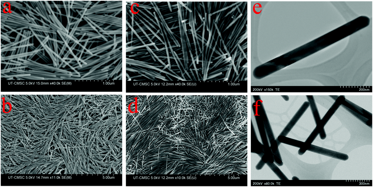 | ||
| Fig. 1 SEM images of Te NWs obtained from TeO2 with ethylene glycol at 120 °C (a) and (b) 0.1 gm PVP and 0.75 mL ascorbic acid (c) and (d) 0.2 gm PVP and 1.5 mL ascorbic acid and (e) and (f) STEM images of Te NWs obtained from 0.1 gm PVP and 0.75 mL ascorbic acid. | ||
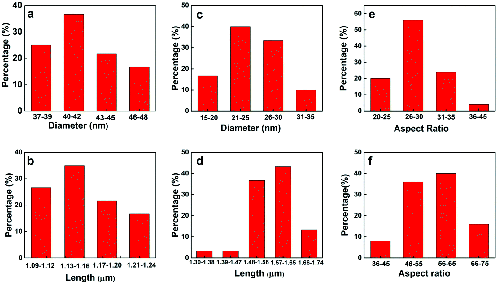 | ||
| Fig. 2 Diameter, length and aspect ratio distribuiton of Te NWs at 120 °C for 21 h. (a), (b) and (e) 0.1 g PVP and 0.75 mL ascorbic acid (c), (d) and (f) 0.2 g PVP and 1.5 mL ascorbic acid. | ||
From SEM image Fig. 1(a) and statistical analysis Fig. 2(a) and (b), the average length and diameter of the nanowires are 1.15 ± 0.03 μm and 41.0 ± 3.0 nm respectively. The Te NWs have very narrow size distribution with standard deviation ±0.03 μm in length and ±3.0 nm in diameter. In this case, the aspect ratio of Te NW is 28.0 ± 2.7. Upon increasing the amount of PVP to 0.2 g and ascorbic acid to 1.5 mL, Te NWs of uniform length and diameter were again obtained, however with decreased NW diameter and increased NW length. The SEM images are shown in Fig. 1(c) and (d). The average length and diameter of Te NWs are 1.54 ± 0.07 μm and 27.8 ± 3.7 nm respectively. The aspect ratio of Te NWs for this case is 55.4 ± 1.1. Fig. 2(c) and (d) shows the diameter and length distribution of Te NWs with 0.2 gm of PVP and 1.5 mL of ascorbic acid. Further, we calculated the aspect ratio of the individual NWs, and plotted the graphs for aspect ratios for two synthesis conditions as shown in Fig. 2(e) and (f). In case of the NWs synthesized by using 0.1 g PVP and 0.75 mL ascorbic acid, ∼56% of NWs have aspect ratio in the range of 26–30 while for 0.2 g PVP and 1.5 mL ascorbic acid, ∼40% of the NWs have aspect ratio in the range of 56–65 and ∼36% are in the range of 46–55. The increased in aspect ratio is due to the role of these PVP and ascorbic acid as directing agent and reducing agent.11Fig. 1(e) and (f) shows the scanning transmission electron microscope (STEM) images of Te NWs formed with 0.1 gm PVP and 0.75 mL ascorbic acid. It reveals that NWs are highly crystalline with uniform length and diameter. The unusual anisotropic crystal structure of Te consists of 1D helical chain of covalently bound atoms parallel to the c-axis.48 Previously, Zhong et al. used a solvothermal technique to synthesize Te NWs with diameter 30 ± 2 nm and length 10 ± 1 μm using ethylene glycol as a solvent.11 Qian et al. reported the synthesis of Te NWs with diameter 4–9 nm and lengths up to hundreds of μm and Wang et al. reported Te NWs with diameter 40 nm with lengths in several microns using hydrazine through hydrothermal method.14,15 In our case, we demonstrated the successful control of the aspect ratio of Te NWs, from 28.0 to 55.4, by varying the amount of ascorbic acid and PVP. The amount of surfactant and reducing agent are the key parameters to prepare the desired nanowires during synthesis. Potassium hydroxide to control alkalinity helps PVP to act fully as a surfactant for the synthesis of Te NWs. Here, we developed the Te NWs with uniform length and diameter using hot injection colloidal method with small deviation in length with standard deviations of 0.03 μm and 0.07 μm respectively for two cases.
Fig. 3(a) displays the typical XRD pattern of synthesized Te NWs performed in the ‘2θ’ range of 20–70°. The diffraction peaks obtained from MDI JADE closely match with the diffraction peaks measured for our as-synthesized Te NWs. Based on the standard powder diffraction file, synthesized Te NWs are in hexagonal phase with lattice constants a = b = 0.4454 nm and c = 0.5924 nm. The high intensity obtained in the diffraction pattern signifies the purity of the material. Similarly, Fig. 3(b) shows the Raman spectrum of Te NWs using a 632.8 nm He–Ne laser source with bands at 117.0, 136.1 and 265.9 cm−1. The mode with a vibration 117.0 cm−1 corresponds to A1 mode, 136.1 cm−1 corresponds to E2 mode and the bands at 265.9 cm−1 assigned to the second-order spectra of the Te NWs which agrees closely with previous reports.49,50
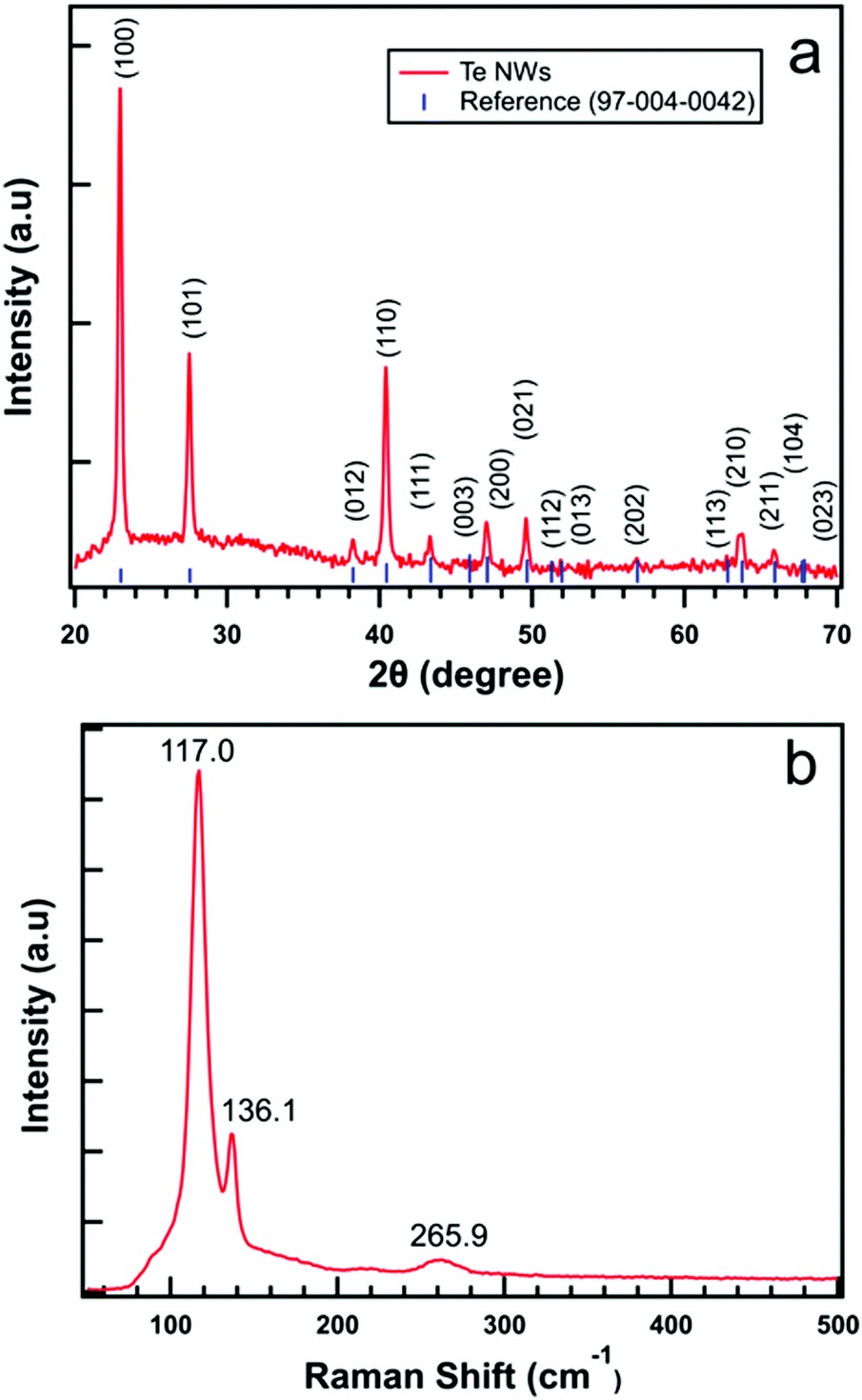 | ||
| Fig. 3 (a) X-ray diffraction pattern of synthesized Te NWs obtained from TeO2, possess hexagonal crystal structure and the sharp intensity peaks of the pattern indicate pure-phase crystalline material. The reference lines (PDF #97-004-0042) was obtained from MDI JADE software, and (b) Raman spectroscopy measurement of Te NWs using a 632.8 nm excitation from a He–Ne laser with 0.1 gm PVP and 0.75 mL ascorbic acid. | ||
Next, we investigated and analyzed the effect of Te NWs as a HTL on CdTe PV devices. Tellurium manifests as a p-type semiconductor, and has been reported with a majority carrier concentration of 2.65 × 1018 cm−3, Hall mobility of 8.99 cm2 V−1 S−1, and resistivity of 0.26 Ω cm.51 The insertion of a Te layer as a HTL on CdTe surface is to make a p/p+ interface with the CdTe absorber layer. The formation of Te on the back surface reduces the potential barrier height for hole transport between the CdTe and the back metal electrode.32Fig. 4 displays SEM images of the CdTe surface after CdCl2 treatment, (a) without and (b) with Te NWs applied. Fig. 4(b) clearly shows a CdTe surface covered with Te NWs. Fig. 4(c) shows the cross-sectional SEM image of CdS/CdTe solar cells with the Te NWs HTL and thickness of Te NWs layer is approximately 100 nm, and Fig. 4(d) shows the schematic diagram of the device structure.
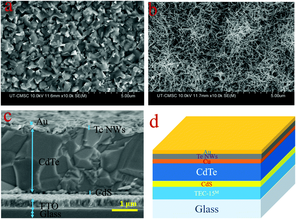 | ||
| Fig. 4 SEM images of CdCl2 treated CdTe (a) top surface w/o Te NWs and (b) top surface with Te NWs (c) cross-sectional image with Te NWs as HTL and (d) schematic diagram of the device structure. | ||
Fig. 5 shows the J–V characteristics and external quantum efficiencies (EQEs) of CdS/CdTe solar cells prepared with standard back contacts and prepared using Te NWs as an interface layer in between the Cu and Au. The back-contact designs tested here involved Cu/Au (evaporated metallic Cu), Cu/TeNWs/Au, CuCl2/Au (solution CuCl2), and CuCl2/TeNWs/Au. The solid and dashed lines correspond to light and dark measurements respectively. In the case of the Cu/Au back contact, the best device has an efficiency (η) of 13.1% with Voc 825 mV, Jsc 21.6 mA cm−2, and FF of 74.0%. When a Te NW film was used as the HTL (Cu/TeNWs/Au), the best device efficiency was 14.0% with a Voc of 837 mV, Jsc of 21.6 mA cm−2 and FF of 77.7%. For Cu/TeNWs/Au back contact devices, the average device efficiency was increased by about 7% as compared to Cu/Au back contacts with significant improvement on FF. Similarly, with solution-based copper (CuCl2/Au), the back contact, best cell has an efficiency (η) of 14.0% with Voc 841 mV, Jsc 22.1 mA cm−2, and FF of 75.4%. With Te NWs (CuCl2/TeNWs/Au), the best device efficiency was 14.6% with Voc of 846 mV, Jsc of 22.3 mA cm−2 and FF of 77.8%. We have observed that managing the Cu concentration and diffusion plays a critical role in performance, and we therefore believe that the use of CuCl2 solution to introduce the Cu enables better control than the thermal evaporation of a thin Cu layer.45 The average device efficiency was increased by about 4% as compared to the CuCl2/Au back contact. The average device parameters from twenty cells of each type of back contact are shown in Table 1. By introducing Te NWs as an interface layer, an improvement of open circuit voltage and fill factor was observed. The Jsc obtained from EQE measurement matches closely with Jsc obtained from J–V measurement.
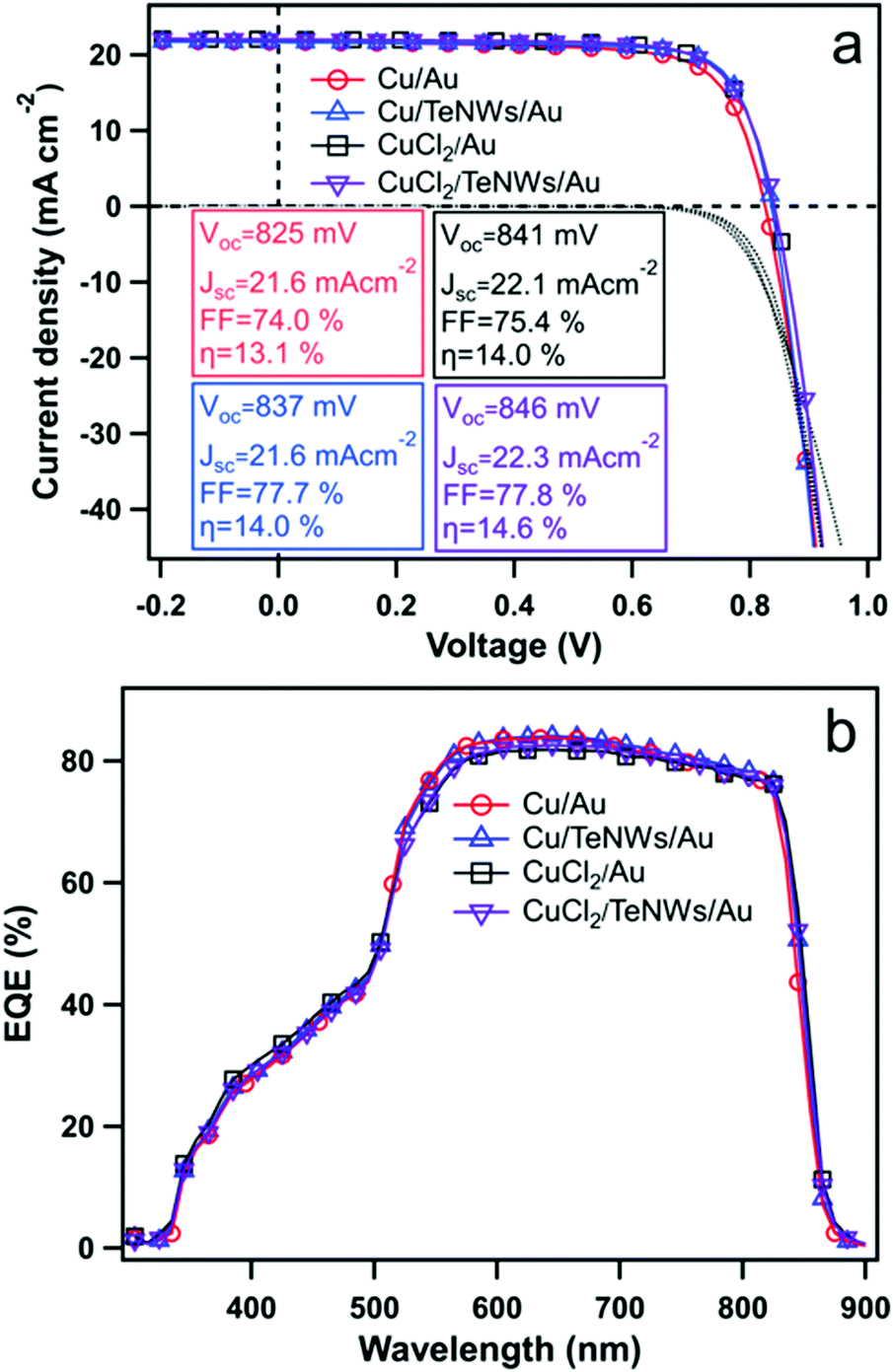 | ||
| Fig. 5 (a) J–V characteristics and (b) external quantum efficiency (EQE) of CdTe solar cells with Cu/Au, Cu/TeNWs/Au, CuCl2/Au and CuCl2/TeNWs/Au back contacts respectively. The solid and dotted lines in Fig. 5(a) represent J–V curves under illumination and dark conditions respectively. | ||
| Back-contacts | V oc (mV) | J sc (mA cm−2) | FF (%) | η (%) | R s (ohms cm2) | R shunt (ohms cm2) |
|---|---|---|---|---|---|---|
| Cu/Au | 818 ± 5 | 21.6 ± 0.3 | 72.8 ± 0.8 | 12.9 ± 0.2 | 3.5 ± 1.2 | 1737 ± 228 |
| Cu/TeNWs/Au | 835 ± 1 | 21.5 ± 0.1 | 77.3 ± 0.2 | 13.9 ± 0.1 | 3.8 ± 0.1 | 3504 ± 228 |
| CuCl2/Au | 838 ± 2 | 22.0 ± 0.1 | 74.8 ± 0.9 | 13.8 ± 0.2 | 4.3 ± 0.1 | 2983 ± 466 |
| CuCl2/TeNWs/Au | 844 ± 1 | 22.0 ± 0.2 | 77.2 ± 0.2 | 14.3 ± 0.1 | 4.0 ± 0.3 | 3781 ± 225 |
Tellurium as a buffer layer between CdTe and a metal contact has been shown to reduce the downward band bending and mitigate a Schottky barrier formed at the back contact.52 A Te buffer layer on CdTe can also be deposited by evaporation. Watthage et al. reported the best cell efficiency of 13.8% (Voc = 839 mV, and FF = 75.6%) and average efficiency of 13.3% with 80 nm thermally evaporated Te followed by 3 nm Cu and 40 nm Au.31 Previously, Liang et al. have also applied the Cu NWs with graphene as a back contact interface layer to CdTe photovoltaics, and they reported the device efficiency to be 12.1% while the control was 9.1% with Cu thin film.40 Similarly, Major et al. have used ZnO NWs instead of conventional ZnO thin film as a front contact material for CdTe solar cells. They reported photoconversion efficiency of 9.53% when using ZnO NWs, whereas use of a planar ZnO buffer layer had a device efficiency of 9.99%.53 Compared to these results, we observed >11% increase in device efficiency by using Te NWs compared to Cu/Au back contacts. Thus, a thin layer of Te NWs seems to be more effective to enhance the device efficiency which we attribute to the lowering of contact resistance and barrier height.
The J–V behavior of solar cells can be described by using single exponential diode equation as,
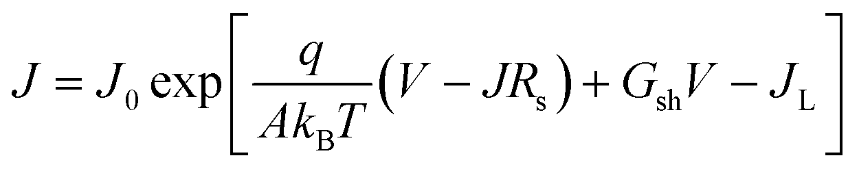 | (1) |
Fig. 6(a) displays dark J–V curves on a linear scale for various back contacts. In case of a Cu/Au back contact, we can see higher back barrier which explains the low fill factor of these cells compared to other back contacts. As evidenced from the dark J–V curves with Te NWs, we can see the improvement in the J–V behavior qualitatively. Fig. 6(b) shows the plot of dJ/dV versus bias voltage (V), and it indicates negligible shunt conductance (close to zero) in the devices under dark conditions. Thus, the term Gsh and JL were taken to be zero for these dark J–V curves. Similarly, Fig. 6(c) shows the plot of dV/dJ vs. J−1 from which we estimated the values of Rs and A. The values of the Rs and A were obtained from the y-intercept and slope of the linear fit as shown in the Fig. 6(c). Similarly, using these values of Rs, we plotted ln[J] versus [V–RsJ] as shown in Fig. 6(d) to estimate reverse saturation current density and ideality factor. The values of Rs, A and J0 for all back contacts obtained from Fig. 6 are presented in Table 2.
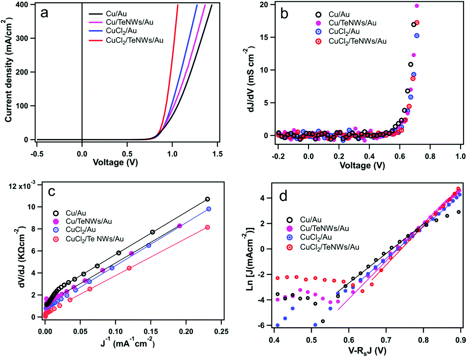 | ||
| Fig. 6 Analysis of dark J–V curves with back contacts Cu/Au, Cu/TeNWs/Au, CuCl2/Au and CuCl2/TeNWs/Au (a) dark J–V curve (b) shunt characterization (c) plot of dV/dJ versus l/J for calculation of A and Rs (d) plot of ln(J) versus V–RsJ for calculation of n and J0. The solid lines represent the corresponding fitted lines in (c) and (d). | ||
| Device parameters | Cu/Au | Cu/TeNWs/Au | CuCl2/Au | CuCl2/TeNWs/Au |
|---|---|---|---|---|
| A (dV/dJ vs. J−1) | 1.54 | 1.48 | 1.56 | 1.36 |
| R s (dV/dJ vs. J−1) (Ω cm2) | 1.83 | 1.21 | 0.76 | 0.48 |
|
A (lnJ vs. V–RsJ) |
1.60 | 1.35 | 1.44 | 1.3 |
|
J
0 (lnJ vs. V–RsJ) (mA cm−2) |
3.5 × 10⁻⁸ | 3.6 × 10⁻¹⁰ | 1.2 × 10⁻⁹ | 1.2 × 10⁻¹⁰ |
The value of A with Cu/Au back contact is about 1.54 while with Te NWs, its value is lowered to 1.48. Also, the reverse saturation current density (J0) is 3.5 × 10⁻⁸ mA cm−2 for Cu/Au and with Te NWs its value is 3.6 × 10⁻¹⁰ mA cm−2. The values of ideality factor and reverse saturation current are in close agreement with a previous report for CdS/CdTe device with standard back contact (Cu/Au).54 Similarly, the ideality factor and J0 are improved for CuCl2 treated devices with Te NWs. Thus, the interfacial layer helped to lower the value of the reverse saturation current density indicating better diode behavior of these CdS/CdTe solar cells. In a device, A and J0 depend one each other while the value of J0 influences the open-circuit voltage of the device. In case of CuCl2/TeNWs/Au, it has the lowest value of the J0 and highest value of Voc, and lower value of the J0 indicates the reduced recombination at the back interface.
Here, Te NWs are used as a back-buffer layer to CdS/CdTe devices which reduces the contact barrier and improves the transport of holes towards the back electrode. In CdS/CdTe devices, Jsc is low due to the parasitic absorption of blue photons by CdS layer compared to CdSe/CdTe or MZO/CdTe devices. However, the device efficiency that we have obtained here are comparable to previously published reports for CdS/CdTe devices.55 In ref. 55, the authors have used very thin (50 nm) CdS layer than in our case (120 nm) yielding higher Jsc (25.1 mA cm−2) while they have lower FF (74.5%) compared to our results (Table 1). Here, our ultimate goal is to utilize orientation- and contact-controlled Te NWs as current conduits to channel holes through an insulated and passivated CdTe back contact interface and enhance the FF and Voc of the device.
Conclusions
We have succesfully synthesized 1-D Te NWs of uniform lengths and diameters via hot injection collodial method. The lengths and diameters of the Te NWs can be controlled using the amount of ascorbic acid and PVP. A typical length and diameter of Te NWs with 0.1 gm PVP and 0.75 mL ascorbic acid were 1.15 ± 0.10 μm and 41.0 ± 3.0 nm respectively. The synthesized Te NWs have hexagonal crystal sturcutre with active modes of vibrations at 117.0 cm−1 and 136.1 cm−1 for A1 and E2 modes. Te NWs thin films were utilized as a hole transport layer to CdS/CdTe solar cells to enhance the open-circuit voltage, fill factor, and power conversion efficiency. On using these Te NWs as an interface layer, average device efficiency of more than 20 cells was increased by ∼11.0% (absolute 1.4%) compared to standard Cu/Au back contact.Disclaimer
The views and conclusions contained herein are those of the authors and should not be interpreted as necessarily representing the official policies or endorsements, either expressed or implied, of Air Force Research Laboratory or the U.S. Government.Conflicts of interest
There are no conflicts to declare.Acknowledgements
This material is based on research sponsored by Air Force Research Laboratory under agreement number FA9453-18-2-0037. The U.S. Government is authorized to reproduce and distribute reprints for Governmental purposes notwithstanding any copyright notation thereon. We also thank Willard and Kelsey Solar Group for providing CdS/CdTe device stacks.References
- M. S. Gudiksen, et al., Growth of nanowire superlattice structures for nanoscale photonics and electronics, Nature, 2002, 415(6872), 617 CrossRef CAS PubMed.
- S. E. Steinvall, et al., Multiple morphologies and functionality of nanowires made from earth-abundant zinc phosphide, Nanoscale Horiz., 2020, 5(2), 274–282 RSC.
- Y. Li, et al., Solution-processed one-dimensional CsCu2I3 nanowires for polarization-sensitive and flexible ultraviolet photodetectors, Mater. Horiz., 2020, 7(6), 1613–1622 RSC.
- X. Duan, et al., Indium phosphide nanowires as building blocks for nanoscale electronic and optoelectronic devices, Nature, 2001, 409(6816), 66–69 CrossRef CAS PubMed.
- Y. Huang, X. Duan and C. M. Lieber, Nanowires for integrated multicolor nanophotonics, Small, 2005, 1(1), 142–147 CrossRef CAS PubMed.
- A. V. Naumov, Erratum: To the article “Selenium and Tellurium: state of the markets, the crisis, and its consequences” by A. V. Naumov, vol. 54, no. 3–4, pp. 197–200, July, 2010, Metallurgist, 2011, 54(9), 714 CrossRef.
- S. Lin, et al., Tellurium as a high-performance elemental thermoelectric, Nat. Commun., 2016, 7(1), 10287 CrossRef CAS PubMed.
- J.-W. Liu, et al., Rapid Microwave-Assisted Synthesis of Uniform Ultralong Te Nanowires, Optical Property, and Chemical Stability, Langmuir, 2010, 26(13), 1372–11377 Search PubMed.
- Y. Zhang, et al., Low-cost writing method for self-powered paper-based UV photodetectors utilizing Te/TiO2 and Te/ZnO heterojunctions, Nanoscale Horiz., 2019, 4(2), 452–456 RSC.
- Y. Wang, et al., Two-dimensional ferroelectricity and switchable spin-textures in ultra-thin elemental Te multilayers, Mater. Horiz., 2018, 5(3), 521–528 RSC.
- B. N. Zhong, et al., Controlled solvothermal synthesis of single-crystal tellurium nanowires, nanotubes and trifold structures and their photoelectrical properties, CrystEngComm, 2017, 19(20), 2813–2820 RSC.
- X. Wu, et al., Controlled synthesis of multi-morphology Te crystals by a convenient Lewis acid/base-assisted solvothermal method, J. Nanopart. Res., 2012, 14(8), 1009 CrossRef.
- Z. He and S.-H. Yu, Large scale synthesis of tellurium nanoribbons in tetraethylene pentamine aqueous solution and the stability of tellurium nanoribbons in ethanol and water, J. Phys. Chem. B, 2005, 109(48), 22740–22745 CrossRef CAS PubMed.
- H.-S. Qian, et al., High-Quality Luminescent Tellurium Nanowires of Several Nanometers in Diameter and High Aspect Ratio Synthesized by a Poly(Vinyl Pyrrolidone)-Assisted Hydrothermal Process, Langmuir, 2006, 22(8), 3830–3835 CrossRef CAS PubMed.
- Z. Wang, et al., Formation of single-crystal tellurium nanowires and nanotubes via hydrothermal recrystallization and their gas sensing properties at room temperature, J. Mater. Chem., 2010, 20(12), 2457–2463 RSC.
- U. K. Gautam and C. N. R. Rao, Controlled synthesis of crystalline tellurium nanorods, nanowires, nanobelts and related structures by a self-seeding solution process, J. Mater. Chem., 2004, 14(16), 2530–2535 RSC.
- G. Xi, et al., Synthesis, Characterization, and Growth Mechanism of Tellurium Nanotubes, Cryst. Growth Des., 2005, 5(1), 325–328 CrossRef CAS.
- Q. Wang, et al., Fabrication and growth mechanism of selenium and tellurium nanobelts through a vacuum vapor deposition route, J. Phys. Chem. C, 2007, 111(35), 12926–12932 CrossRef CAS.
- P. Mohanty, J. Park and B. Kim, Large scale synthesis of highly pure single crystalline tellurium nanowires by thermal evaporation method, J. Nanosci. Nanotechnol., 2006, 6(11), 3380–3383 CrossRef CAS PubMed.
- Z.-H. Lin, Z. Yang and H.-T. Chang, Preparation of fluorescent tellurium nanowires at room temperature, Cryst. Growth Des., 2007, 8(1), 351–357 CrossRef.
- R. R. Silva, et al., Facile synthesis of tellurium nanowires and study of their third-order nonlinear optical properties, J. Braz. Chem. Soc., 2017, 28(1), 58–67 CAS.
- N. R. Jana, L. Gearheart and C. J. Murphy, Wet Chemical Synthesis of High Aspect Ratio Cylindrical Gold Nanorods, J. Phys. Chem. B, 2001, 105(19), 4065–4067 CrossRef CAS.
- C. K. Senthil kumaran, et al., Synthesis and Characterization of Selenium Nanowires, ISRN Nanotechnol., 2011, 2011, 4 Search PubMed.
- H. Yang, et al., Environmentally Benign Synthesis of Ultrathin Metal Telluride Nanowires, J. Am. Chem. Soc., 2014, 136(29), 10242–10245 CrossRef CAS PubMed.
- D. Bonnet and P. Meyers, Cadmium–telluride—Material for thin film solar cells, J. Mater. Res., 1998, 13(10), 2740–2753 CrossRef CAS.
- G. K. Liyanage, et al., The role of back buffer layers and absorber properties for >25% efficient CdTe solar cells, ACS Appl. Energy Mater., 2019, 2(8), 5419–5426 CrossRef CAS.
- A. L. Fahrenbruch, Ohmic contacts and doping of CdTe, Sol. Cells, 1987, 21(1-4), 399–412 CrossRef CAS.
- D. Bätzner, et al., Development of efficient and stable back contacts on CdTe/CdS solar cells, Thin Solid Films, 2001, 387, 51–154 CrossRef.
- S. Demtsu, D. Albin and J. Sites, Role of copper in the performance of CdS/CdTe solar cells, 2006, 1, 523–526 Search PubMed.
- D. W. Niles, et al., A photoemission determination of the band diagram of the Te/CdTe interface, J. Appl. Phys., 1995, 77(9), 4489–4493 CrossRef CAS.
- S. C. Watthage, et al., Selective Cd Removal From CdTe for High-Efficiency Te Back-Contact Formation, IEEE J. Photovolt., 2018, 8(4), 1125–1131 Search PubMed.
- E. Bastola, et al., Wet chemical etching of cadmium telluride photovoltaics for enhanced open-circuit voltage, fill factor, and power conversion efficiency, J. Mater. Res., 2019, 34(24), 3988–3997 CrossRef CAS.
- T. Gessert, et al., Development of Cu-doped ZnTe as a back-contact interface layer for thin-film CdS/CdTe solar cells, J. Vac. Sci. Technol., A, 1996, 14(3), 806–812 CrossRef CAS.
- N. Romeo, et al., A highly efficient and stable CdTe/CdS thin film solar cell, Sol. Energy Mater. Sol. Cells, 1999, 58(2), 209–218 CrossRef CAS.
- A. B. Phillips, et al., Wiring-up carbon single wall nanotubes to polycrystalline inorganic semiconductor thin films: low-barrier, copper-free back contact to CdTe solar cells, Nano Lett., 2013, 13(11), 5224–5232 CrossRef CAS PubMed.
- W. Xia, et al., Te/Cu bi-layer: A low-resistance back contact buffer for thin film CdS/CdTe solar cells, Sol. Energy Mater. Sol. Cells, 2014, 128, 411–420 CrossRef CAS.
- E. Bastola, K. P. Bhandari and R. J. Ellingson, Application of composition controlled nickel-alloyed iron sulfide pyrite nanocrystal thin films as the hole transport layer in cadmium telluride solar cells, J. Mater. Chem. C, 2017, 5(20), 4996–5004 RSC.
- K. P. Bhandari, et al., Iron pyrite nanocrystal film serves as a copper-free back contact for polycrystalline CdTe thin film solar cells, Sol. Energy Mater. Sol. Cells, 2015, 140, 108–114 CrossRef CAS.
- K. K. Subedi, et al., Nanocomposite (CuS)x(ZnS)1−x thin film back contact for CdTe solar cells: Toward a bifacial device, Sol. Energy Mater. Sol. Cells, 2018, 186, 227–235 CrossRef CAS.
- J. Liang, et al., Novel Cu nanowires/graphene as the back contact for CdTe solar cells, Adv. Funct. Mater., 2012, 22(6), 1267–1271 CrossRef CAS.
- D. W. Niles, et al., Evaporated Te on CdTe: A vacuum-compatible approach to making back contact to CdTe solar cell devices, Prog. Photovoltaics Res. Appl., 1996, 4(3), 225–229 CrossRef CAS.
- A. H. Munshi, et al., Polycrystalline CdTe photovoltaics with efficiency over 18% through improved absorber passivation and current collection, Sol. Energy Mater. Sol. Cells, 2018, 176, 9–18 CrossRef CAS.
- K. V. Krishna and V. Dutta, Effect of in situ CdCl2 treatment on spray deposited CdTe/CdS heterostructure, J. Appl. Phys., 2004, 96(7), 3962–3971 CrossRef CAS.
- D. Mao, et al., Correlative impurity distribution analysis in cadmium telluride (CdTe) thin-film solar cells by ToF-SIMS 2D imaging, Sol. Energy Mater. Sol. Cells, 2016, 157, 65–73 CrossRef CAS.
- E. Bastola, et al., Doping of CdTe using CuCl2 Solution for Highly Efficient Photovoltaic Devices, 2019 IEEE 46th Photovoltaic Specialists Conference (PVSC), 2019, pp. 1846–1850 Search PubMed.
- A. B. Phillips, et al., High speed, intermediate resolution, large area laser beam induced current imaging and laser scribing system for photovoltaic devices and modules, Rev. Sci. Instrum., 2016, 87(9), 093708 CrossRef PubMed.
- Z. Zhang, B. Zhao and L. Hu, PVP protective mechanism of ultrafine silver powder synthesized by chemical reduction processes, J. Solid State Chem., 1996, 121(1), 105–110 CrossRef CAS.
- G. Kresse, J. Furthmüller and J. Hafner, Theory of the crystal structures of selenium and tellurium: the effect of generalized-gradient corrections to the local-density approximation, Phys. Rev. B: Condens. Matter Mater. Phys., 1994, 50(18), 13181 CrossRef CAS PubMed.
- H. Park, et al., Aqueous chemical synthesis of tellurium nanowires using a polymeric template for thermoelectric materials, CrystEngComm, 2015, 17(5), 1092–1097 RSC.
- G. Li, et al., Solvothermal synthesis of polycrystalline tellurium nanoplates and their conversion into single crystalline nanorods, RSC Adv., 2014, 4(2), 954–958 RSC.
- Y. Li, et al., Effects of evaporated tellurium back buffer layer on cdte solar cell, Chalcogenide Lett., 2019, 16(11), 535–544 Search PubMed.
- T. Song, A. Moore and J. R. Sites, Te Layer to Reduce the CdTe Back-Contact Barrier, IEEE J. Photovolt., 2018, 8(1), 293–298 Search PubMed.
- J. D. Major, et al., Development of ZnO nanowire based CdTe thin film solar cells, Sol. Energy Mater. Sol. Cells, 2017, 160, 107–115 CrossRef CAS.
- K. P. Bhandari, et al., Thin film iron pyrite deposited by hybrid sputtering/co-evaporation as a hole transport layer for sputtered CdS/CdTe solar cells, Sol. Energy Mater. Sol. Cells, 2017, 163, 277–284 CrossRef CAS.
- J. Britt and C. Ferekides, Thin-film CdS/CdTe solar cell with 15.8% efficiency, Appl. Phys. Lett., 1993, 62(22), 2851–2852 CrossRef CAS.
| This journal is © The Royal Society of Chemistry 2020 |