DOI:
10.1039/D0MA00335B
(Paper)
Mater. Adv., 2020,
1, 2380-2394
Interplay between local distortion at lattice sites with optical and electrical properties of Eu3+-doped MNbO3 (M = Na and K) compounds†
Received
21st May 2020
, Accepted 29th August 2020
First published on 1st September 2020
Abstract
Local distortion at lattice sites plays a pivotal role in determining many important physical properties. In the present study, our focus has been to examine such crucial roles for the optical and ferroelectric properties in MNbO3 (M = Na and K) compounds. This study on dual property has significant importance in view of the potential application for piezophotonic devices; herein, an effort has been made to develop compounds with the simultaneous control of such properties in the desired range. For the optical properties, we doped Eu3+ ions, which not only give efficient red emission but also act as a spectroscopic probe for the local structure investigation. It was observed from a photoluminescence (PL) study that the Eu3+:NaNbO3 compound is a pink-colour-emitting phosphor material while the Eu3+:KNbO3 compound is a single phase white-light-emitting material. It was also observed that doping Eu3+ ions had a significant impact on ferroelectric properties of these compounds. While such doping increased the remnant polarization of NaNbO3, the impact was completely reversed in KNbO3. A PL study confirmed that the local structure surrounding the Eu3+ ion in NaNbO3 and KNbO3 compounds was different, and there was a more distorted environment surrounding the Eu3+ ion in the NaNbO3 compound. It was confirmed that Eu3+ ions, which exist in an asymmetric environment, have a major contribution among the PL lifetime components in the NaNbO3 compound. On the other hand in the KNbO3 compound, Eu3+ ions, which exist in a comparatively more symmetric environment, make the major contribution. From the PL study, we also conclude that Eu3+ ions preferably occupy the Na-site in NaNbO3 compound, which may distort the nearby NbO6 more and are responsible for a higher polarization. On the contrary in KNbO3 compound, majority of Eu3+ ions prefer symmetrical octahedral sites, which may not have an additional impact on the distortion of the NbO6 octahedron. Further, it was also observed from the extended X-ray absorption fine structure (EXAFS) study that upon Eu3+ doping the distortion parameter σ2 increased for Nb–O bonds in NaNbO3 compounds, while it decreased in KNbO3 compounds.
1.0 Introduction
The demand for smart materials with multiple properties is ever increasing. There is an emerging trend to combine electrical properties with optical properties to meet potential applications in light emitting diodes, photocells or solar cells, and photon detectors.1–4 This is the basis of various electro-optical devices, such as piezo-photonic devices, which are based on the combination of piezoelectric and photoluminescence properties.5,6 In such materials, the strain-induced piezopotential can stimulate photon emission without additional excitation energy, such as light and electricity.7 Piezophotonic effects based on mechano-luminescent materials have applications in e-signature systems, visible wearable electronic devices, etc.7 Oxide perovskites with the general formula ABO3, with A being the larger cation (alkaline-earth or rare-earth metal) and B a smaller cation (transition metal), have extensive applications in optoelectronics, solar cells, light emitting diodes, and devices based on the photorefractive effect, or ferroelectric and dielectric constants.8–14 The core structure of these compounds consists of a three-dimensional (3D) network of corner-shared BO6 octahedra and A atoms occupy the hole created by these octahedra. Niobate-based perovskite materials, such as (Na/KNbO3), are potential environment friendly lead-free piezoelectric materials with a wide range of potential applications, such as storage devices, sensors, and generators.12–14 The interesting feature of this class of compounds is that larger A-cations and smaller B-cations can be flexibly accommodated by distorting the compound's ideal cubic crystal structure. Several properties, such as ferroelectricity and peizoelectricity, can be suitably tuned by simply replacing the ions at their lattice sites. The research interest in environmentally friendly niobate perovskite is continuously increasing as it can replace lead zirconate titanate (PZT) in various application areas.13,15 The structural order–disorder in these compounds plays an important role in the evolution of various optical and electrical properties. The cationic and anionic vacancies can alter the electronic structure, which has a tremendous impact on various physical properties.11,12 Such vacancies can be controlled by adopting a suitable synthesis method. It has been reported that submicron-sized particles may crystallizes in the polar space group Pmc21, which is an alternative setting of P21ma, and hence such compounds can be potentially ferroelectric.16,17 Different polymorphs arise due to the octahedral tilting of the perovskites, which is very common in this class of compounds and is an intrinsic property of perovskites. The tilting is determined by the relative sizes and nature of the A- and B-site cations, and a detailed description about the various tilt systems was provided by Glazer et al.18,19 Johnston et al. recorded the spectrum of 93Nb MQMAS NMR and observed a degree of additional broadening, which suggested that Nb5+ cations have some positional disorder and that they lie significantly off-centre from the centrosymmetric positions towards an edge of the octahedron in a polar manner, i.e. in the “P21ma” polymorph.20 Thus, the greater the positional disorder due to tilting of the octahedron, the greater the polarisation. However, it is of great interest to investigate the impact on the electrical properties when an aliovalent ion is doped. This is because the positional disorder of Nb5+ cations in the NbO6 octahedron is highly dependent on the relative sizes of A and B cations.18,19
Further, if the dopant ion is a luminescent ion itself, then the materials can truly behave as multifunctional or smart materials, having both electrical and optical properties. A few studies on the optical properties of undoped NaNbO3 due to structural order–disorder have been reported recently.12 On the other hand, the dopant-mediated optical properties are mostly related to the PL properties of lanthanides-doped NaNbO3.21–23 Among the lanthanides, the Eu3+ ion is widely used as a dopant ion to develop red-coloured phosphors.24–29 A few works on the luminescence properties of Eu3+-doped NaNbO3 and KNbO3 matrices have also been reported separately.30,31
Distortion at the lattice site in the perovskite class of materials plays a huge role in deciding the physical properties of such materials and is of great importance to understand how the doping of a luminescent ion, such as Eu3+ ion, can influence the local distortion; in particular, concerning the first coordination shell. This will have a direct impact on both the optical and electrical properties. However, no reports are available towards that direction in NaNbO3 and KNbO3 matrices. The f–f transitions of Eu3+ ions are forbidden in nature both by spin and parity selection rules. However, in an asymmetric or distorted environment, the transitions become partially allowed due to a relaxation in the selection rules. Especially, the electrical dipole (ED) transition (5D0–7F2) is hypersensitive to the local structure, making the Eu3+ ion as the best candidate for structural study. Since K and Na atoms have different ionic radii, it is expected that the local distortion will be different in NaNbO3 and KNbO3. Time-resolved emission spectroscopy can provide significant information in this regard. Using this technique, it is possible to separate the emission profile of Eu3+ ions in different lattice sites of NaNbO3 and KNbO3, which will greatly help to understand the difference in the local environment.25,26 Such a study on the isolation of different Eu3+ components at different lattice site has not been reported yet. Another advanced technique that is very useful to study the local structure is X-ray absorption spectroscopy or extended X-ray absorption fine structure (EXAFS) analysis. Such a study can give significant information about the local structure. Only a single report of an X-ray absorption spectroscopic study on an Eu3+-doped NaNbO3 compound is available.32 However, a comprehensive study on Eu3+ doping in NaNbO3 and KNbO3 matrices separately would give a clearer picture about the doping-induced distortion in ABO3-type perovskites.
Although there are many reports on the electrical and optical properties of NaNbO3 and KNbO3 matrices available in the literature, a comprehensive report on the lattice site distortion upon doping Eu3+ ions and the immediate consequences on the optical and electrical properties are significantly missing. However, such a study would be very much helpful not only to develop multifunctional materials but it may also shed light on how to control the multiple physical properties simultaneously. In this work, we prepared both undoped and Eu3+-doped NaNbO3 and KNbO3 compounds separately, and then performed optical and electrical property studies on these. In the electrical property study, for the first time, we observed that in the case of the NaNbO3 matrix, there was an enhancement of the remnant polarization upon Eu3+ doping. However, the other compound, i.e. KNbO3, showed a completely different picture and the remnant polarization was found to be decreased. In the PL study, the Eu3+-doped NaNbO3 compound was found to be pink-colour emitting, while the Eu3+-doped KNbO3 compound showed near white light emission. The bluish and green emissions from the host KNbO3 in combination with the red emission from Eu3+ ions resulted in such white light emission. Such single-phase, white-light-emitting phosphors are always of tremendous importance since they can overcome the problem faced by white light LEDs, which are typically made of three different colour phosphors (red, green and blue). Such phosphors have many advantages, such as a higher colour rendering index (CRI), tuneable correlated colour temperature (CCT), and pure Commission Internationale de l'Eclairage (CIE) chromaticity coordinates.33 Using time-resolved photoluminescence spectroscopy (TRPS), the host emission along with various Eu3+ components were isolated and a clear picture of the transition lines of Eu3+ ions was obtained, which otherwise was not possible due to the overlap with the intense host emission. It was observed that for the Eu3+-doped NaNbO3 compound, three different Eu3+ components were present, wherein the long-lived component made a significantly lower contribution. On the contrary, in the Eu3+-doped KNbO3 compound, the long-lived component was found to be the major contributor. From the EXAFS study, it was found that the structural disorder parameter was different in the Eu3+-doped NaNbO3 and KNbO3 matrices. Combining all these experimental observations, our main objective was to present a complete picture on how a luminescent dopant ion (here Eu3+) can influence the local distortion at the lattice site, particularly in the first coordination shell, which would have a significant impact on both the optical and electrical properties. Such a comprehensive study will certainly give future direction not only to developing efficient multifunctional materials but also to tuning and controlling their physical properties.
2.0. Synthesis and characterisation of the compounds using X-ray diffraction (XRD) and Fourier-transform infrared spectroscopy (FTIR)
NaNbO3(s)
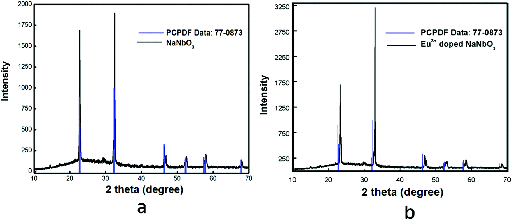
NaNbO3(s) (where ‘s’ stands for solid sample) was synthesized through a solid-state route by heating an equimolar mixture of 0.2119 g of Na2CO3(s) and 0.5316 g of Nb2O5(s) at 900 °C in a high-purity Ar atmosphere (to obtain, 99.999% pure argon gas was passed through silica gel, metallic calcium and P2O5(s) in order to remove the bulk moisture, oxygen and trace moisture, respectively) for 100 h with intermediate grinding after 20 h time interval. Before initiating the heating procedure, the starting materials were ground thoroughly for 1 h so that homogeneous mixtures were formed. The final temperature of 900 °C was reached through many heating steps and in each step the temperature was raised by 100 °C at a heating rate of 5 °C min−1. After completing the heat treatment procedure at 900 °C, the sample mixture was cooled down to room temperature in the same experimental condition at a cooling rate of 5 °C min−1. When the synthesis procedure was completed, the sample was stored in vacuum in order to avoid any contamination. Formation of the pure compound was confirmed by matching the XRD pattern with the reported one in JCPDS file No. 77-0873, as shown in Fig. 1a.
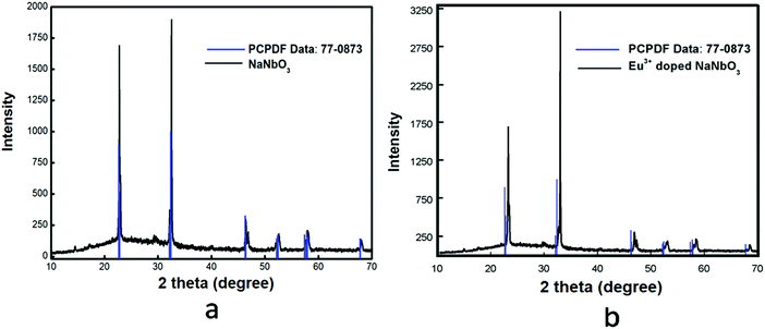 |
| | Fig. 1 Powder X-ray diffraction patterns of: (a) NaNbO3 and (b) Eu3+-doped NaNbO3. | |
Eu3+-doped NaNbO3(s)
A homogeneous and stoichiometric mixture of 0.0070 g Eu2O3(s), 0.2097 g Na2CO3(s) and 0.5316 g Nb2O5(s) was heated in order to synthesize 1.0 mol% Eu2O3(s)-doped NaNbO3(s) in a high-purity argon atmosphere at 900 °C for 100 h. A similar heat treatment process was also followed for this compound as described for pure NaNbO3(s). The purification of argon gas was also the same as mentioned before. The characterization of the sample was carried out by the X-ray diffraction technique and the spectrum is given in Fig. 1b. It can be seen from the spectrum of this Eu3+-doped NaNbO3 that there was a shift of the XRD patterns towards the higher two theta side in comparison to the undoped compound. This is only possible when Eu3+ ions are substituted at a position of a bigger cation to reduce the cell parameters; which are inversely related to the two theta value. The small impurity peaks around 2θ = 30° for both the undoped and doped compound may be due to Nb2O5.
KNbO3(s)
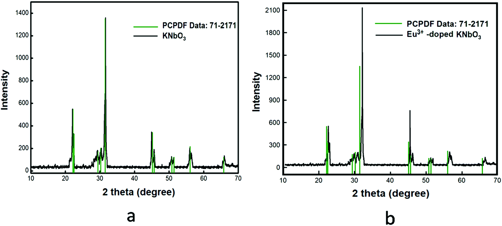
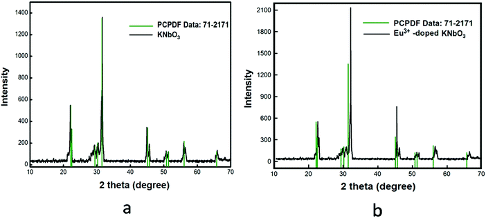
KNbO3(s) was synthesized through the solid-state route by heating a homogeneous (1![[thin space (1/6-em)]](https://www.rsc.org/images/entities/char_2009.gif) :1) mixture of 0.2764 g K2CO3(s) and 0.5316 g Nb2O5(s) at 900 °C for 100 h in a high-purity Ar gas atmosphere with heat treatment similar to that for NaNbO3. After completing the heat treatment, the sample mixture was cooled down to room temperature, like for NaNbO3, and then the sample was stored in vacuum in order to avoid any contamination. The purification process of Ar gas was the same as discussed earlier. Formation of the compound was confirmed by matching the XRD pattern with the reported one in JCPDS file No. 71-2171, as shown in Fig. 2a.
:1) mixture of 0.2764 g K2CO3(s) and 0.5316 g Nb2O5(s) at 900 °C for 100 h in a high-purity Ar gas atmosphere with heat treatment similar to that for NaNbO3. After completing the heat treatment, the sample mixture was cooled down to room temperature, like for NaNbO3, and then the sample was stored in vacuum in order to avoid any contamination. The purification process of Ar gas was the same as discussed earlier. Formation of the compound was confirmed by matching the XRD pattern with the reported one in JCPDS file No. 71-2171, as shown in Fig. 2a.
 |
| | Fig. 2 Powder X-ray diffraction patterns of: (a) KNbO3 and (b) Eu3+-doped KNbO3. | |
Eu3+ doped KNbO3(s)
1.0 mol% Eu3+-doped KNbO3(s) compound was prepared by heating a homogeneous and stoichiometric mixture of 0.0070 g Eu2O3(s), 0.2736 g K2CO3(s) and 0.5316 g Nb2O5(s) at 900 °C in a high-purity Ar environment for 100 h with the same heating conditions as described for pure KNbO3(s). The characterization of the sample was carried out using the X-ray diffraction technique and the XRD pattern is given in Fig. 2b. For this Eu3+-doped KNbO3 compound too, there was a slight shift of the XRD patterns towards a higher two theta value.
FTIR study
The FTIR spectra of undoped and Eu3+-doped niobates are presented in Fig. 3. For both the KNbO3 and NaNbO3 compounds, the absorption peaks in the range of 500–1000 cm−1 were due to the NbO6 octahedron.34,35a The band around 534 cm−1 was due to the edge-shared NbO6 octahedron, while the band around 628 cm−1 represented the O–Nb–O stretching vibration (v3 mode) in the corner-shared NbO6. A weak band around 860 cm−1 could be observed for all of the compounds, which was due to existence of a carbonate group.35b
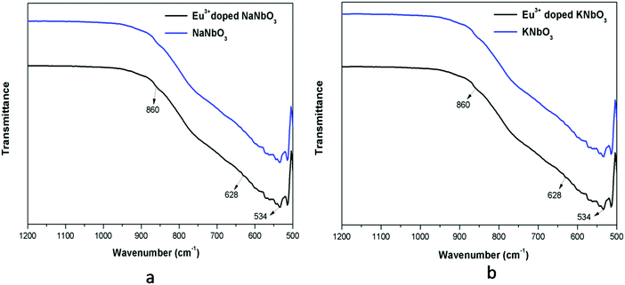 |
| | Fig. 3 FTIR spectra of: (a) undoped and Eu3+-doped NaNbO3 and that of (b) KNbO3. | |
Note: The instrumental details are given in the ESI.†
3.0. Results and discussion
3.1. Photoluminescence (PL) study
NaNbO3 and Eu3+-doped NaNbO3 (Eu3+:NaNbO3).
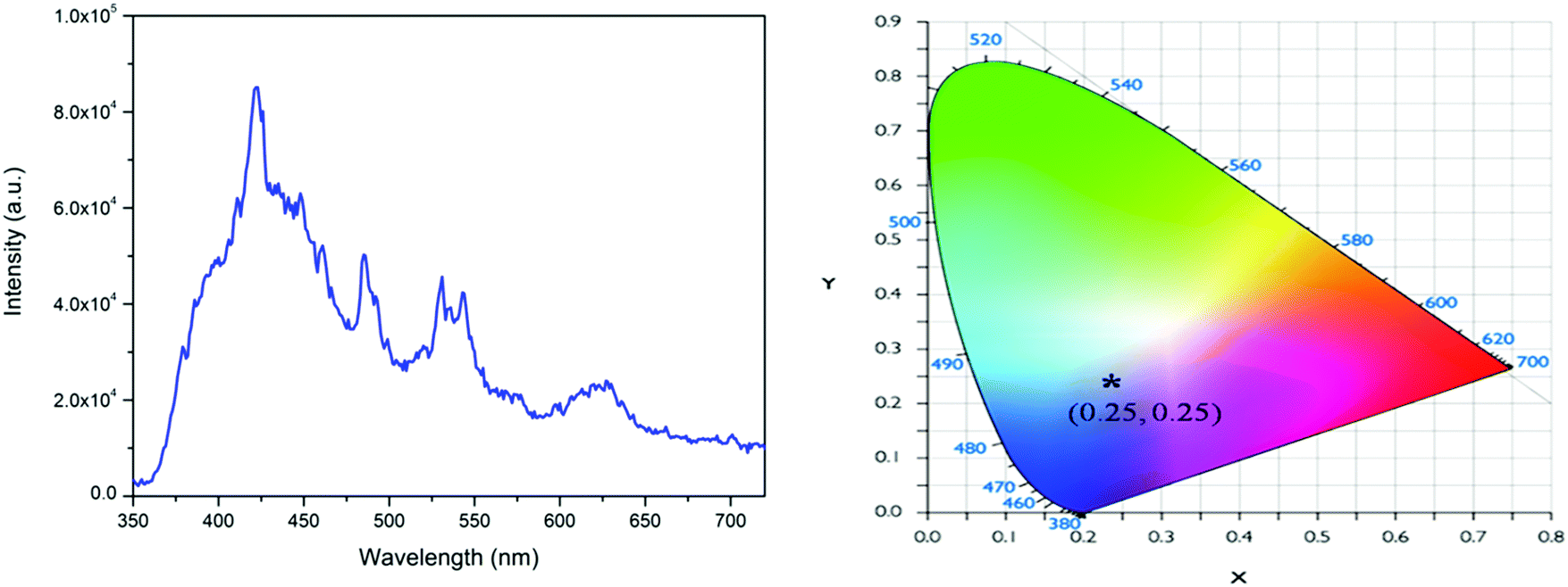
The emission spectrum of the undoped NaNbO3 compound with an excitation wavelength of 230 nm is given in Fig. 4a, which shows multiple emission bands at around 425, 480, 540 and 630 nm. Such emission bands must have originated from NbO6 octahedra12a and various defect centres, such as the different types of oxygen vacancies associated with the NbO6 octahedron, which create several trap states (shallow and deep trap states) inside the band gap of the materials, as reported earlier.12b These oxygen vacancies are mostly singly charged (VO+) or doubly charged (VO2+)12b and are associated with the NbO6 octahedron and originate due to structural order–disorder transition. The bluish 425 nm band could be attributed to NbO6 octahedron, while the bands in the green and yellow regions might be due to defect centres.12a,b The CIE colour coordinates of this compound were calculated following the earlier procedures36 and they are presented in Fig. 4b, which show that the compound was a blue-light-emitting material.
 |
| | Fig. 4 (a) Emission spectrum of NaNbO3 at 230 nm excitation and (b) its CIE colour coordinates. | |
The PL excitation spectrum of Eu3+:NaNbO3 is given in the ESI† (Fig. S1), which showed that there were multiple excitation peaks present in the 210–300 nm and 350–450 nm regions, with the peaks in the 350–450 nm range being the most intense. The excitation peaks in the 350–450 nm range could be attributed to the characteristic excitation bands of Eu3+ ion, arising due to the f–f transitions. The peaks in the 210–300 nm range were due to the charge-transfer (CT) transitions from the p orbital of oxygen to the empty d orbital of the Eu3+ ion and to the empty 4d orbital of the Nb5+ ion in the NbO6 groups.25,26 Since we aimed to investigate both host- and dopant-induced emission, the emission spectra were recorded with the charge-transfer excitation for the doped compounds. Fig. 5 shows the PL emission spectrum of Eu3+:NaNbO3 with CT excitation, which was composed of both the host's emission and the prominent characteristics transition lines of Eu3+ ions. The orange 5D0–7F1 (594 nm) and the red 5D0–7F2 (614 nm) transition lines of the Eu3+ ion, which correspond to magnetic dipole (MD) transition and electric dipole (ED) transition were clearly visible in the spectrum. In addition, the emission line at 715 nm (5D0–7F4) was also visible. The calculated colour coordinates for this compound are presented in the inset of Fig. 5, which shows that the compound was a pink-colour-emitting phosphor material. Generally, Eu3+-doped compounds are red in nature; however, in the present case, the prominent blue emission from the host in combination with the red emission from Eu3+ ions gave rise to the pink colour. It is well known that the relative intensity ratio of the ED and MD lines (i.e. ED/MD), which is also known as the asymmetric ratio (A), measures the degree of distortion from the inversion symmetry around the Eu3+ ion.25–27 Thus, the higher intensity ED line indicated that the dopant Eu3+ ion was situated at a lattice site within a highly distorted environment. This distortion occurs due to the size and charge differences of the Eu3+ ion with the two host cations, i.e. Na+ and Nb5+. The respective ionic radii were 0.94 Å for the 6-co-ordinated Eu3+, 1.12 Å for the 9-co-ordinated Eu3+ (maximum reported Shannon radius of a Eu3+ ion), 1.39 Å for the 12-coordinated Na+ and 0.64 Å for the 6-co-ordinated Nb5+ ion. Thus from an ionic radius point of view, the Eu3+ ions are more likely to replace the bigger sized Na+ ions since the size difference with the smaller Nb5+ ion is more. This was also supported by the XRD pattern of the Eu3+-doped NaNbO3 compound, which showed a shift of the pattern towards the higher two theta side and that is only possible when a smaller dopant ion replaces a bigger lattice ion. The other factor that can induce more distortion into the lattice site is the charge imbalance. Since there will be a charge difference of two at any of the two lattice sites in this matrix when a Eu3+ ion is doped, defect centres with opposite charges must have to originate as a counterbalance. Such defect centres might be close or far from the lattice sites and the distance will determine the amount of induced distortion in the lattice site. However, there is always a possibility that a few percentages of Eu3+ ions may also replace the smaller Nb5+ ions from the respective lattice site and in such a case there will be two different kinds of Eu3+ ions (one at a Na-site and another at a Nb-site). Lifetime study can provide significant information in this context, which is discussed later.
 |
| | Fig. 5 Emission spectrum of Eu3+:NaNbO3 at 250 nm excitation wavelength and its CIE colour coordinates (inset). | |
KNbO3 and Eu3+-doped KNbO3 (Eu3+:KNbO3).
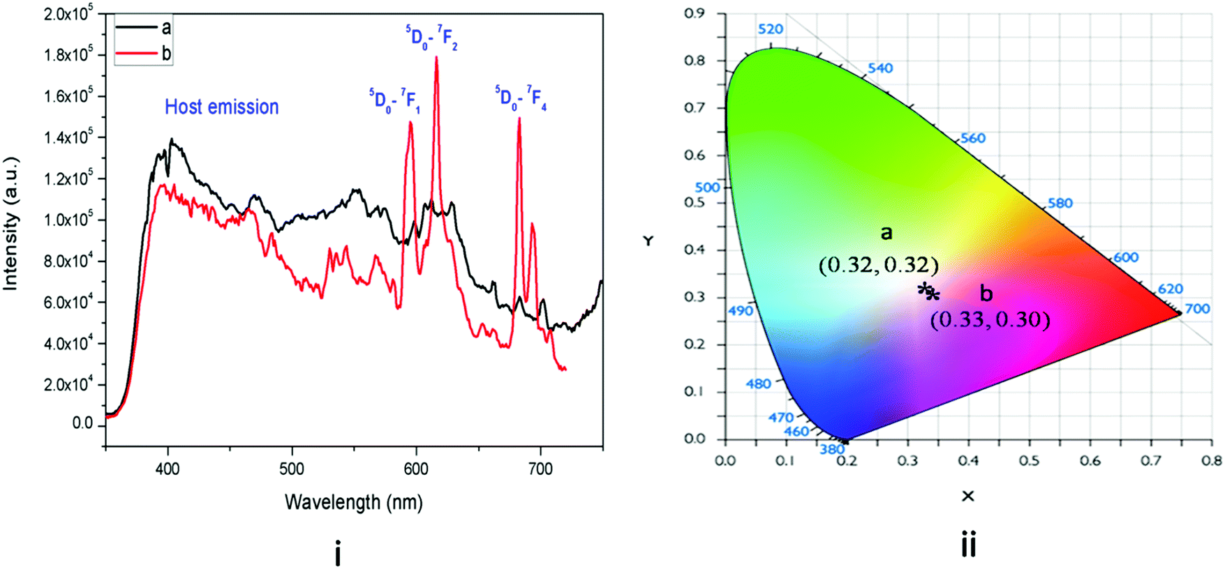
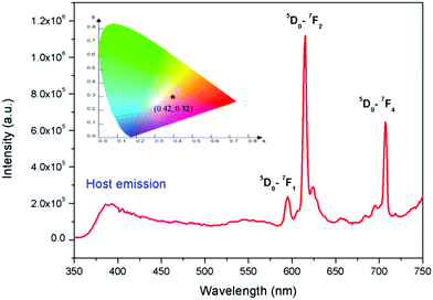
Fig. 6 presents the emission spectra of undoped KNbO3 and Eu3+:KNbO3 compounds at 250 nm excitation wavelength. The excitation spectrum of Eu3+:KNbO3 is provided in the ESI† (Fig. S2). It can be seen that for the undoped compound there was a broad emission band consisting of several emission components. Such a broad emission band must have originated from NbO6 octahedron and several defect centres associated with it, as observed in the case of NaNbO3.12 Upon doping with Eu3+ ions, in addition to the host emission, peaks due to Eu3+ ions also appear in the spectrum. Here the emission intensity arising due to the host and Eu3+ are comparable unlike that in Eu3+:NaNbO3, where the host emission was suppressed upon Eu3+ doping. One possibility is the energy transfer from the host to the dopant ion in NaNbO3, since the 395 nm excitation peak of Eu3+ matches the bluish emission of the NbO6 octahedron. However, such an energy-transfer mechanism may not exist in KNbO3, as evident from the intense host emission. Later, we discuss how the site occupancy of Eu3+ ions is different in NaNbO3 and KNbO3 and this might be one reason. In Eu3+:KNbO3, Eu3+ ions prefer to occupy Nb sites, which may create additional oxygen-vacancy-related defects. Since NbO6 octahedra connect to each other via corner sharing through the oxygen linkage, any oxygen vacancy can quench the blue emission of the NbO6 octahedron. On the other hand in NaNbO3, the Eu3+ ions prefer to occupy Na+ sites which results in two additional positive charges in the matrix. Thus the possibilities of the formation of positively charged oxygen vacancies are less and instead there will be the creation of negatively charged defects. Further, from the respective intensity of the ED and MD lines of Eu3+ ions, it can be inferred that the asymmetry ratio is less in KNbO3 compared to that in NaNbO3 and that the Eu3+ ions have a more symmetrical environment in KNbO3. We also calculated the CIE colour coordinates as shown in Fig. 6-ii, which suggested that upon doping a Eu3+ ion, the Eu3+:KNbO3 compound behaved as a white-light-emitting material. This was due to the mixing of the red emission of Eu3+ ions with the blue and green emissions from the host. Since the host showed a very prominent emission in the blue and green regions unlike in NaNbO3, the realization of white light emission was possible in the single-phase Eu3+-doped KNbO3 compound, which offers many advantages over the others.33 The host emission also behaved as a white light. It is worth mentioning here that the emission spectra of both the compounds (Eu3+:KNbO3 and Eu3+:NaNbO3) at 395 nm excitation wavelength (characteristic excitation wavelength of Eu3+ ions) were also recorded and are provided in the ESI† (Fig. S3 and S4). This was to check whether the ratio of the ED and MD lines followed a similar trend as observed with the 250 nm excitation. It was observed that the ratio of ED and MD lines followed a similar trend. Interestingly, we observed that the splitting pattern of the emission line at 715 nm (5D0–7F4) was different in Eu3+:KNbO3 and Eu3+:NaNbO3. This also suggested that the lattice site occupancy or the surrounding environment of the Eu3+ ion was different in these compounds. Now for both the doped compounds, there were multiple cationic sites wherein Eu3+ ions could get distributed. Two major factors that will determine the dopant ion's distributions are: (a) the size difference and (b) the charge differences between the dopant ions and host's cations. A PL lifetime study is the most suitable technique to obtain information about the existence of different Eu3+ environments.
 |
| | Fig. 6 (i) Emission spectra of: (a) undoped and (b) Eu3+:KNbO3 at 250 nm excitation and (ii) its CIE colour coordinates. | |
PL lifetime study.
The respective decay curves of Eu3+:NaNbO3 and Eu3+:KNbO3 are given in Fig. 7. It could be observed that both compounds followed a tri-exponential behaviour as mentioned in eqn (1)| | 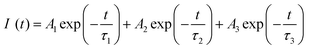 | (1) |
where I(t) is the intensity, τ1, τ2 and τ3 are the emission decay times, and A1, A2 and A3 are their relative weightings. These lifetime values with their respective magnitudes are given in Table 1.
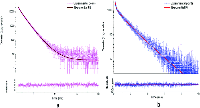 |
| | Fig. 7 Photoluminescence decay profiles of: (a) Eu3+:NaNbO3 and (b) Eu3+:KNbO3 at an excitation wavelength of 395 nm and emission wavelength of 615 nm. | |
Table 1 Photoluminescence lifetime values of the Eu3+-doped niobate compounds
| Compound |
τ
1 in millisecond |
τ
2 in millisecond |
τ
3 in millisecond |
| Eu3+:NaNbO3 |
0.33 (6%) |
0.96 (80%) |
1.69 (14%) |
| Eu3+:KNbO3 |
0.07 (4%) |
0.62 (25%) |
1.38 (71%) |
From Table 1, it can be seen that three different emitting components existed for the Eu3+:NaNbO3 compound and the 2nd lifetime component (0.96 ms) with the intermediate lifetime value had the highest contribution. On the contrary, in the case of Eu3+:KNbO3, the long-lived component (1.38 ms) had the highest contribution among the three components. Since f–f transitions of Eu3+ ions are forbidden in nature and only in an asymmetric environment do they become partially allowed, the short lifetime value must be associated with a distorted or asymmetric environment of Eu3+ ions, while the long-lived component may be associated with a more symmetric environment.25,26 Thus for Eu3+:NaNbO3, the τ3 = 1.69 ms is attributed to Eu3+ ions in a more symmetrical environment while τ2 = 0.96 ms is attributed to Eu3+ ions in an asymmetrical environment. In ABO3 type of perovskite, the B-atom resides in a symmetrical octahedron, i.e. BO6. On the other hand, the A-atom with twelve co-ordinations has a relatively more asymmetrical environment. Further, since this site is created by the corner sharing of oxygen atoms from the surrounding 8 BO6 octahedra, which are very often tilted due to the slight mismatch of the ionic radii of A and B atoms, the 12 oxygen atoms are not symmetrically co-ordinated towards the A atom. Therefore we may attribute the long-lived lifetime (τ3 = 1.69 ms) component to the Eu3+ ion at the Nb site, while the other component with a lower lifetime value (τ2 = 0.96 ms) may be attributed to Eu3+ ion at the asymmetric Na site. The τ1 = 0.33 ms lifetime component, which makes the very least contribution among the three, might be due to Eu3+ ion present in a highly asymmetric environment or close to an impurity or defect centre that acts as a quencher. In the FTIR spectra, we could observe the presence of small carbonate impurity, which may quench the excited state. However, since the contribution is very much less, we believe that such a Eu3+ ion will not have any significant impact on the physical properties of the materials. The fact that the percentage of the τ2 = 0.96 ms component is more in the Eu3+:NaNbO3 compound indicates that most of the Eu3+ ions are placed in a distorted environment. From the emission spectra too, it is clear that the intensity of the ED line is very high compared to the MD line, resulting in an asymmetric ratio of A > 1.
On the contrary in the Eu3+:KNbO3 compound, the contribution from the long-lived component (τ2 = 1.38 ms) is more than from the short-lived components (τ1 = 0.07 ms & τ2 = 0.61 ms), which suggests that most of the Eu3+ ions exist in a symmetrical environment, here at Nb sites. Considering the respective ionic radii of K+ (rK+ = 1.64 Å) and Eu3+ ions (rEu3+ = 1.12 Å for 9 co-ordination), it is more likely that Eu3+ ions do not prefer to replace a much bigger ion like K+ unlike the Na+ ion in Eu3+:KNbO3. The fact that the lifetime value of the long-lived component (τ2 = 1.38 ms) is less compared to that in Eu3+:KNbO3 can be explained on the basis of oxygen vacancies associated with the NbO6 octahedron. If Eu3+ ions replace Nb5+ ions, oxygen vacancies will be created, which can quench the excited state. The τ2 = 0.62 ms component might be due to Eu3+ ions close to an impurity centre, like a carbonate. Another possibility is that the long-lived component is due to Eu3+ ions placed at Nb sites with a fewer defect centres, while the short-lived component is due to Eu3+ ions at similar sites but with a higher number of defect centres. We believe that the τ1 = 0.07 ms is not due to the Eu3+ ions as it rarely shows a lifetime value in this order due to forbidden nature of the f–f transition. Rather, it will be some defect related component, and here, in KNbO3, it can be seen that the host has an emission band around 600 nm. The fact that the defect centres play an important role in the lifetime value of the Eu3+ ions is also reflected in the lower intensity of the Eu3+ ion's characteristic lines (ED & MD) in Eu3+:KNbO3 compared to that in Eu3+:NaNbO3. The few defect centres in the Eu3+:KNbO3 compound may quench the excited state via a nonradiative pathway, thereby reducing both the lifetime and intensity from Eu3+ ions. Now if we critically view the emission profile, then it can be concluded that the intensity ratio, i.e. the ED/MD, or the asymmetric ratio is very low compared to that in the Eu3+:NaNbO3 compound. However, due to the significant contribution from the host emission, it is difficult to get a clear picture about the characteristics of the emission lines. The best way is to isolate the individual spectra by giving different delay times once all of them are excited in the TRES study. In this way, we found that the lifetime values of the host emission at 400, 440, 470 and 550 nm were 11.22, 10.78, 10.87 and 11.03 μs, respectively, which were less than that of the Eu3+ ion. The decay profiles of these emission wavelengths are given in the ESI† (Fig. S5–S8). Therefore, a systematic TRES study at different delay times can provide a clearer picture about the host emission as well as the emission from Eu3+ ions.
Time-resolved emission spectroscopy (TRES) study of Eu3+:KNbO3.
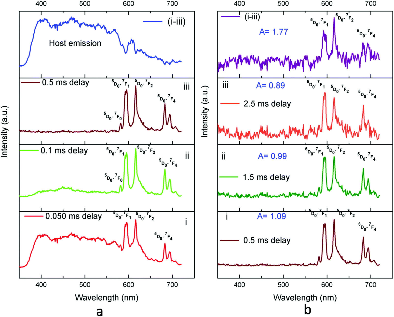
TRES analysis of the Eu3+:KNbO3 compound was carried out following similar procedures as demonstrated in our earlier work.37 The TRES spectra at different delay times are given in Fig. 8. It can be seen that with increasing the delay time, the spectral features are changed gradually. At a smaller delay time, such as at 0.050 ms, the spectrum is composed of both the host emission as well as the emission from Eu3+ ions. However, as we kept on increasing the delay time, the host emission started disappearing. This was due to the lower lifetime value of the host emission. At 0.5 ms delay time, the host emission had completely disappeared, and if we properly subtract it from the TRES spectrum at 0.050 ms delay time, a clear picture of the host emission profile can be obtained, as given in the top of Fig. 8a. Now at 0.5 ms delay time, the spectral features of the Eu3+ ion is clearly visible and the ED and MD lines are almost equally intense, with ED being slightly higher intense. However, as we further increased the delay time, a complete different picture was observed, and at higher delay time such as at 2.5 ms delay, the MD line was found to be more intense with an asymmetric ratio of <1. This was due to the fact that at this time delay the spectrum was only composed of the long-lived Eu3+ component with a lifetime value of 1.39 ms. This Eu3+ ion occupied a symmetrical lattice site and thus the MD line was more intense. The emission spectrum of the Eu3+ ion existing in an asymmetric site can be obtained if we subtract the TRES spectrum at 2.5 ms from that at 0.5 ms. At 0.5 ms delay time, the emission spectrum was composed of both the short-lived and long-lived components and at 2.5 ms delay time (which is more than three times the lifetime value of the short-lived component), the short-lived component must have been decayed completely. The emission spectrum of the short-lived component is given at the top of Fig. 8b, which had an asymmetry ratio of A = 1.77. While for the long-lived component in Fig. 8b-iii, it is clearly visible that A < 1 owing to the less intense ED line. Therefore, from these observations in the lifetime and TRES studies, it was confirmed that the local structure around the Eu3+ ion in Eu3+:KNbO3 was more symmetric in nature compared to that in Eu3+:NaNbO3, where it was asymmetric. We further confirmed this observation later by EXAFS study.
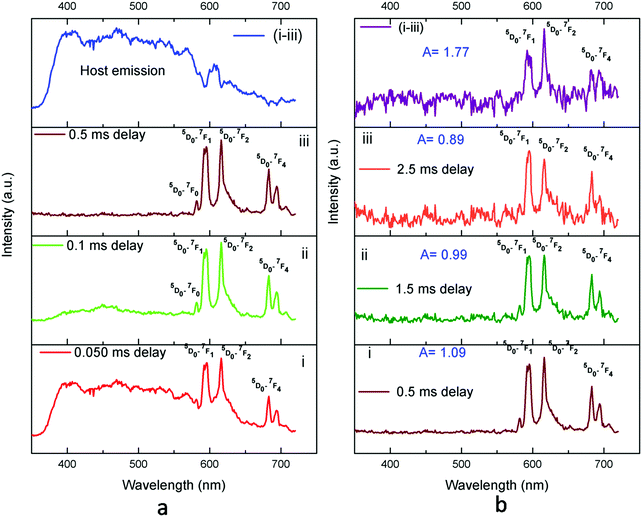 |
| | Fig. 8 TRES spectra of Eu3+:KNbO3 at different delay times. | |
Another way to understand the local distortion is to understand the site symmetry from the Stark splitting pattern of the characteristics lines of Eu3+ ions as described elsewhere.38 However, to understand such symmetry, the splitting patterns must be clearly visible. From the emission spectra of the Eu3+ ions, we saw that the 5D0–7F0 line existed for both the compounds but with a higher intensity for the Eu3+:KNbO3 compound. The existence of a 5D0–7F0 line indicated that Eu3+ existed at a low-symmetry site without an inversion centre. The 5D0–7F0 line is only allowed with the 10 site symmetries, i.e. Cs, C1, C2, C3, C4, C6, C2V, C3V, C4V and C6V respectively.38 From the Stark splitting pattern (Fig. S9, which is given in the ESI†), we observed that the site symmetry of Eu3+ ion in NaNbO3 might be C4V. Although, the 5D0–7F0 line was clearly visible in the emission spectrum of Eu3+ ions in KNbO3, the splitting of other peaks was not clear to us and hence we did not calculate the site symmetry for the case of KNbO3. However, the symmetry must be among the 10 mentioned symmetries. This also suggested that although the MD line had good intensity in Eu3+:KNbO3, the Nb site was not purely symmetric in nature, i.e. it was a site with inversion symmetry. This might be due to the fact that the defect centres, such as oxygen vacancies, created some asymmetric environment surrounding the Nb site as stated earlier. Now, let us see what happened to the electrical properties of KNbO3 and NaNbO3 when Eu3+ ion was doped, which was another important physical property investigated in this present work.
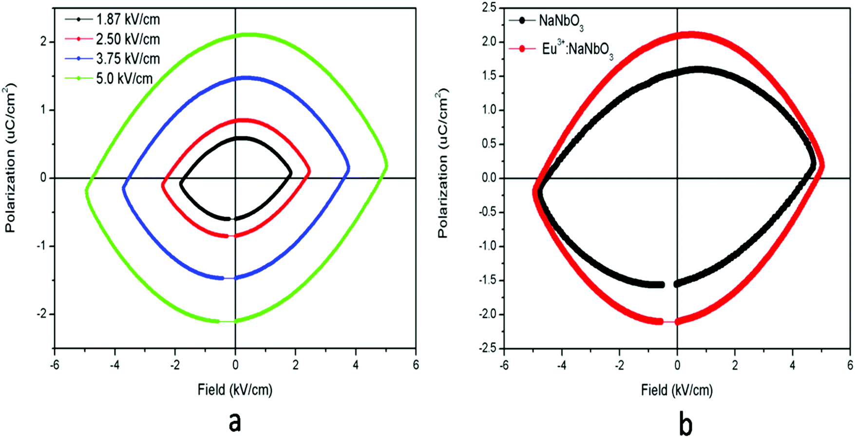
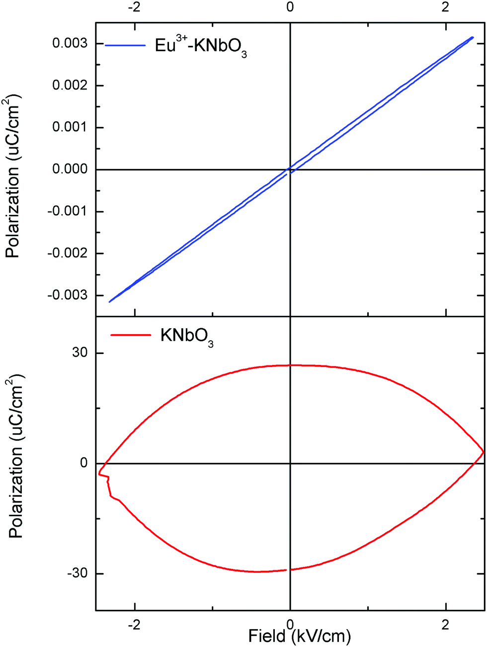
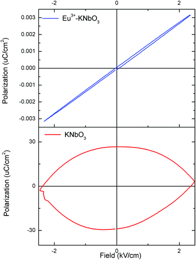
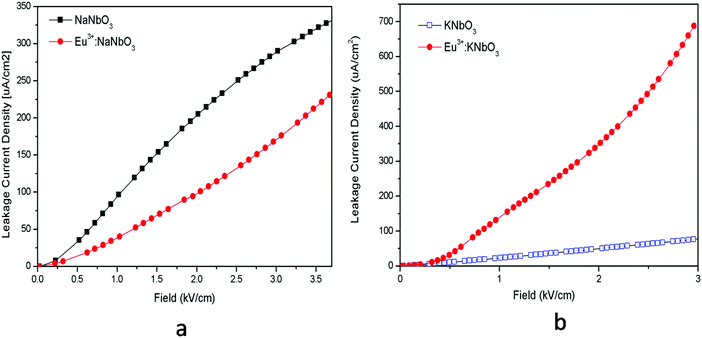
3.2. Electrical properties
The ferroelectric (P–E) hysteresis loops of the Eu3+:NaNbO3 compound at room temperature and at different electrical fields are shown in Fig. 9a, wherein it is clearly visible that the polarisation is at a maximum at a field of 5 kV cm−1. A similar observation was also found for the NaNbO3 samples. The compound showed saturation in polarization and also a concave region in the P–E plot, which suggested that it is truly ferroelectric in nature.39 The ferroelectric (P–E) hysteresis loops for undoped NaNbO3 and Eu3+:NaNbO3 compounds at a field of 5 kV cm−1 are shown in Fig. 9b. From the plot, we measured the respective remnant polarization of both these samples and they were Pr = 1.65 μC cm−2 for NaNbO3 and Pr = 2.16 μC cm−2 for Eu3+:NaNbO3. Thus, there was an enhancement of the polarization value when Eu3+ ions were doped. Interestingly, the KNbO3 series of compounds showed a reverse trend and the ferroelectric (P–E) hysteresis loops of Eu3+:KNbO3 and KNbO3 are presented in Fig. 10. Here, although the undoped KNbO3 compound showed a ferroelectric hysteresis loop; upon doping with Eu3+ ions, the compound showed very weak ferroelectric behaviour. We also measured the leakage current density of these compounds. The leakage current density vs electric field plot for NaNbO3 and KNbO3 compounds are presented in Fig. 11, which suggests that the leakage current was less in the case of the Eu3+:NaNbO3 compound at any point of the field compared to the undoped NaNbO3 compound. On the other hand, in the KNbO3 series of compounds, the leakage current density was found to increase when a Eu3+ ion was doped. Thus, there must be two different factors that are responsible for such behaviour. Earlier reports on the crystal structure of NaNbO3 suggested that, due to the octahedral tilting of the perovskites, which is very common in this class of compounds and an intrinsic property of perovskites, the Nb5+ cations have some positional disorder and they lie significantly off-centre from the centrosymmetric positions towards an edge of the octahedron in a polar manner, in the “P21ma” polymorph.20 Such an off-centre position of the Nb5+ cations is mainly responsible for the polar character of the compound. Now, doping an impurity ion, such as Eu3+ ion, with a different size must increase the positional disorder due to change in the tilting of the octahedron. In NaNbO3, the respective ionic radii of the Na+, Nb5+ and Eu3+ ions were in the order rNb5+ = 0.64 Å (6 co-ordinated) < rEu3+ = 0.94 Å (6 co-ordinated) and 1.12 Å (9 co-ordinated) < rNa+ = 1.39 Å (12 co-ordinated). However in KNbO3, the respective ionic radii of K+, Nb5+ and Eu3+ ions were in the order rNb5+ = 0.64 Å (6 co-ordinated) < rEu3+ = 0.94 Å (6 co-ordinated) and 1.12 Å (9 co-ordinated) < rK+ = 1.64 Å (12 co-ordinated). Thus the substitution of Eu3+ at K+ sites may lead to the shrinkage of the KNbO3 lattice. On the other hand, the substitution at the Nb5+ site (B site) will definitely expand the unit cell volume. A study on the changes of the lattice parameters due to the substitution of lanthanides, such as Er3+, at the lattice sites of KNbO3 was reported earlier using XRD and it was concluded that Er3+ may go to both K and Nb sites.40 In our present cases too, we observed a shift in the XRD patterns towards a higher two theta side in NaNbO3 and since two theta is inversely related to the lattice parameters, it can be assumed that the majority of the Eu3+ dopant ions are substituting for the larger sized Na+ ions. However, the shift was less in the case of KNbO3 and, as discussed earlier, the major portion of the Eu3+ ions had the possibility to go to the Nb5+ site as observed in the PL lifetime study. Generally XRD does not give accurate information at the atomic scale unlike PL and EXAFS studies, which are very useful to extract such information. From the PL lifetime and TRES study, we already concluded that in KNbO3, the majority of Eu3+ ions prefer to go to the Nb site, while in NaNbO3, they have a preference for the Na site. Now as far as the ferroelectric property is concerned, substitution at only Na or K sites may have a direct impact on the ferroelectric property, since the off-centring of Nb5+ cations from the centrosymmetric positions in the NbO6 octahedron is the main reason for such a property and the substitution at Na or K sites may alter the off-centre position of Nb5+ cations. Therefore, the substitution of Eu3+ ions at Na sites might be the reason for the enhanced remnant polarization in NaNbO3, since such substitution may help to increase the off-centring parameter. The fact that substitution at the Na site in NaNbO3 may induce more disorder was also supported by an earlier EXAFS study.32 On the other hand in KNbO3, since most of the Eu3+ ions go to comparatively more symmetric Nb sites, such off-centring might be reduced, and might thereby reduce the remnant polarization. Let us now try to explain the increase in ferroelectric properties by Goldschmidt's tolerance factor ‘t’, which is defined as t = RA–O/√2 (RB–O), where RA–O and RB–O are A–O and B–O bond lengths in ABO3 perovskite. As per various studies, tilting of the BO6 octahedron in ABO3-type perovskites appears when t is below 1, while tilts do not exist when t ≥ 1.41 The t values for NaNbO3 and KNbO3 were 0.96 and 1.06, respectively.42 In NaNbO3, the tilting of NbO6 octahedra occurs due to the relatively small size of Na atoms (rNa+ = 1.39 Å), which are placed in the 12-fold-coordinated cavities between the BO6 octahedra. On the other hand in KNbO3, due to the larger size of K cations (rK+ = 1.64 Å), they fit well inside the cavities and the tilting of the NbO6 octahedron is not present. This was also reflected in the higher intensity of the MD line of Eu3+ ions in KNbO3, suggesting a more ordered structure compared to NaNbO3. Therefore, the observed ferroelectric property of KNbO3 was purely due to the inherent off-centre of Nb5+ from the centrosymmetric positions and tilting played no role in further increasing such an off-centre position of Nb5+ ions, like in NaNbO3. In NaNbO3, as smaller sized Eu3+ ions are doped at the Na site, the t values might be further reduced from the value of 0.96 and this increases the tilting of NbO6 octahedra, which makes the Nb5+ ions more off-centred from the centrosymmetric positions. On the contrary in KNbO3, the larger sized Eu3+ ions may be preferably placed at Nb5+ sites, since the size difference with K+ ions is more here. These larger size Eu3+ ions in the place of smaller sized Nb5+ ions may reduce the off-centring of Nb5+ ions in the nearby NbO6. To get more evidence we carried out an EXAFS study.
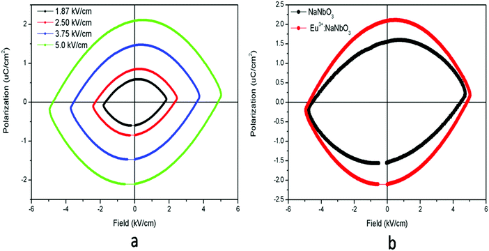 |
| | Fig. 9 Ferroelectric (P–E) hysteresis loops for: (a) Eu3+:NaNbO3 at room temperature under different electrical fields, and (b) for undoped NaNbO3 and the Eu3+:NaNbO3 compound at a field of 5 kV cm−1. | |
 |
| | Fig. 10 Ferroelectric (P–E) hysteresis loops for undoped KNbO3 and the Eu3+:KNbO3 compound at a field of 5 kV cm−1. | |
 |
| | Fig. 11 Leakage current density vs. field for: (a) NaNbO3 and Eu3+:NaNbO3 compounds and for (b) KNbO3 and Eu3+:KNbO3 compounds. | |
The leakage current density can be explained based on defect centres. It could be observed that for both the Eu3+:NaNbO3 and Eu3+:KNbO3 compounds, there was a prominent host emission band along with the Eu3+ ion's emission. These host emission bands were created due to the presence of several oxygen vacancies or defect centres, which may create many shallow or deep trap states inside the band gap as reported earlier.12 It was also observed that the host emission peaks maxima were mostly comparable to that of the Eu3+ ion's emission in Eu3+:KNbO3; while in Eu3+:NaNbO3, although the host's emission bands were clearly visible, their intensity was less compared to the Eu3+ ion's emission. This indicates that there are more defect centres being created due to Eu3+ doping in KNbO3 compared to that in NaNbO3. Now it is worth mentioning here that these defect centres might be due to the oxygen vacancies,12 which can be created only when a Eu3+ ion substitutes at a Nb5+ site. These defects may increase the ionic conductivity, which causes a higher leakage current density. Therefore, from both saturation polarisation and leakage current density observation, it could be concluded that while Eu3+ doping may enhance the NaNbO3 compound's performance for application in storage devices, the same doping may reduce such performance for the KNbO3 compound.
3.3. X-ray absorption spectroscopy studies of undoped and Eu3+:NaNbO3 and Eu3+:KNbO3 compounds
Extended X-ray absorption fine structure (EXAFS) techniques were performed on Eu3+:KNbO3 and Eu3+:NaNbO3 samples at the Nb K-edge and Eu L3 edge to probe the local structure. The measurements were carried out at the Energy-Scanning EXAFS beamline (BL-9) at the Indus-2 Synchrotron Source (2.5 GeV, 200 mA) at Raja Ramanna Centre for Advanced Technology (RRCAT), Indore, India.43,44 This beamline operates in the energy range of 4 KeV to 25 KeV. The beamline optics consists of a Rh/Pt coated collimating meridional cylindrical mirror and the collimated beam reflected by the mirror is monochromatized by a Si(111) (2d = 6.2709 Å)-based double-crystal monochromator (DCM). The second crystal of DCM is a sagittal cylinder used for horizontal focusing, while a Rh/Pt coated bendable post mirror facing down is used for vertical focusing of the beam at the sample position. Rejection of the higher harmonics content in the X-ray beam was performed by detuning the second crystal of DCM. In the case of the Nb K edge, XAS measurements were performed in transmission mode and for the Eu L3 edge, the measurements were done in fluorescence mode.
The local structure around the absorbing atom was obtained from the quantitative analysis of the EXAFS spectra. The EXAFS spectrum was obtained from the absorption spectrum using the following method. In order to take care of the oscillations in the absorption spectrum, μ(E) was converted to the absorption function χ(E), defined as follows:45
| |  | (2) |
where,
E0 is the absorption edge energy,
μ0(
E0) is the bare atom background and Δ
μ0(
E0) is the step in
μ(
E) value at the absorption edge. The energy-dependent absorption coefficient
χ(
E) was converted to the wave-number-dependent absorption coefficient
χ(
k) using the relation,
| |  | (3) |
where,
m is the electron mass.
χ(
k) is weighted by
k2 to amplify the oscillation at high
k and the
χ(
k)
k2 functions are Fourier transformed in
R space to generate the
χ(
R)
versus R spectra in terms of the real distances from the centre of the absorbing atom. The set of EXAFS data analysis programmes available within the Demeter software package were used for the EXAFS data analysis.
46 This included background reduction and Fourier transform to derive the
χ(
R)
versus R spectra from the absorption spectra (using ATHENA software), generation of the theoretical EXAFS spectra starting from an assumed crystallographic structure and finally fitting of the experimental data with the theoretical spectra using ARTEMIS software.
Eu3+:NaNbO3.
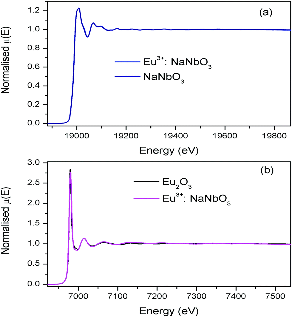
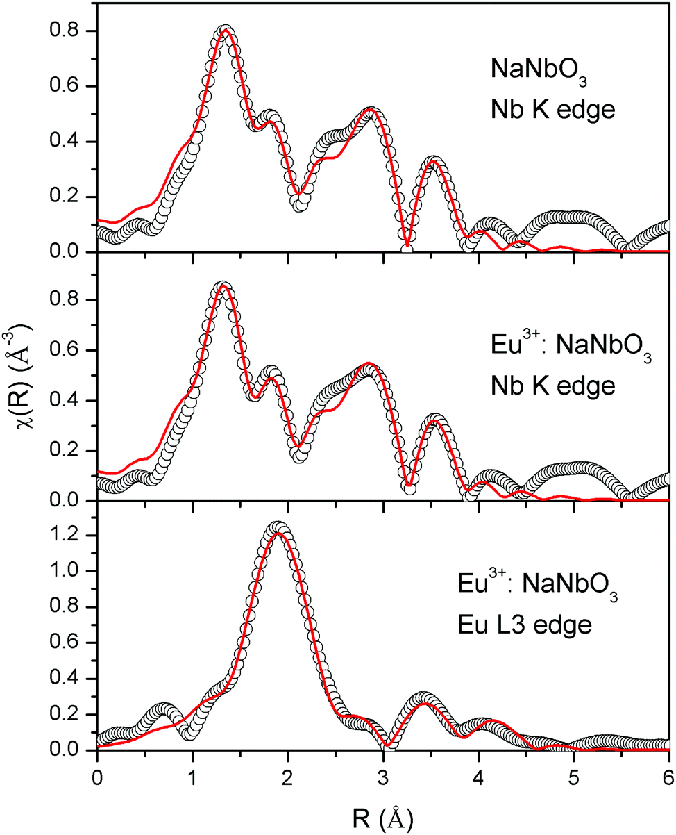
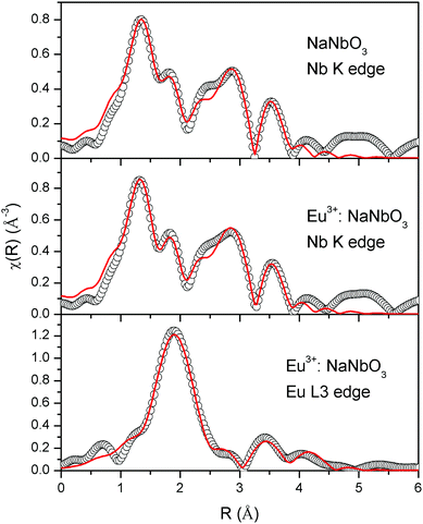
The normalised absorption spectra at the Nb K edge and Eu L3 edge are shown in Fig. 12 for NaNbO3 and Eu3+:NaNbO3. The χ(R) versus R plots were generated using Fourier transform from the μ(E) versus E spectra following the methodology as described above and are shown in Fig. 13, which shows the phase-uncorrected spectra, where the coordination peak in the Fourier transform spectra appeared at a slightly lower R compared to the actual bond length. For quantitative information, experimental χ(R) versus R plots were fitted with theoretical plots, generated using the structural parameters (atomic coordination and lattice parameters) of NaNbO3 obtained from the ICSD data base.47,48 The bond length and disorder factor (σ2) were the fitting parameters obtained during the above analysis. The fitting results are shown in Table 2 and the fitted spectra are plotted in Fig. 13. The doublet peak between 1 Å and 2 Å was a contribution of three oxygen coordination distances at 1.86, 1.93 and 2.12 Å, respectively. The second doublet peak between 2–3.25 Å was contribution of Nb–Na coordination at a distance of 3.39 Å. The third coordination peak at 3.5 Å was contribution of Nb–Nb, Nb–O and multiple scattering paths. Similarly, the Nb coordination behaviour was also obtained for Eu3+:NaNbO3 (middle panel). The Fourier transform EXAFS spectrum of the Eu L3 edge is shown in Fig. 13 (lower panel). The first coordination peak is a contribution of two oxygen coordination shells at 2.32 and 2.46 Å. This Eu–O bond distance was larger than the Nb–O bond length. This was expected due to the relatively larger ionic radius of Eu3+. The second peak at 3.5 Å was a contribution of Eu–Na and Eu–Nb coordination with a large distortion (larger σ2).
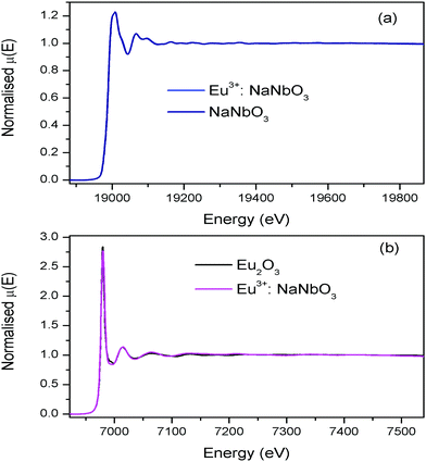 |
| | Fig. 12 (a) Nb K-edge normalised absorption spectra of NaNbO3 and Eu3+:NaNbO3; (b) Eu L3 edge normalised absorption spectra of Eu2O3 and Eu3+:NaNbO3. | |
 |
| | Fig. 13 Fourier transformed EXAFS spectra of NaNbO3 and Eu3+:NaNbO3. The experimental spectra are represented by scatter points and the theoretical fit is represented by the solid line. | |
Table 2 Bond lengths, coordination numbers and disorder factors obtained by EXAFS fitting at the Nb K-edge and Eu L3 edge of Eu3+:NaNbO3
| NaNbO3 Nb edge |
Eu3+:NaNbO3 Nb edge |
Eu3+:NaNbO3 Eu edge |
| Path |
R (Å) |
N
|
σ
2
|
R (Å) |
N
|
σ
2
|
Path |
R (Å) |
N
|
σ
2
|
| Nb–O |
1.86 |
2 |
0.0152 |
1.86 |
2 |
0.0151 |
Eu–O |
2.32 |
2 |
0.0011 |
| Nb–O |
1.93 |
2 |
0.0024 |
1.91 |
2 |
0.0027 |
Eu–O |
2.46 |
4 |
0.0053 |
| Nb–O |
2.12 |
2 |
0.0024 |
2.12 |
2 |
0.0027 |
Eu–Na |
3.66 |
3 |
0.0151 |
| Nb–Na |
3.39 |
5 |
0.010 |
3.37 |
5 |
0.010 |
Eu–Nb |
4.31 |
6 |
0.0188 |
| Nb–Nb |
3.82 |
6 |
0.0256 |
3.81 |
6 |
0.0254 |
|
|
|
|
| Nb–O |
4.14 |
6 |
0.0135 |
4.12 |
6 |
0.0112 |
|
|
|
|
Eu3+:KNbO3.
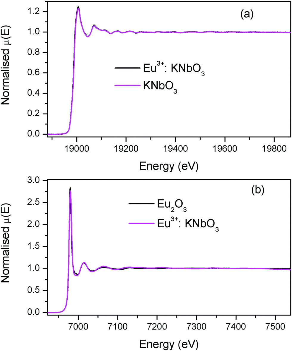
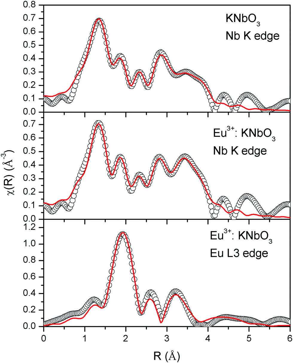
The normalised absorption spectra at the Nb K edge and Eu L3 edge are shown in Fig. 14 for KNbO3 and Eu3+:KNbO3 compounds. The χ(R) versus R plots generated using Fourier transform from the μ(E) versus E spectra following the methodology as described above are shown in Fig. 15, which shows the phase-uncorrected spectra, where the coordination peak in the Fourier transform spectra appeared at a slightly lower R compared to the actual bond length. For quantitative information, experimental χ(R) versus R plots were fitted with theoretical plots generated using the structural parameters (atomic coordination and lattice parameters) of KNbO3 obtained from the ICSD data base.49 The fitting results are shown in Table 3 and the fitted spectra are plotted in Fig. 15. The Fourier transform EXAFS spectra of KNbO3 showed a multiple number of coordination peaks. The first doublet peak between 1 and 2 Å was due to a contribution of three oxygen coordination at the distances of 1.87, 2.04 and 2.08 Å. The triplet peak between 3.5 and 4.25 Å was due to a contribution of Nb–K, Nb–Nb and multiple scattering paths. The coordination peaks were similar for Eu3+:KNbO3. The Fourier transform EXAFS spectra at the Eu L3 edge is shown in Fig. 15 (lower panel). The first peak at 2.0 Å is a contribution of two Eu–O coordination at 2.45 and 2.71 Å. The second and third peaks were fitted with Eu–K and Eu–Nb coordination at 3.82 and 4.57 Å, respectively. The obtained Eu–O bond length was relatively larger than the Nb–O bond length due to the larger ionic radius of the Eu3+ ion.
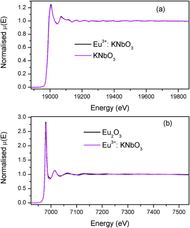 |
| | Fig. 14 (a) Nb K-edge normalised absorption spectra of KNbO3 and Eu3+:KNbO3; (b) Eu L3 edge normalised absorption spectra of Eu2O3 and Eu3+:KNbO3. | |
 |
| | Fig. 15 Fourier transformed EXAFS spectra of KNbO3 and Eu3+:KNbO3 compounds. The experimental spectra are represented by scatter points and the theoretical fitting is represented by the solid line. | |
Table 3 Bond lengths, coordination numbers and disorder factors obtained by EXAFS fitting at the Nb K-edge and Eu L3 edge of Eu3+:KNbO3
| KNbO3 Nb edge |
Eu3+:KNbO3Nb edge |
Eu3+:KNbO3Eu edge |
| Path |
R (Å) |
N
|
σ
2
|
R (Å) |
N
|
σ
2
|
Path |
R (Å) |
N
|
σ
2
|
| Nb–O |
1.87 |
2 |
0.0030 |
1.88 |
2 |
0.0012 |
Eu–O |
2.45 |
4 |
0.0017 |
| Nb–O |
2.04 |
2 |
0.0142 |
2.04 |
2 |
0.0015 |
Eu–O |
2.71 |
2 |
0.0010 |
| Nb–O |
2.08 |
2 |
0.0091 |
2.09 |
2 |
0.0045 |
Eu–K |
3.82 |
6 |
0.0185 |
| Nb–K |
3.60 |
6 |
0.0017 |
3.62 |
6 |
0.011 |
Eu–Nb |
4.57 |
6 |
0.0201 |
| Nb–Nb |
3.83 |
6 |
0.0010 |
3.89 |
6 |
0.0010 |
|
|
|
|
| Nb–O |
4.43 |
4 |
0.0089 |
4.40 |
4 |
0.0087 |
|
|
|
|
From the observed parameters from the EXAFS study as included in Tables 2 and 3, it can be seen that the distortion parameter σ2 for the Nb–O bonds were greater for the NaNbO3 compounds than the KNbO3 compounds, which supports the higher polar character of the NaNbO3 compounds compared to the KNbO3 compounds. Further in NaNbO3, upon Eu3+ doping, the σ2 value for some of the Nb–O bonds was found to increase slightly. This confirmed that Eu3+ ions induced more distortion in NaNbO3, leading to a higher polar character. On the contrary in KNbO3, upon Eu3+ doping, the σ2 value for some of the Nb–O bonds was found to decrease significantly. This suggests that the compounds became less distorted. Thus, the EXAFS results strongly support our conclusion that it is the preference of site occupancy of the Eu3+ dopant ion that changes the local distortion in these compounds, thereby controlling their electrical properties.
4.0 Conclusion
Undoped and Eu3+-doped NaNbO3 and KNbO3 compounds were synthesised through a solid-state method followed by their characterisation using XRD, FTIR, PL, electrical and EXAFS studies. The PL study revealed that the Eu3+:NaNbO3 compound was a pink-colour-emitting phosphor, where the bluish emission from the host in combination with the red emission from the Eu3+ ion gave rise to the pink colour. On the contrary, the Eu3+:KNbO3 compound was a white-light-emitting material and such a single-phase white-light-emitting material has several advantages over the others. Host emission in this compound is very prominent and superimposed with the Eu3+ ion's emission, making it difficult to analyse the characteristics peaks of the Eu3+ ion. However, with the help of TRES study, it was possible to isolate both the host and Eu3+ ion's emission and a clear picture about the transition lines of the Eu3+ ions were observed. From the respective transition lines (ED and MD) and their variation in NaNbO3 and KNbO3 compounds, it was observed that the asymmetric character surrounding the Eu3+ ion was greater in NaNbO3, while it was less in KNbO3. Further, from the PL lifetime study, it was observed that multiple Eu3+ components existed in both the compounds. However, the distribution of Eu3+ ions was greater in the asymmetric environment in the NaNbO3 compound, while in case of KNbO3, they preferably went into the symmetric environment. We concluded that in NaNbO3, most of the Eu3+ ions go to the Na lattice site, while in KNbO3, they go to the K site. Electrical study of these compounds showed that they were ferroelectric in nature and the Eu3+ doping had a huge impact on the remnant polarization. In the Eu3+-doped NaNbO3 compound, the polarization value was found to increase upon Eu3+-ion doping. However, for the KNbO3 compound, there was a drastic decrease in the remnant polarization from the undoped compound. Tilting of the NbO6 octahedron, which arose due to the mismatch of the size of A and B cations in ABO3-type perovskites made the Nb5+ cation relatively off-centre from the centrosymmetric position in the NbO6 octahedron and responsible for such ferroelectric behaviour. More, the distortion in NbO6 octahedron impacted more the polarisation characteristics. From EXAFS study, it was observed that the distortion parameter σ2 for the Nb–O bonds of the NbO6 octahedron in NaNbO3 compounds was increased when Eu3+ ions were doped. On the contrary, the same was decreased in KNbO3. Thus, we concluded that the Eu3+ ion's substitution at the Na site induced more distortion in nearby NbO6 octahedra and was responsible for the increase in remnant polarization. On the contrary, in KNbO3, Eu3+-ion substitution at the Nb site basically reduced the distortion in nearby NbO6 octahedra compared to that in the undoped compound and thus led to a decrease in polarization.
Conflicts of interest
All the authors hereby declare that they have no conflicts of interest.
Acknowledgements
The authors thank Dr Bal Govind Vats FCD, BARC for the FTIR measurements. The work is fully funded by BARC. No external funding agency is involved.
References
- X. Chen, J. Fang, X. Zhang, Y. Zhao and M. Gu, ACS Photonics, 2017, 4(9), 2102 Search PubMed.
- C. Simão, M. Mas-Torrent, N. Crivillers, V. Lloveras, J. M. Artés, P. Gorostiza, J. Veciana and C. Rovira, Nat. Chem., 2011, 3, 359 Search PubMed.
- A. Canales, X. Jia, U. P. Froriep, R. A. Koppes, C. M. Tringides, J. Selvidge, C. Lu, C. Hou, L. Wei, Y. Fink and P. Anikeeva, Nat. Biotechnol., 2015, 33, 277 Search PubMed.
- H.-Y. Li, H. Xu, S.-Q. Zang and T. C. W. Mak, Chem. Commun., 2016, 52, 525 Search PubMed.
- Z. L. Wang, Nano Today, 2010, 5, 540 Search PubMed.
- H. Zou, D. F. Peng, G. H. Wu, X. S. Wang, D. H. Bao, J. Li, Y. X. Li and X. Yao, J. Appl. Phys., 2013, 114, 073103 Search PubMed.
- X. Wang, D. Peng, B. Huang, C. Pan and Z. L. Wang, Nano Energy, 2019, 55, 389 Search PubMed.
- N. Pathak, S. K. Gupta, P. S. Ghosh, A. Arya, V. Natarajan and R. M. Kadam, RSC Adv., 2015, 5, 17501 Search PubMed.
- S. K. Gupta, N. Pathak and R. M. Kadam, J. Lumin., 2016, 169, 106 Search PubMed.
- S. K. Gupta, N. Pathak, R. Gupta, S. K. Thulasidas and V. Natarajan, J. Mol. Struct., 2014, 1068, 204 Search PubMed.
- H. Zhang, N. Li, K. Li and D. Xue, Acta Cryst., 2007, B63, 812 Search PubMed.
-
(a) Y. Y. Zhou, Z. F. Qiu, M. K. Lu, Q. Ma, A. Y. Zhang, G. J. Zhou, H. P. Zhang and Z. S. Yang, J. Phys. Chem. C, 2007, 111, 10190 Search PubMed;
(b) G. F. Teixeira, E. S. Junior and A. Z. Simões, CrystEngComm, 2017, 19, 4378 Search PubMed.
-
(a) H. Wei, H. Wang, Y. Xia, D. Cui, Y. Shi, M. Dong, C. Liu, T. Ding, J. Zhang, Y. Ma, N. Wang, Z. Wang, Y. Sun, R. Wei and Z. Guo, J. Mater. Chem. C, 2018, 6, 12446 Search PubMed;
(b) Y. Zhang, X. Pan, Z. Wang, Y. Hu, X. Zhou, Z. Hu and H. Gu, RSC Adv., 2015, 5, 20453 Search PubMed.
- J. H. Jung, M. Lee and J. I. Hong, ACS Nano, 2011, 5, 10041 Search PubMed.
- J. Rödel, W. Jo, T. P. K. Seifert, E.-M. Anton, T. Granzow and D. Damjanovic, J. Am. Ceram. Soc., 2009, 92, 1153 Search PubMed.
- Y. Shiratori, A. Magrez, W. Fischer, C. Pithan and R. Waser, J. Phys. Chem. C, 2007, 111, 18493 Search PubMed.
- Y. Shiratori, A. Magrez, J. Dornseiffer, F. Haegel, C. Pithan and R. Waser, J. Phys. Chem. B, 2005, 109, 20122 Search PubMed.
- A. M. Glazer, Acta Crystallogr., 1972, B28, 3384 Search PubMed.
- P. M. Woodward, Acta Crystallogr., 1997, B53, 32 Search PubMed.
- K. E. Johnston, C. C. Tang, J. E. Parker, K. S. Knight, P. Lightfoot and S. E. Ashbrook, J. Am. Chem. Soc., 2010, 132(25), 8732 Search PubMed.
- Q. Xiao, Y. Zhang, J. Zhang, H. Zhang, G. Dong, J. Han and J. Qiu, Mater. Res. Express, 2016, 3(11), 115014 Search PubMed.
- A. F. Pereira, K. U. Kumar, W. F. Silva, Q. W. Santos, D. Jaque and C. Jacinto, Sens. Actuators, B, 2015, 213, 65 Search PubMed.
- U. Kumar, N. Vijaya, J. Oliva, C. Jacinto, E. de La Rosa and C. K. Jayasankar, Mater. Express, 2012, 2, 294 Search PubMed.
- N. Pathak, S. Mukherjee, D. Das, D. Dutta, S. Dash and R. M. Kadam, J. Mater. Chem. C, 2020, 8, 7149 Search PubMed.
- R. Phatak, N. Pathak, S. Muhammed, S. K. Sali and A. Das, ChemPlusChem, 2018, 83, 1144 Search PubMed.
- R. Phatak, N. Pathak, S. Muhammed, A. Das and S. K. Sali, J. Am. Ceram. Soc., 2020, 103, 2617 Search PubMed.
- P. Das, N. Pathak, B. Sanyal, S. Dash and R. M. Kadam, J. Alloys Compd., 2019, 810, 1519062 Search PubMed.
- D. Hebbar, K. S. Choudhari, N. Pathak, A. Shivashankar and S. D. Kulkarni, J. Alloys Compd., 2018, 768, 676 Search PubMed.
- S. K. Gupta, P. S. Ghosh, N. Pathak and R. M. Kadam, RSC Adv., 2016, 6, 42923 Search PubMed.
- T.-H. Fang, Y.-J. Hsiao, Y.-S. Chang and Y.-H. Chang, Mater. Chem. Phys., 2006, 100, 418 Search PubMed.
- Q. Zhang, H. Sun, T. Kuang, R. Xing and X. Hao, RSC Adv., 2015, 5, 4707 Search PubMed.
- S. Pin, F. Piccinelli, K. U. Kumar, S. Enzo, P. Ghigna, C. Cannas, A. Musinu, G. Mariotto, M. Bettinelli and A. Speghini, J. Solid State Chem., 2012, 196, 1 Search PubMed.
- M. Shang, C. Li and J. Lin, Chem. Soc. Rev., 2014, 43(5), 1372 Search PubMed.
- J. S. D. Andrade, A. G. Pinheiro, I. F. Vasconcelos, J. M. Sasaki, J. A. C. D. Paiva, M. A. Valente and A. S. B. Sombra, J. Phys.: Condens. Matter, 1999, 11, 4451 Search PubMed.
-
(a) Y. Wang, X. Kong, W. Tian, D. Lei and X. Lei, RSC Adv., 2016, 6, 58401 Search PubMed;
(b) T. Kornprobst and J. Plank, J. Non-Cryst. Solids, 2013, 361, 100 Search PubMed.
- S. K. Gupta, N. Pathak, M. Sahu and V. Natarajan, Adv. Powder Technol., 2014, 25(4), 1388 Search PubMed.
-
(a) N. Pathak, P. S. Ghosh, S. Saxena, D. Dutta, A. K. Yadav and D. Bhattacharyya, Inorg. Chem., 2018, 57(7), 3963 Search PubMed;
(b) N. Pathak, P. S. Ghosh, S. K. Gupta, R. M. Kadam and A. Arya, RSC Adv., 2016, 6, 96398 Search PubMed.
- Q. Ju, Y. Liu, R. Li, L. Liu, W. Luo and X. Chen, J. Phys. Chem. C, 2009, 113, 2309 Search PubMed.
-
(a) S. K. Mohanty, D. P. Datta and B. Behera, J. Mater. Sci.: Mater. Electron., 2020, 31, 3245 Search PubMed;
(b) N. Pathak, P. S. Ghosh, S. Mukherjee and B. P. Mandal, RSC Adv., 2020, 10, 31070–31086 Search PubMed.
- S. Sun, Y. Ge, Y. Zhao, X. Yuanc, Y. Zhaoa and H. Zhoua, RSC Adv., 2016, 6, 113038 Search PubMed.
- V. Petkov, J.-W. Kim, S. Shastri, S. Gupta and S. Priya, Phys. Rev. Mater., 2020, 4, 014405 Search PubMed.
- N. A. Benedek and C. Fennie, J. Phys. Chem. C, 2013, 117, 13339 Search PubMed.
- A. K. Poswal, A. Agrawal, A. K. Yadav, C. Nayak, S. Basu, S. R. Kane, C. K. Garg, D. Bhattachryya, S. N. Jha and N. K. Sahoo, AIP Conf. Proc., 2014, 1591, 649 Search PubMed.
- S. Basu, C. Nayak, A. K. Yadav, A. Agrawal, A. K. Poswal, D. Bhattacharyya, S. N. Jha and N. K. Sahoo, J. Phys.: Conf. Ser., 2014, 493, 012032 Search PubMed.
-
X-Ray Absorption: Principles, Applications, Techniques of EXAFS, SEXAFS and XANES, ed. D. C. Konigsberger and R. Prince, Wiley, New York, 1988 Search PubMed.
- M. Newville, B. Ravel, D. Haskel, J. J. Rehr, E. A. Stern and Y. Yacoby, Physica B, 1995, 154, 208 Search PubMed.
-
http://www2.fiz-karlsruhe.de/icsd_home.html
.
- S. Vishnu, S. L. Samal, K. G. Pradhan, C. Narayana and A. K. Ganguli, Solid State Sci., 2009, 11, 562 Search PubMed.
- S. Kawamura, E. Magome, C. Moriyoshi, Y. Kuroiwa, N. Taniguchi, H. Tanaka, S. Maki, M. Takata and S. Wada, Jpn. J. Appl. Phys., 2013, 52, 9 Search PubMed.
Footnote |
| † Electronic supplementary information (ESI) available. See DOI: 10.1039/d0ma00335b |
|
| This journal is © The Royal Society of Chemistry 2020 |
Click here to see how this site uses Cookies. View our privacy policy here. 
 Open Access Article
 This Open Access Article is licensed under a Creative Commons Attribution-Non Commercial 3.0 Unported Licence
 *a,
Sumanta
Mukherjee
b,
Balaji Prasad
Mandal
*a,
Sumanta
Mukherjee
b,
Balaji Prasad
Mandal