DOI:
10.1039/D0MA00324G
(Paper)
Mater. Adv., 2020,
1, 1644-1652
Exploring the bifunctional properties of paper-like carbyne-enriched carbon for maintenance-free self-powered systems†
Received
18th May 2020
, Accepted 9th July 2020
First published on 10th July 2020
Abstract
Self-powered systems (SPSs) have become promising power sources in this modern era mainly due to their ability to harvest and store energy in a single system. Herein, we report the bifunctional properties of a free-standing paper-like carbyne-enriched carbon (P-CEC) film (derived from dehydrohalogenation of PVDF) that can be used as an energy harvester (triboelectric nanogenerator) and storage unit (supercapacitor) in SPS. The changes in work function and surface potential of the P-CEC film after the dehydrohalogenation process were carefully investigated via Kelvin probe force microscopy (KPFM) and ultraviolet photoelectron spectroscopy (UPS). The fabricated P-CEC TENG generated a peak-to-peak voltage of ∼126 V (with an applied force of 15 N), which is superior compared to the state-of-the-art of polymer-based TENG. Furthermore, the fabricated P-CEC symmetric supercapacitor (SSC) possess an excellent energy density (109 nW h cm−2), power density (2200 μW cm−2) and a long cycle-life. The integration of P-CEC-based TENG and SSC into an effective SPS unit demonstrated the ability of TENG to charge the SSC up to 750 mV within 380 s. These results show that the development of bifunctional materials such as P-CEC has a great potential for the maintenance-free SPS systems.
1. Introduction
The rapid advancement of multifunctional consumer gadgets (power banks, smart-watches, E-skin, smart glasses, smart-phones, etc.) in this era has triggered researchers to focus on clean and sustainable power sources.1–4 Batteries (Li-ion, Li-polymer, alkaline, and nickel metal hybrids) are the most commonly used power sources for driving smart gadgets.5 Naturally, society is moving towards smaller, thinner, and more comfortable gadgets compared to huge and rigid devices. Accordingly, smart electronics use power sources that are firm and one-third of the gadget weight. Moreover, key issues with these power sources (used in smart gadgets) are their limited lifetime, frequent replacement/charging, toxicity, high cost, and risk of explosion.6 Energy conversion/harvesting and electrochemical storage device are the two important aspects of providing sustainable power sources for gadgets, but they are two independent units with distinct working mechanism.7 The concept of integrating energy harvesting and storage devices in a single system without the power management circuit (PMC) and the so-called self-powered system (SPS) is a relatively novel concept developed for maintenance-free smart gadgets.8 Among the various energy harvesting techniques, triboelectric nanogenerator (TENG) has attracted much attention due to its unique advantages of high energy output (voltage/current), lightweight, easy to construct, and wide material choice.9 However, TENG delivers a pulsed output, which make them unsuitable for driving smart gadgets. Therefore, the output of TENG can be stored in energy storage devices and can be used to drive gadgets for which SPSs need to be formulated.10 Considering the energy storage, supercapacitors (SCs) are promising candidates due to their merits such as lightweight, moderate energy/maximal power density, rapid charging/discharging, and long-run cycle life. To reduce the manufacturing cost (in terms of materials) for SPSs, it is desirable to develop unique materials that can harvest and store energy. To the best of our knowledge, to date, no study has demonstrated the use of a single active material acts as both energy harvester and storage unit in a SPS.11–15 The ongoing research is focused on this issue to develop novel materials with bifunctional properties (harvesting and storage) in SPSs.
In this scenario, carbon-based materials are broadly used in mechanical energy harvesters (nanogenerators) and energy storage devices (batteries and supercapacitors) due to their natural abundance, eco-friendly nature and low cost.16–19 The properties of carbon-based materials vary depending on their allotropic nature (sp3 hybridized (diamond), sp2 hybridized (CNTs and graphene)) and their structures.20,21 Linear mono-atomistic chains of sp-hybridized carbon are new potential carbon allotropes, and their bulky form is termed carbyne.22 Earlier studies suggested that carbyne is naturally available in marine sources, shock-fused graphite, meteorites, and interstellar dust.23 The existence of carbyne and its vital properties have been studied theoretically and on laboratory-scale experiments to date.24 Recently, different groups prepared carbyne-like carbons, which typically consist of sp-hybridized carbyne chains embedded in sp2/sp3 carbon matrix.22 However, the curious case of carbyne is highly dubious among researchers regarding the presence of pure sp-hybridized carbyne materials.25 Beyond these debates, many researchers have explored the synthetic routes and fascinating properties of carbyne in recent decades.26 Our recent study on free-standing carbyne revealed their mechanical-to-electric energy conversion properties.16 These studies motivated us to explore the fundamental properties of flexible paper-like carbyne-enriched carbon (prepared via the dehydrohalogenation method) and their use as both triboelectric nanogenerator and energy storage unit in a formulated SPS for the first time.
2. Results and discussion
2.1 Preparation and characterization of P-CEC films
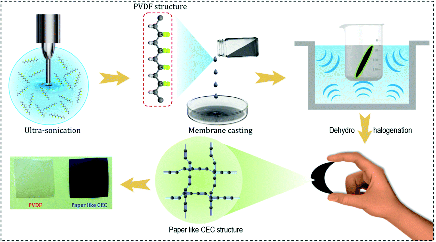
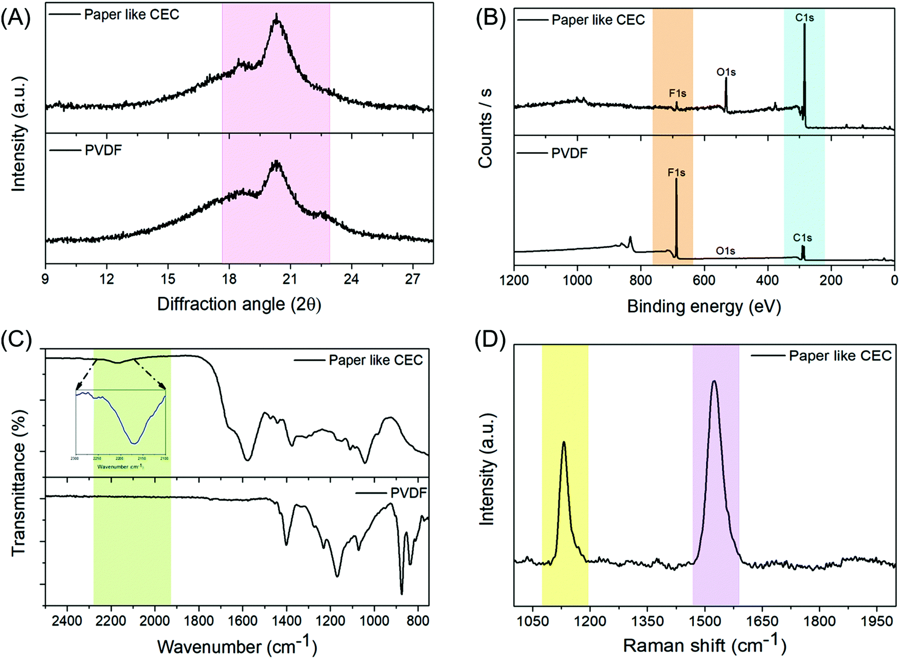
Fig. 1 presents a schematic illustration for the preparation of the free-standing paper-like carbyne-enriched carbon (P-CEC). Polyvinylidene fluoride (PVDF) is a stand-alone candidate, which has received much attention among the polymers due to its exceptional chemical resistance and high mechanical strength.27 This made it suitable as a starting material for the development of new conductive P-CEC films via a one-step dehydrohalogenation reaction.25 The PVDF film prepared via the solvent-casting method was subjected to the dehydrohalogenation process using potassium ethylate in tetrahydrofuran solution. The transformation of the white film into a metallic black film after the dehydrohalogenation process confirmed the formation of the new conductive P-CEC film, as seen in the digital photograph presented in Fig. 1. Fig. 2 displays the physicochemical characterization of the prepared P-CEC film. The comparative X-ray diffractograms (XRD) of the PVDF and P-CEC films are depicted in Fig. 2(A). The XRD pattern of the PVDF film shows a broad peak at 2θ = 20.3°, which is ascribed to the β-phase (orthorhombic structures), while the minor peak (shoulder) at 2θ = 18.4° corresponds to the monoclinic structure of the α-phase. The P-CEC film obtained from PVDF via the exclusion of halogen exhibited a similar diffraction pattern to that of the PVDF film, suggesting that the removal of the halogen did not affect its crystallinity.16,28 To evaluate the changes in surface elemental composition and valence state of the PVDF film before and after the exclusion of halogen via the dehydrohalogenation reaction, X-ray photoelectron spectroscopy (XPS) was performed. Fig. 2(B) displays the comparative XPS full-scale survey spectra of the PVDF and P-CEC films. The survey spectrum of PVDF reveals the presence of carbon and fluorine components. It was observed that after the exclusion of halogen via the dehydrohalogenation process, the intensity of the fluorine component significantly decreased with an increase in the intensity of the carbon component compared to that of former, which confirms the formation of the P-CEC film.25 The relative C 1s core level spectra of the PVDF and P-CEC films are shown in Fig. S1 (ESI†). The C 1s spectrum of PVDF reveals the presence of C–C and C–F, corresponding to the peaks located at 285.5 and 290.5 eV, respectively.29 After the formation of the P-CEC film via the exclusion of halogen, the C–C peaks slightly shifted and narrowed while the C–F peaks significantly decreased compared to the PVDF film. These results suggest the formation of P-CEC from the PVDF film. Fig. 2(C) shows the change in the Fourier infra-red spectrum (FT-IR) after the exclusion of halogen from PVDF via the dehydrohalogenation process. The vibration bands of PVDF located at 877.3, 839.02, and 1232 cm−1 correspond to the α-, β- and γ-phase, respectively.30 After the exclusion of halogen, significant changes were observed in the P-CEC film as follows: (i) the vibrational bands of PVDF at 1399, 1157, and 1067 cm−1 shifted to a lower wavenumber, which may be due to the exclusion of halogen and (ii) two new band were observed at 1578 and 2166 cm−1 mainly attributed to the carbon–carbon vibrations in the polynne structure.31 This result is in good agreement with the previous report.16 The laser Raman spectroscopy study was carried out to examine the structural and functional changes that occurred after the formation of P-CEC from the PVDF film via the dehydrohalogenation process. Fig. S2 (ESI†) depicts the laser Raman spectrum of the PVDF film, which shows the characteristic bands at 807.9 and 844.8 cm−1, corresponding to the α- and β-phase of the prepared PVDF film, respectively, while the peak at 886.7 cm−1 corresponds to the vibration of the C–F and C–C vibrational bands of the PVDF film.32 After the exclusion of halogen from the PVDF film via the dehydrohalogenation process, the laser Raman spectrum of prepared P-CEC film showed two major peaks at 1133.6 and 1530.5 cm−1, as seen in Fig. 2(D). The band observed at 1133.6 cm−1 is attributed to the presence of beta carbyne, whereas the peak at 1530.5 cm−1 corresponds to the vibration of the carbon networks.16,33
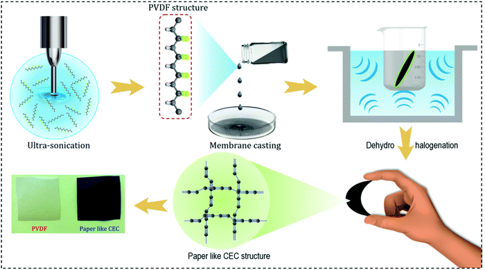 |
| | Fig. 1 Graphical representation of the steps involved in the fabrication of the free-standing paper-like carbyne-enriched carbon film. | |
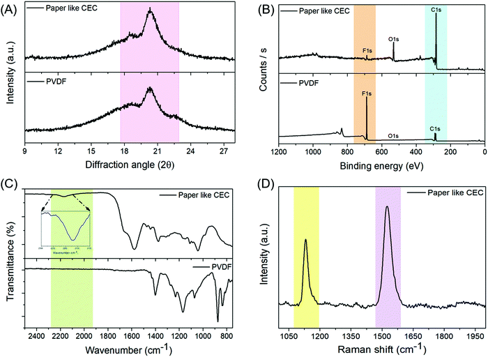 |
| | Fig. 2 Physicochemical characterization of the prepared P-CEC film. (A) Comparative XRD spectra of the PVDF and P-CEC films, (B) relative XPS survey spectra of the PVDF and P-CEC films, (C) comparative FT-IR spectra of the PVDF and P-CEC films, and (D) laser Raman spectrum of the P-CEC film. | |
Fig. 3 depicts the change in surface morphology upon the conversion of the PVDF film to P-CEC. The cross-sectional images of the PVDF and P-CEC films are shown in Fig. 3(A and B), respectively, which revealed that the removal of halogen from PVDF did not affect the thickness of the P-CEC film. The corresponding elemental mapping of the PVDF and P-CEC films is depicted in Fig. S3 and S4 (ESI†), respectively, which further confirms that the dehydrohalogenation process resulted in the removal of halogen (fluorine) from the P-CEC film. Fig. S5(A–C) (ESI†), presents the FE-SEM micrographs of the PVDF film at different magnifications, suggesting its uniform and dense surface with no visible voids on the film. To examine the purity and distribution of the film, the elemental mapping analysis was carried out, as shown in Fig. S5(D) (ESI†). The overlay map reveals the existence of C and F elements in the PVDF film. Moreover, the C and F elements are uniformly distributed throughout the film, as seen in Fig. S5(E and F) (ESI†). The FE-SEM micrograph of the P-CEC film after the removal of halogen is shown in Fig. 3(C). It revealed the presence of voids and uniform surface in the prepared P-CEC film after the dehydrohalogenation reaction, suggesting the removal of halogen from PVDF film. To check the distribution and purity of the prepared P-CEC film, elemental mapping analysis was carried out, as shown in Fig. 3(D–H). The EDS spectrum presented in Fig. 3(D) reveals the ratio of the C, F and O elements present in the prepared P-CEC film. The overlay map of the P-CEC film shows the presence of the C, F, and O elements, as seen in Fig. 3(E), and their corresponding mapping elements are shown in Fig. 3(F–H), respectively, revealing the formation of the P-CEC film. Moreover, the P-CEC film was free-standing with excellent flexibility, which could be bent, twisted and folded freely to form any shape. For example, the digital photograph of the P-CEC film (Fig. 3(I)) shows it could be easily bent (Fig. 3(J)), twisted (Fig. 3(K)) and folded (Fig. 3(L)) according to our requirements. In addition, the elimination of the current collector in the prepared P-CEC film reduced the weight of the device, which significantly increased the energy conversion and storage performances of the device.
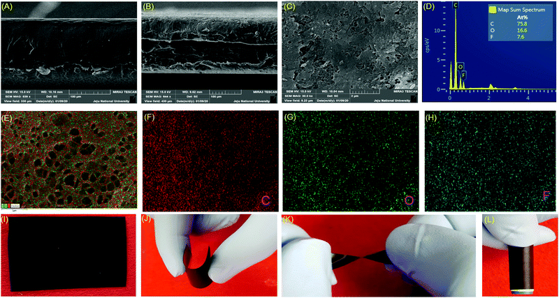 |
| | Fig. 3 FE-SEM analysis of the prepared P-CEC film. (A) Cross-sectional FE-SEM image of PVDF, (B) Cross-sectional FE-SEM micrograph of the P-CEC film after the exclusion of halogen, (C) FE-SEM micrograph of the P-CEC film, (D) EDS spectrum of C, O and F present in the P-CEC film, and (E) overlay map of the P-CEC film obtained using elemental mapping analysis. (F–H) Elemental mapping of C, O and F present in the P-CEC film. (I–L) Pictorial representation of the prepared P-CEC film showing its bending (J), twisting (K) and folding (L) ability. | |
2.2 Energy harvesting properties of P-CEC TENG
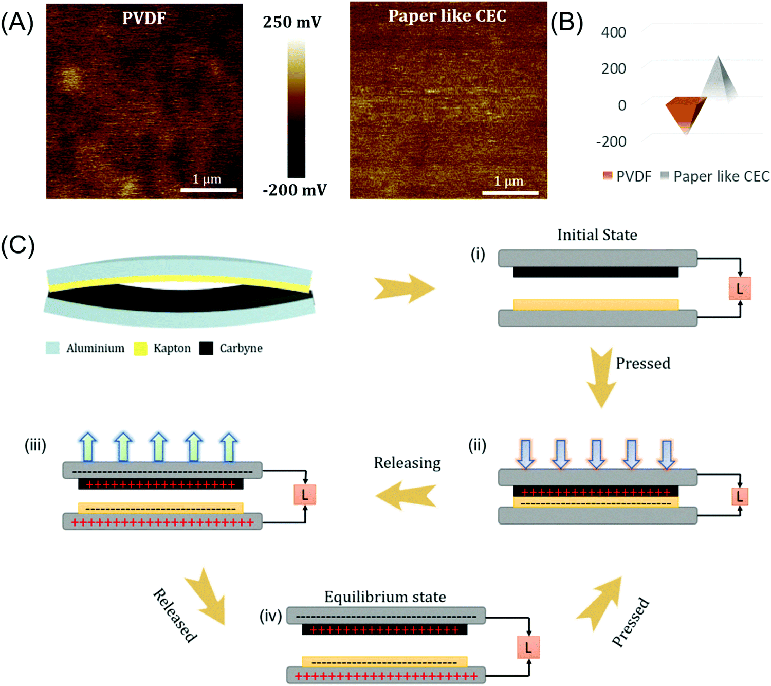
To evaluate the real-time application of the as-prepared P-CEC film, we have examined its use as an active layer in a triboelectric-nanogenerator (TENG) and active electrode material for a symmetric supercapacitor (SSC) considering the state-of-the-art for maintenance-free self-powered system (SPS). Initially, we examined the as-prepared free-standing and flexible P-CEC film directly as a tribo-layer for the fabrication of a TENG. We investigated the surface charge of the obtained film using kelvin probe force microscopy (KPFM) in non-contact mode. Fig. 4(A) and (B) depict the 2D mapping of the surface potential of the PVDF and P-CEC films using Pt tips. Excitingly, after the exclusion of halogen from the PVDF film via the dehydrohalogenation process, the surface charge of the P-CEC film shifts towards a high positive potential (+250 mV) compared to that of the bare PVDF (−200 mV), as evident from Fig. 4(B). The same phenomenon was observed when graphene was added to a pristine PVDF film, confirming that the obtained P-CEC film is an analogue of carbon.34 The positive shift in the surface charge potential of the prepared P-CEC film was anticipated to increase the electrical response of the TENG.35,36 The increase in the surface potential of the P-CEC film (after the exclusion of halogen) was supported by ultra-violet photoelectron spectroscopy (UPS), as depicted in Fig. S6 (ESI†). This shift may be due to the change in the work function of the prepared P-CEC film, which can be determined from the difference between the photon excitation energy and spectrum width.37 From these estimations, the work function of the prepared P-CEC film was found to be 3.37 eV, which is lower compared to that of the pristine PVDF (5.55 eV) and PVDF-G18 (4.84 eV), which is expected to improve the electrical performance of the TENG compared to the bare PVDF film.34 Based on the above result, we constructed a two-arch-based TENG with (i) P-CEC as the positive layer and Kapton as the negative layer and (ii) PVDF as the negative layer and aluminium as the positive layer to evaluate the changes that occurred in the electrical response of the TENG before and after the dehydrohalogenation process. TENG works on the principle of electrostatic induction and contact electrification, and the triboelectric mechanism of the vertical-contact-mode of the P-CEC TENG is depicted in Fig. 4(C). In the initial stage, each layer of P-CEC TENG has no surface charge with zero electric potential, as shown in Fig. 4(C)(i). Once the external compressive force was applied on the P-CEC TENG, the P-CEC and Kapton tribo-layer came into contact with each other, leading to the production of equal and opposite charge on the surface of the P-CEC TENG (as seen in Fig. 4(C)(ii)) due to tribo-electrification. When the external force was removed, the two layers of P-CEC TENG started to be released to their original position slowly, and this separation led to the creation of a potential difference between the layers of the P-CEC TENG. This potential drove the electron flow from the negative layer (Kapton layer) to the positive layer (P-CEC layer) via the external circuit and the maximum electric signal, as shown in Fig. 4(C)(iii). Once the P-CEC TENG was pressed again, electron flow occurred in the opposite direction, which led to the formation of an AC signal, as seen in Fig. 4(C)(iv). When the two layers of P-CEC TENG came into contact, then all the surface charge was neutralized, which resulted in no output.38,39
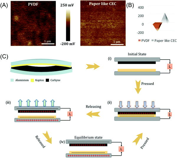 |
| | Fig. 4 (A) Surface potential mapping of the PVDF and P-CEC films analyzed via KPFM measurement, (B) plot of the change in surface potential before and after the exclusion of halogen, and (C) working mechanism of the P-CEC TENG in the vertical contact-separation mode. | |
Fig. 5 depicts the electrical response of the P-CEC TENG. Fig. 5(A) and Fig. S7 (ESI†) show the comparative electrical output voltage and current profile of the PVDF-based TENG and P-CEC TENG measured at the constant force of 10 N. The P-CEC TENG showed a higher output performance (∼117 V and ∼1.2 μA) compared to the PVDF-based TENG (∼14.6 V and ∼220 nA), which may be due to the following reasons: (i) the high surface potential of the P-CEC film compared to the bare PVDF film, (ii) increase in the electrical conductivity of the P-CEC film and (iii) roughness created in the P-CEC film upon the exclusion of halogen via the dehydrohalogenation process compared to that of the PVDF film.40,41 It is well known that surface roughness plays a vital role in the electrical performance of TENGs, and thus we checked the roughness of the PVDF and prepared P-CEC film via AFM analysis, as shown in Fig. S8 (ESI†). As expected, the P-CEC film exhibited a higher roughness than the bare PVDF film, which may be one of the reasons for the high electrical performances of the P-CEC TENG. Fig. 5(B and C) present the voltage and current profiles of the P-CEC TENG obtained at different levels of applied force ranging from 2 N to 15 N, respectively. It is noteworthy that the obtained voltage and current of P-CEC TENG (∼126 V and ∼1.4 μA) was quite higher compared to that of CNT/PDMS TENG (∼40 V and ∼0.8 μA), MoS2/nylon TENG (∼13 V), MoSe2/nylon (∼5.5 V), Graphene/PET (5 V), graphene/PDMS (22 V), and other.42–44Fig. 5(D) and Fig. S10 (ESI†) shows the rectified voltage of the P-CEC TENG at various applied forces. The results shows that the P-CEC TENG delivered the maximum rectified voltage of ∼58 V at an applied compressive force of 15 N. The power and voltage plots of the P-CEC TENG as a function of load resistance are depicted in Fig. 5(E). The maximum power of the P-CEC TENG was ∼27.5 μW (9.28 μW cm−2) at the load resistance of 0.5 GΩ, which is higher compared to that of a polymer-based TENG, carbon-based TENG, and recent 2D material-based TENG.42,45Fig. 5(F) shows the cyclic test of P-CEC TENG over 1500 s, which showed excellent stability without any decay in electrical output over time.
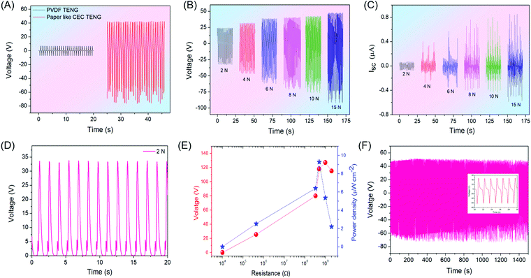 |
| | Fig. 5 (A) Relative output voltage of the PVDF and P-CEC-based TENG, (B and C) output voltage and current of the P-CEC TENG as a function of applied compressive force, respectively, (D) rectified voltage of the P-CEC TENG at a constant applied compressive force of 2 N, (E) output voltage and maximum peak power of the P-CEC TENG as a function of load resistance, and (F) endurance test of the P-CEC TENG over 1500 s at a constant applied force. | |
2.3 Electrochemical performance of P-CEC symmetric supercapacitor
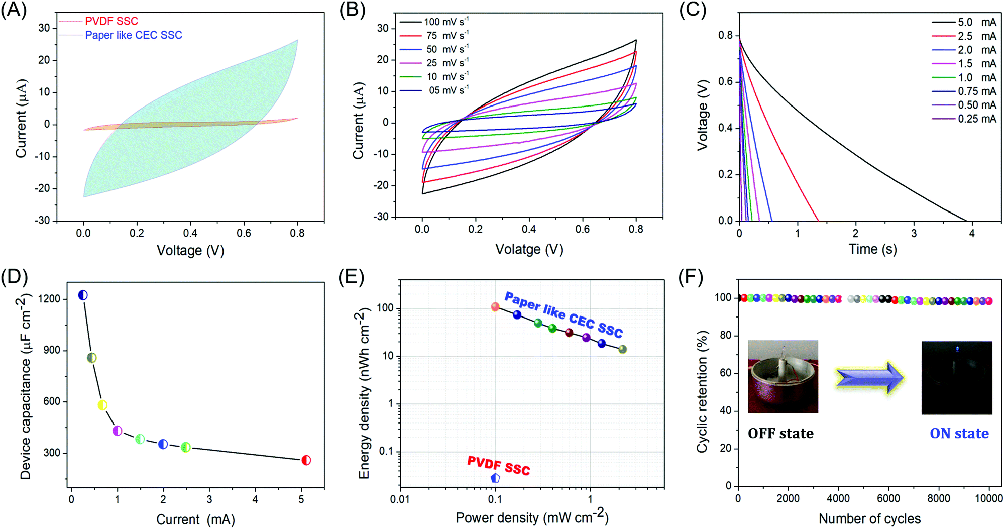
The P-CEC film displayed unique micro-pore/meso-pore structures, high conductivity, and excellent flexibility, which can satisfy the critical requirements of flexible supercapacitors.46,47 Therefore, we also investigated the electrochemical performance of the P-CEC film as a binder-free electrode in the fabrication of a symmetric supercapacitor (SSC) using PVA-Na2SO4 gel electrolyte as the separator.48 The comparative cyclic voltammetry (CV) profiles of PVDF and P-CEC SSC in the voltage window of 0.0 to 0.8 V were recorded at a scan rate of 100 mV s−1, as depicted in Fig. 6(A). As expected, the P-CEC SSC showed better capacitance behaviour compared to the PVDF SSC, which may be due to the unique pore structures and high conductivity of the film. Fig. 6(B) shows the CV profile of the P-CEC film at various scan rates (5 to 100 mV s−1), which suggests ideal rectangular behaviour without any change in its curve, indicating the type A capacitive charge storage mechanism.49Fig. 6(C) portrays the galvanostatic discharge (GD) profile of the P-CEC SSC measured over the voltage window of 0.8 V at different currents ranging from 0.25 to 5 mA, revealing isosceles triangular behaviour, which is consistent with the CV profile (as seen in Fig. 6(B)). The plot of specific capacitance as a function of discharge current is shown in Fig. 6(D). The specific capacitance of the P-CEC film increased with a decrease in discharge current, which may be due to the time constraint of electrolyte ions on the P-CEC film. The maximum specific capacitance of the P-CEC SSC delivered about 1200 μF cm−2 at the current of 0.25 mA. The obtained specific capacitance further confirms the electrochemical behaviour of the P-CEC film since it is known that PVDF is a good insulator and it does not possess electrochemical behaviour. To further analyse the capacitance and resistive behaviour of the P-CEC SSC device, we carried electrochemical impedance spectroscopy (EIS). Fig. S11(A) (ESI†) depicts the Nyquist plot of the P-CEC SSC, which consists of an inobtrusive arc (high frequency) and straight Warburg line (low-frequency region), suggesting ideal capacitive behaviour. The equivalent series resistance (ESR) of the PVDF SSC and P-CEC SSC was found to be 788.8 Ω (Fig. S12, ESI†) and 7.5 Ω, respectively, suggesting the good electrical conductivity of P-CEC SSC after the exclusion of halogen via the dehydrohalogenation process. Fig. S11(B) (ESI†) depicts the Bode phase angle plot of the P-CEC SSC device, indicating a phase angle of about −78.9°, which reveals ideal capacitive behaviour similar to that of other carbon supercapacitors. The Ragone chart is depicted in Fig. 6(E) to estimate the overall performance of the flexible solid-state P-CEC SSC. The energy density of the P-CEC SSC reached up to 109 nW h cm−2 at the low current of 0.25 mA with the maximal power density of 2200 μW cm−2 at the current of 5 mA. Fig. 6(F) displays the endurance test of the P-CEC SSC device over 10![[thin space (1/6-em)]](https://www.rsc.org/images/entities/char_2009.gif) 000 cycles using continuous CD measurement at a current of 1 mA. About 98.3% of its initial capacitance was retained even after 10000 continuous cycles, suggesting the excellent stability of the device. Fig. S13 (ESI†) shows the CV profile of two P-CEC SSC devices connected in series to generate the operating voltage of 1.6 V, suggesting the excellent uniformity of their electrochemical performances. As a proof of concept, the P-CEC SSC devices connected in series were employed to power a blue light-emitting diode, as shown in the inset of Fig. 6(F).
000 cycles using continuous CD measurement at a current of 1 mA. About 98.3% of its initial capacitance was retained even after 10000 continuous cycles, suggesting the excellent stability of the device. Fig. S13 (ESI†) shows the CV profile of two P-CEC SSC devices connected in series to generate the operating voltage of 1.6 V, suggesting the excellent uniformity of their electrochemical performances. As a proof of concept, the P-CEC SSC devices connected in series were employed to power a blue light-emitting diode, as shown in the inset of Fig. 6(F).
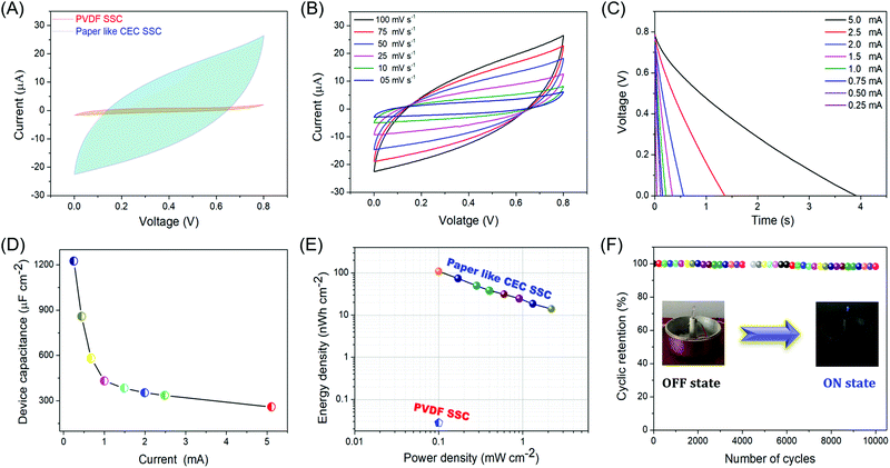 |
| | Fig. 6 Electrochemical performance of the P-CEC SSC device. (A) Relative CV profiles of the PVDF SSC and P-CEC SSC devices tested over the scan rate of 100 mV s−1, (B) CV profile of the P-CEC SSC device at different scan rates (5 to 100 mV s−1), (C) discharge profile of the P-CEC SSC device at various currents in the range of 0.25 to 5.0 mA, (D) variation in the capacitance of the P-CEC SSC device at different currents, (E) ragone chart of the P-CEC SSC device, and (F) cycling performance of the P-CEC SSC device over 10000 cycles at a constant current of 1 mA. | |
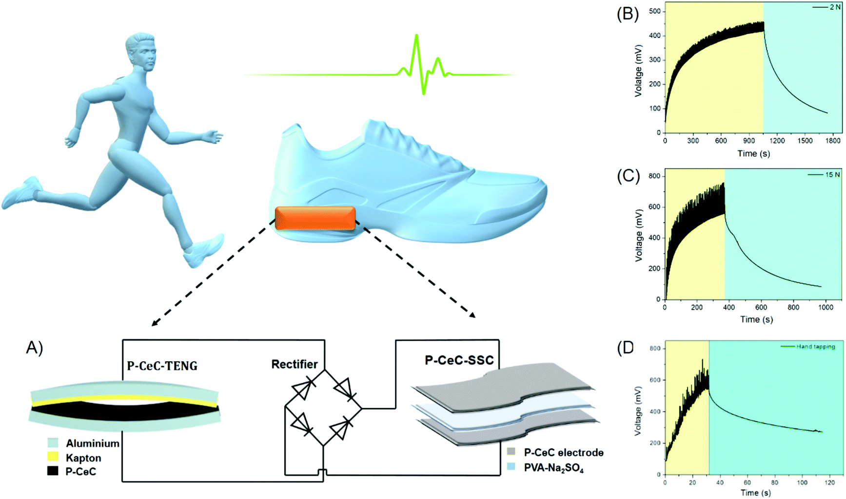
2.4 P-CEC-based self-powered system
Fig. 7 illustrates the maintenance-free self-powered system using the P-CEC film as both the energy harvester and storage unit. The electric circuit of P-CEC-based SPS is shown in Fig. 7(A). Initially, the ability of the PVDF and P-CEC based TENG device to charge a commercial capacitor (1 μF) at the constant applied force of 10 N was tested, as seen in Fig. S14 (ESI†). It revealed that the P-CEC TENG could charge up to 1.75 V within 32 s, while the PVDF TENG charged only 0.6 mV (50 s), suggesting the extraordinary performance of the former compared to the latter. We charged the P-CEC SSC with the P-CEC TENG in vertical contact mode at different force of 2 N (Fig. 7(B)), 8 N (Fig. S15, ESI†) and 15 N (Fig. 7(C)). The P-CEC SSC self-charged to about 750 mV within 380 s under the constant applied force of 15 N and self-discharged to around 600 mV in 620 s, which is high compared to other state-of-the-art SPSs, as evident from Table S1 (ESI†). To demonstrate this, a single P-CEC TENG and P-CEC SSC were connected with a bridge rectifier and attached under a human shoe to check the self-powered system under human motions. This P-CEC SPS self-charged up to 680 mV in 32 s and self-discharged to around 400 mV in 89 s, as seen in Fig. 7(D). All these results show that the P-CEC film will be an effective self-powered system (power source) for the development of next-generation wearable and portable electronic gadgets.
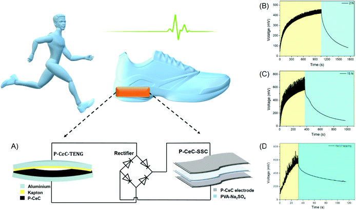 |
| | Fig. 7 Application of P-CEC SPS. (A) Schematic representation of the SPS, (B and C) self-charging properties of the P-CEC SPS under various mechanical force (2 N and 15 N), respectively, and (D) self-charging properties of the P-CEC SPS upon hand flapping. | |
3. Conclusion
In this study, we successfully demonstrated a maintenance-free system using the bifunctional property of a free-standing paper-like carbyne-enriched carbon film (obtained from a thermoplastic polymer) as both a triboelectric nanogenerator and supercapacitor for the first time. The exclusion of halogen from PVDF and formation of the P-CEC film were systematically characterized via XRD, laser Raman spectroscopy, XPS, and FE-SEM analysis. The change in the work function and surface potential of the P-CEC film was methodically analyzed via KPFM and UPS measurement, and the P-CEC TENG delivered the electrical output of ∼126 V and ∼1.4 μA with outstanding stability. The electrochemical properties of P-CEC SSC were superior to that of the PVDF SSC. Furthermore, the SPS (integrated P-CEC TENG and P-CEC SSC) unit showed a superior charge storage property (750 mV within 380 s) compared to state-of-the-art self-powered systems. Herein, we successfully demonstrated the bi-functional properties of a free-standing P-CEC film as a self-powered system, which can be implemented as a polymer-based electrode in advanced maintenance-free systems.
Conflicts of interest
There are no conflicts to declare.
Acknowledgements
This research was supported by the Basic Science Research Program through the National Research Foundation of Korea (NRF) grant funded by the Korea government (MSIT) (2018R1A4A1025998, 2019R1A2C3009747 & 2020R1A2C2007366).
References
- K. Krishnamoorthy, P. Pazhamalai, V. K. Mariappan, S. S. Nardekar, S. Sahoo and S.-J. Kim, Nat. Commun., 2020, 11, 2351 CrossRef CAS PubMed.
- H. Guo, M. H. Yeh, Y. C. Lai, Y. Zi, C. Wu, Z. Wen, C. Hu and Z. L. Wang, ACS Nano, 2016, 10, 10580–10588 CrossRef CAS PubMed.
- J. Wang, X. Li, Y. Zi, S. Wang, Z. Li, L. Zheng, F. Yi, S. Li and Z. L. Wang, Adv. Mater., 2015, 27, 4830–4836 CrossRef CAS PubMed.
- J. Chen, H. Guo, X. Pu, X. Wang, Y. Xi and C. Hu, Nano Energy, 2018, 50, 536–543 CrossRef CAS.
- M. Wakihara, Mater. Sci. Eng., R, 2001, 33, 109–134 CrossRef.
- A. Fotouhi, D. J. Auger, L. O’Neill, T. Cleaver and S. Walus, Energies, 2017, 10(12), 1937 CrossRef.
- S. Sahoo, K. Krishnamoorthy, P. Pazhamalai, V. K. Mariappan, S. Manoharan and S.-J. Kim, J. Mater. Chem. A, 2019, 7, 21693–21703 RSC.
- Z. Chai, N. Zhang, P. Sun, Y. Huang, C. Zhao, H. J. Fan, X. Fan and W. Mai, ACS Nano, 2016, 10, 9201–9207 CrossRef CAS PubMed.
- L. Gao, X. Chen, S. Lu, H. Zhou, W. Xie, J. Chen, M. Qi, H. Yu, X. Mu, Z. L. Wang and Y. Yang, Adv. Energy Mater., 2019, 9, 1902725 CrossRef CAS.
- J. Zhao, H. Li, C. Li, Q. Zhang, J. Sun, X. Wang, J. Guo, L. Xie, J. Xie, B. He, Z. Zhou, C. Lu, W. Lu, G. Zhu and Y. Yao, Nano Energy, 2018, 45, 420–431 CrossRef CAS.
- Q. Zhang, Q. Liang, Q. Liao, M. Ma, F. Gao, X. Zhao, Y. Song, L. Song, X. Xun and Y. Zhang, Adv. Funct. Mater., 2018, 28, 1803117 CrossRef.
- Z. Cong, W. Guo, Z. Guo, Y. Chen, M. Liu, T. Hou, X. Pu, W. Hu and Z. L. Wang, ACS Nano, 2020, 14, 5590–5599 CrossRef CAS PubMed.
- K. Zhao, Q. Qin, H. Wang, Y. Yang, J. Yan and X. Jiang, Nano Energy, 2017, 36, 30–37 CrossRef CAS.
- L. Manjakkal, C. G. Núñez, W. Dang and R. Dahiya, Nano Energy, 2018, 51, 604–612 CrossRef CAS.
- K. Dong, Y. C. Wang, J. Deng, Y. Dai, S. L. Zhang, H. Zou, B. Gu, B. Sun and Z. L. Wang, ACS Nano, 2017, 11, 9490–9499 CrossRef CAS PubMed.
- K. Krishnamoorthy, V. K. Mariappan, P. Pazhamalai, S. Sahoo and S.-J. Kim, Nano Energy, 2019, 59, 453–463 CrossRef CAS.
- L. Shi, S. Dong, P. Ding, J. Chen, S. Liu, S. Huang, H. Xu, U. Farooq, S. Zhang, S. Li and J. Luo, Nano Energy, 2019, 55, 548–557 CrossRef CAS.
- H. Wang, M. Shi, K. Zhu, Z. Su, X. Cheng, Y. Song, X. Chen, Z. Liao, M. Zhang and H. Zhang, Nanoscale, 2016, 8, 18489–18494 RSC.
- K. Poonam, A. A. Sharma and S. K. Tripathi, J. Energy Storage, 2019, 21, 801–825 CrossRef.
- E. H. Falcao and F. Wudl, J. Chem. Technol. Biotechnol., 2007, 82, 524–531 CrossRef CAS.
- Q. Fan, D. Martin-Jimenez, D. Ebeling, C. K. Krug, L. Brechmann, C. Kohlmeyer, G. Hilt, W. Hieringer, A. Schirmeisen and J. M. Gottfried, J. Am. Chem. Soc., 2019, 141, 17713–17720 CrossRef CAS PubMed.
-
Carbyne and Carbynoid Structures, ed. R. B. Heimann, S. E. Evsyukov and L. Kavan, Springer, Netherlands, Dordrecht, 1999, vol. 21 Search PubMed.
- R. Hayatsu, R. G. Scott, M. H. Studier, R. S. Lewis and E. Anders, Science, 1980, 209, 1515–1518 CrossRef CAS PubMed.
- V. I. Artyukhov, M. Liu and B. I. Yakobson, Nano Lett., 2014, 14, 4224–4229 CrossRef CAS PubMed.
- Y. P. Kudryavtsev, S. E. Evsyukov, V. G. Babaev, M. B. Guseva, V. V. Khvostov and L. M. Krechko, Carbon N. Y., 1992, 30, 213–221 CrossRef CAS.
- Y. Liu, W. Wang, A. Wang, Z. Jin, H. Zhao and Y. Yang, Electrochim. Acta, 2017, 232, 142–149 CrossRef CAS.
- G. Dong Kang and Y. Ming Cao, J. Membr. Sci., 2014, 463, 145–165 CrossRef.
- J. A. Januszewski and R. R. Tykwinski, Chem. Soc. Rev., 2014, 43, 3184–3203 RSC.
-
L. M. Blinov, V. M. Fridkin and S. P. Palto.
- X. Cai, T. Lei, D. Sun and L. Lin, RSC Adv., 2017, 7, 15382–15389 RSC.
- F. Cataldo, Polym. Int., 1999, 48, 15–22 CrossRef CAS.
- R. Kumaran, M. Alagar, S. Dinesh Kumar, V. Subramanian and K. Dinakaran, Appl. Phys. Lett., 2015, 107, 113107 CrossRef.
- N. N. Mel’nik, D. Y. Korobov, O. S. Plyashechnik and V. V. Savranskii, Bull. Lebedev Phys. Inst., 2013, 40, 187–190 CrossRef.
- J. W. Lee, H. J. Cho, J. Chun, K. N. Kim, S. Kim, C. W. Ahn, I. W. Kim, J. Y. Kim, S. W. Kim, C. Yang and J. M. Baik, Sci. Adv., 2017, 3(5), e1602902 CrossRef PubMed.
- Z. L. Wang, J. Chen and L. Lin, Energy Environ. Sci., 2015, 8, 2250–2282 RSC.
- H. Oh, S. S. Kwak, B. Kim, E. Han, G. H. Lim, S. W. Kim and B. Lim, Adv. Funct. Mater., 2019, 29, 1–6 Search PubMed.
- S. A. Pawar, D. Kim, A. Kim, J. H. Park, J. C. Shin, T. W. Kim and H. J. Kim, Opt. Mater., 2018, 86, 576–581 CrossRef CAS.
- Y. Wang, Y. Yang and Z. L. Wang, npj Flexible Electron., 2017, 1, 10 CrossRef.
- Z. L. Wang, ACS Nano, 2013, 7, 9533–9557 CrossRef CAS PubMed.
- J. Chun, B. U. Ye, J. W. Lee, D. Choi, C. Y. Kang, S. W. Kim, Z. L. Wang and J. M. Baik, Nat. Commun., 2016, 7, 1–9 Search PubMed.
- J. Chen, H. Guo, X. He, G. Liu, Y. Xi, H. Shi and C. Hu, ACS Appl. Mater. Interfaces, 2016, 8, 736–744 CrossRef CAS PubMed.
- M. Seol, S. Kim, Y. Cho, K.-E. Byun, H. Kim, J. Kim, S. K. Kim, S.-W. Kim, H.-J. Shin and S. Park, Adv. Mater., 2018, 30, 1801210 CrossRef PubMed.
- S. Kim, M. K. Gupta, K. Y. Lee, A. Sohn, T. Y. Kim, K.-S. Shin, D. Kim, S. K. Kim, K. H. Lee, H.-J. Shin, D.-W. Kim and S.-W. Kim, Adv. Mater., 2014, 26, 3918–3925 CrossRef CAS PubMed.
- B. N. Chandrashekar, B. Deng, A. S. Smitha, Y. Chen, C. Tan, H. Zhang, H. Peng and Z. Liu, Adv. Mater., 2015, 27, 5210–5216 CrossRef CAS PubMed.
- S. A. Han, J. Lee, J. Lin, S.-W. Kim and J. H. Kim, Nano Energy, 2019, 57, 680–691 CrossRef CAS.
- D. W. Kim, S. M. Jung and H. Y. Jung, J. Mater. Chem. A, 2020, 8, 532–542 RSC.
- V. K. Mariappan, K. Krishnamoorthy, P. Pazhamalai, S. Sahoo, S. S. Nardekar and S.-J. Kim, Nano Energy, 2019, 57, 307–316 CrossRef CAS.
- K. Krishnamoorthy, P. Pazhamalai and S.-J. Kim, Energy Environ. Sci., 2018, 11, 1595–1602 RSC.
- Y. Gogotsi and R. M. Penner, ACS Nano, 2018, 12, 2081–2083 CrossRef CAS PubMed.
Footnote |
| † Electronic supplementary information (ESI) available. See DOI: 10.1039/d0ma00324g |
|
| This journal is © The Royal Society of Chemistry 2020 |
Click here to see how this site uses Cookies. View our privacy policy here. 
 Open Access Article
 This Open Access Article is licensed under a Creative Commons Attribution-Non Commercial 3.0 Unported Licence
 a,
Karthikeyan
Krishnamoorthy
a,
Karthikeyan
Krishnamoorthy